Enhanced photoresponse of a metal-oxide-semiconductor photodetector with silicon
nanocrystals embedded in the oxide layer
Jia-Min Shieh, Yi-Fan Lai, Wei-Xin Ni, Hao-Chung Kuo, Chih-Yao Fang, Jung Y. Huang, and Ci-Ling Pan
Citation: Applied Physics Letters 90, 051105 (2007); doi: 10.1063/1.2450653
View online: http://dx.doi.org/10.1063/1.2450653
View Table of Contents: http://scitation.aip.org/content/aip/journal/apl/90/5?ver=pdfcov Published by the AIP Publishing
Articles you may be interested in
Effects of postgate dielectric treatment on germanium-based metal-oxide-semiconductor device by supercritical fluid technology
Appl. Phys. Lett. 96, 112902 (2010); 10.1063/1.3365177
Near-infrared silicon quantum dots metal-oxide-semiconductor field-effect transistor photodetector Appl. Phys. Lett. 94, 241108 (2009); 10.1063/1.3156806
Superlinear photovoltaic effect in Si nanocrystals based metal-insulator-semiconductor devices Appl. Phys. Lett. 94, 062108 (2009); 10.1063/1.3081410
Subband gap photoresponse of nanocrystalline silicon in a metal-oxide-semiconductor device J. Appl. Phys. 104, 074917 (2008); 10.1063/1.2999561
Si avalanche photodetectors fabricated in standard complementary metal-oxide-semiconductor process Appl. Phys. Lett. 90, 151118 (2007); 10.1063/1.2722028
This article is copyrighted as indicated in the article. Reuse of AIP content is subject to the terms at: http://scitation.aip.org/termsconditions. Downloaded to IP: 140.113.38.11 On: Thu, 01 May 2014 00:41:13
Enhanced photoresponse of a metal-oxide-semiconductor photodetector
with silicon nanocrystals embedded in the oxide layer
Jia-Min Shieh,a兲Yi-Fan Lai, and Wei-Xin Ni
National Nano Device Laboratories, No. 26 Prosperity Road 1, Hsinchu, Taiwan 30078, Republic of China
Hao-Chung Kuo, Chih-Yao Fang, Jung Y. Huang, and Ci-Ling Pan
Department of Photonics and Institute of Electro-Optical Engineering, National Chiao Tung University, 1001 Ta Hsueh Road, Hsinchu, Taiwan 30010, Republic of China
共Received 24 October 2006; accepted 6 January 2007; published online 30 January 2007兲 The authors report a two-terminal metal-oxide-semiconductor photodetector for which light is absorbed in a capping layer of silicon nanocrystals embedded in a mesoporous silica matrix on
p-type silicon substrates. Operated at reverse bias, enhanced photoresponse from 300 to 700 nm
was observed. The highest optoelectronic conversion efficiency is as high as 200%. The enhancements were explained by a transistorlike mechanism, in which the inversion layer acts as the emitter and trapped positive charges in the mesoporous dielectric layer assist carrier injection from the inversion layer to the contact, such that the primary photocurrent could be amplified. © 2007 American Institute of Physics.关DOI:10.1063/1.2450653兴
Photodetectors are essential optoelectronic devices1for a variety of applications, ranging from biomedicine2to optical storage.3Although bulk silicon共Si兲 has been widely used in the mainstream electronic chip technology, so far it fails for device applications in optoelectronics due to an indirect band gap of 1.1 eV. Nanoscaled engineered Si materials with size-dependent properties in electronic states,4 however, are po-tential candidates for photonic devices. In particular, two kinds of Si-based nanostructured materials, namely, thin films of silicon nanocrystals5 共nc-Si, 1–2 nm in characteris-tic size兲 and porous silicon,6,7were shown to be efficient for photodetection with spectral response from near infrared to the ultraviolet共UV兲.
Detection amplification in photodetectors is a concern and also gives another means to enhance the device sensitivity,8i.e., although the primary photoresponse may not be very high, the eventually measured photocurrent could be improved due to the device amplification function. The known detector solutions of this type are the avalanche photodiodes,9 phototransistors,10 photo-metal-oxide-semiconductor field-effect transistors,11etc.
In this letter, we report enhanced spectral photoresponse from a two-terminal metal-oxide-semiconductor共MOS兲-type detector with a capping layer of nc-Si-embedded mesoporous silica12 共MS兲 and the enhancement is attributed to the tran-sistorlike operation of the device, in which the inversion layer acts as the emitter while trapping of positive charges in the mesoporous dielectric layer assists the carrier injection from the inversion layer to the contact, resulting in current amplification.
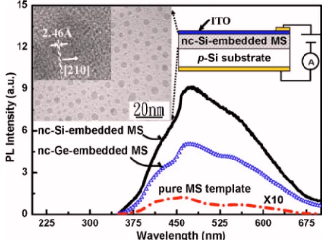
The device structure is depicted schematically in Fig.1. First, a 220-nm-thick MS template layer is formed on p-type Si substrates. Si nanocrystals were thereafter synthesized in the MS templates by using a plasma deposition process.12 The size and crystalline nature of these embedded Si nano-crystals are revealed in the inset of Fig. 1 by a high-resolution image of cross-sectional transmission electron mi-croscopy 共TEM兲. One can see that the density of Si
nanocrystals in the MS film was in the order of 2 ⫻1018cm−3. The average size of nc-Si was found to be
⬃4 nm. For applying bias, a back Al contact layer and a top 共transparent兲 indium tin oxide 共ITO兲 electrode of 2 ⫻2.5 mm2are formed.
The photoluminescence 共PL兲 spectra of the nanostruc-tured films shown in Fig. 1 exhibit a broadband peak at 2.7 eV共=460 nm兲. Similar PL spectra were also observed from the germanium nanocrystals 共nc-Ge兲-embedded samples, as well as the reference sample of a pure MS template12 but with a much lower intensity, indicating that the emission was weakly linked to the embedded nanocrystal structures. Hence, we attribute the observed blue PL emis-sion to the interfacial states associated with neutral defects of oxygen vacancy13 共wSi–Siw兲 in the MS matrix. The em-bedded semiconductor nanocrystals, e.g., nc-Si, in the silica layer play a role by sensitizing the emission through gener-ating more photoexcited carriers. These carriers are then trapped in the interfacial oxygen defects and subsequently
a兲Electronic mail: [email protected]
FIG. 1. 共Color online兲 PL spectra of MS films embedded with Si or Ge nanocrystals, as well as the pure MS template, together with a schematic drawing illustrating the configuration of the ITO/nc-Si-embedded MS/ p-Si photodetectors. The inset shows cross-sectional TEM images of the MS films with high density of silicon nanocrystals.
APPLIED PHYSICS LETTERS 90, 051105共2007兲
0003-6951/2007/90共5兲/051105/3/$23.00 90, 051105-1 © 2007 American Institute of Physics
This article is copyrighted as indicated in the article. Reuse of AIP content is subject to the terms at: http://scitation.aip.org/termsconditions. Downloaded to IP: 140.113.38.11 On: Thu, 01 May 2014 00:41:13
recombine for an intense 460 nm PL emission. A shoulder peak also appeared in the spectra around 550– 575 nm, which could be due to the band-to-band transition of Si nanocrystals with double-bonded oxygen atoms.14
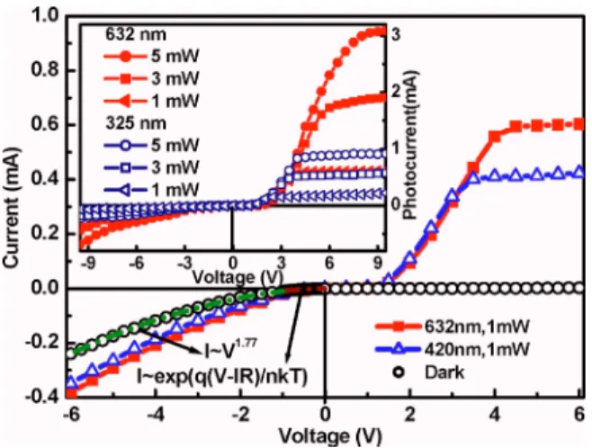
Figure 2 shows current-voltage 共I-V兲 characteristics of the device without illumination. A rectifying ratio of 87 was measured at ±3 V. In the range of low forward bias from 0 to − 0.9 V, the I-V characteristic was fitted fairly using the equation given in Ref.15 and presented in Fig.2 by series connection of a diode 共ideality factor ⬇2.1兲 and a resistor 共75 k⍀兲. Over this range, a bias dependence of ⬃V1.77 was
obtained, indicating that space-charge-limited current domi-nates I-V characteristics.16 Weak photoresponse was ob-served over a wide range of forward bias voltages 共0 to − 6 V兲 when the device was irradiated with 420 and 632 nm light of 1 mW, respectively共Fig.2兲.
Very different I-V characteristics were observed at re-verse bias. As shown in Fig. 2, for the bias ⬎1.5 V the originally very low reverse current共hereafter referred to as the dark current兲 increased drastically when the device was illuminated with light in the wavelength range of 300– 700 nm共only several typical curves are depicted here兲. The increase of photocurrent exhibited a linear dependence with increase of voltage at lower reverse bias until the cur-rent saturated to a value IS at higher bias. Note that IS
in-creases with the incident light power at a given wavelength, while it is higher for incident light of the same power but at longer wavelengths共see the inset of Fig.2兲.
Figure3summarizes the measured photoresponse over a wide range of incident light wavelengths for the ITO/nc-Si-embedded MS/ p-Si MOS detectors at bias voltages of ±5 V, together with a reference curve obtained for the same device structure but without a capping layer, namely, ITO/ p-Si di-odes. The photoresponse values plotted in the figure were calculated after subtracting the dark current at the corre-sponding bias. Biased at +5 V, the photoresponse of an ITO/ p-Si structure increased essentially linearly with wave-length from 300 to 700 nm by three times. The ITO/nc-Si-embedded MS/ p-Si detector showed essentially the same spectral response for both forward and reverse biases, except for the two peaks observed at 425 and 580 nm. Significantly,
much more enhanced photoresponse 共a factor of 4–5兲 was measured at reverse bias, which were as high as 0.4 and 0.9 A / W at the above two wavelengths, respectively.
For convenience, two guidelines were plotted in Fig. 3, representing the quantum efficiency共兲 values of 100% and 200%, respectively. For two spectral ranges, i.e., 375–475 and 500– 650 nm, we measured conversion efficiency values of more than 100% and as high as nearly 200% at 580 nm for the ITO/nc-Si-embedded MS/ p-Si detector. Therefore, there must be an amplification mechanism to enhance the measured photoresponse at reverse bias. Furthermore, it is noted that the enhancement factor between forward and re-verse cases is independent of illumination intensity if dark current is subtracted共see the inset of Fig.2兲. Low dark
cur-rents with high dynamic resistance of 1.3 M⍀ and high pho-toresponse yield high detectivity of ⬃共1–2兲 ⫻1012cm Hz0.5W−1 for the present detector.17
The measured response time of the detector was around 10 ns presumably constrained by nonradiative lifetime 共2.5 ns兲 as previously reported in mesoporous siliceous materials.18 This value is much faster than those demon-strated by photoconductive detectors.5,8 Hence, photocon-ductive gain was ruled out as a major mechanism in the enhancement of reverse photocurrents of our ITO/nc-Si-embedded MS/ p-Si detectors.5,8,19
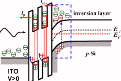
Based on the above experimental evidence, we propose the following mechanism to explain why the detector effi-ciency could be more than 100% through this two-terminal detector with a nc-Si-embedded MS layer as the absorption medium. This is illustrated in Fig.4. Before illumination, the device operates like a normal MOS capacitor, i.e., a signifi-cant number of electrons are accumulated at the MS-Si in-terface forming a n-type inversion layer if a large enough reverse bias is applied. Only a few carriers could flow over the MS barrier layer, leading to a considerably low dark cur-rent. Upon optical excitation, strong absorption occurs for incident photons with the energies matching the transition energies from the ground hole states共Eh
0兲 to the ground
elec-tron states共Ee0兲 共the gap energy between the highest occupied
molecular orbital and the lowest unoccupied molecular or-bital according to Ref14兲, and the ground hole states 共Eh
0兲 to
the excited states 共Ee
*兲 in connection to the Si–O interface
states as well. With the applied electric field, the excited electrons in the Ee0and Ee*states are driven towards the ITO contact layer via the tunneling process. The holes, however,
FIG. 2. 共Color online兲 Current-voltage characteristics of ITO/nc-Si-embedded MS/ p-Si devices in the dark and illuminated by 420 and 632 nm light of 1 mW. The inset is a plot of photocurrents for the same device irradiated with 325 and 632 nm light of 1, 3, and 5 mW, respectively, in which the photocurrents mean the measured current values after subtraction of the dark current.
FIG. 3. 共Color online兲 Spectral dependence of the photoresponse of detec-tors with ITO/nc-Si-embedded MS/ p-Si and ITO/ p-Si structures.
051105-2 Shieh et al. Appl. Phys. Lett. 90, 051105共2007兲
This article is copyrighted as indicated in the article. Reuse of AIP content is subject to the terms at: http://scitation.aip.org/termsconditions. Downloaded to IP: 140.113.38.11 On: Thu, 01 May 2014 00:41:13
will be trapped by the interface states20with the energy level somewhat above the ground hole state共Eh
0兲. The immobile
positive charge centers will subsequently lower the barrier height, causing the resonant injection of electrons from the inversion layer through the MS layer to the ITO contact. Therefore, the measured photocurrent is expected to be com-posed of two parts, i.e., the photoexcited electrons plus the injected electrons. The mechanism of current amplification observed in this work is thus similar to that of a conventional phototransistor.10 In particular, the enhancement of photore-sponsivity measured at 425 and 580 nm, respectively, can be explained by the two resonant states of the nc-Si/MS system.4,14,20
The situation is different when the gate bias is changed from positive to negative. Although excited electrons in this case are expected to move to the side of the Si substrate, recombination with holes in the surface accumulation layer will significantly reduce the charge transport. At the same time, there will be little enhancement of hole transport from the MS layer to ITO, since the photogenerated holes are mostly trapped at the interface states. Therefore, the mea-sured current would not differ too much from the case with-out photoexcitation.
In summary, we demonstrated efficient ITO/nc-Si-embedded MS/ p-Si MOS detectors with enhanced photore-sponse from UV to visible light. The enhancement effect was explained by the transistorlike operation mechanism when the device was operated at reverse bias. The primary
photo-current generated in the nc-Si of the MS layer was amplified due to the electron injection from the inversion layer through the MS dielectric to the ITO contact. Therefore, the mea-sured optoelectronic conversion efficiency can be as high as 200%.
The authors acknowledge the financial support by the National Science Council of Taiwan共NSCT兲 through various grants including PPAEU-II and the ATU program of the Min-istry of Education, Taiwan, R.O.C.
1P. Yu, J. Topolancik, and P. Bhattacharya, IEEE J. Quantum Electron. 40,
1417共2004兲.
2H. Ouyang, C. C. Striemer, and P. M. Fauchet, Appl. Phys. Lett. 88,
163108共2006兲.
3F. Gan, L. Hou, G. Wang, H. Liu, and J. Li, Mater. Sci. Eng., B 76, 63
共2000兲.
4M. V. Wolkin, J. Jorne, P. M. Fauchet, G. Allan, and C. Delerue, Phys.
Rev. Lett. 82, 197共1999兲.
5O. M. Nayfeh, S. Rao, A. Smith, J. Therrien, and M. H. Nayfeh, IEEE
Photonics Technol. Lett. 16, 1927共2004兲.
6J. P. Zheng, K. L. Jiao, W. P. Shen, W. A. Anderson, and H. S. Kwok,
Appl. Phys. Lett. 61, 459共1992兲.
7M. K. Lee, C. H. Chu, Y. H. Wang, and S. M. Sze, Opt. Lett. 26, 160
共2001兲.
8S. M. Sze, Physics of Semiconductor Devices, 2nd ed.共Wiley, New York,
1981兲, Chap. 13, pp. 743–770.
9R. McClintock, A. Yasan, K. Minder, P. Kung, and M. Razeghi, Appl.
Phys. Lett. 87, 241123共2005兲.
10A. Elfving, M. Larsson, G. V. Hansson, P.-O. Holtz, and W.-X. Ni, Mater.
Res. Soc. Symp. Proc. 770, I2.2共2003兲.
11A. Elfving, A. Karim, G. V. Hansson, and W.-X. Ni, Appl. Phys. Lett. 89,
083510共2006兲.
12A. T. Cho, J. M. Shieh, J. Shieh, Y. F. Lai, B. T. Dai, F. M. Pan, H. C. Ku,
Y. C. Lin, K. J. Chao, and P. H. Liu, Electrochem. Solid-State Lett. 8, G143共2005兲.
13J. Y. Zhang, X. M. Bao, Y. H. Ye, and X. L. Tan, Appl. Phys. Lett. 73,
1790共1998兲.
14A. Puzder, A. J. Williamson, J. C. Grossman, and G. Galli, Phys. Rev.
Lett. 88, 097401共2002兲.
15T. A. Burr, A. A. Seraphin, E. Werwa, and K. D. Kolenbrander, Phys. Rev.
B 56, 4818共1997兲.
16M. A. Rafiq, Y. Tsuchiya, H. Mizuta, S. Oda, Shigeyasu Uno, Z. A. K.
Durrani, and W. I. Milne, Appl. Phys. Lett. 87, 182101共2005兲.
17C. K. Wang, T. K. Ko, C. S. Chang, S. J. Chang, Y. K. Su, T. C. Wen, C.
H. Kuo, and Y. Z. Chiou, IEEE Photonics Technol. Lett. 17, 2161共2005兲.
18Y. L. Liu, W. Z. Lee, J. L. Shen, Y. C. Lee, P. W. Cheng, and C. F. Cheng,
Appl. Phys. Lett. 85, 6350共2004兲.
19S. K. Zhang, W. B. Wang, I. Shtau, F. Yun, L. He, H. Morkoc, X. Zhou, M.
Tamargo, and R. R. Alfano, Appl. Phys. Lett. 81, 4862共2002兲.
20S. H. Choi and R. G. Elliman, Appl. Phys. Lett. 74, 3987共1999兲.
FIG. 4.共Color online兲 Illustration of transistorlike operation of an ITO/nc-Si-embedded MS/ p-Si device under reveres bias and illumination. The sym-bols lpand linvin the figure represent photoexcited and injected currents,
respectively.
051105-3 Shieh et al. Appl. Phys. Lett. 90, 051105共2007兲
This article is copyrighted as indicated in the article. Reuse of AIP content is subject to the terms at: http://scitation.aip.org/termsconditions. Downloaded to IP: 140.113.38.11 On: Thu, 01 May 2014 00:41:13