A Fully Integrated Spread Spectrum Clock Generator
Using Two-Point Delta-Sigma Modulation
Yi-Bin Hsieh
Institute of Communication Engineering National Chiao-Tung University,
Hsin-Chu, Taiwan 30050 yibin.cm93g@nctu.edu.tw
Yao-Huang Kao
Department of Communication Engineering Chung-Hua University,
Hsin-Chu, Taiwan 300 yhkao@chu.edu.tw Abstract—A new spread spectrum clock generator (SSCG)
using two-point delta-sigma modulation is presented in this paper. Not only the divider is varied, but also the voltage controlled oscillator is modulated. This technique can enhance the modulation bandwidth so that the effect of EMI suppression is improved. In addition, the method of two-path is applied to the loop filter to reduce the capacitance value such that the total integration can be achieved. The proposed SSG has been fabricated in a 0.35um CMOS process. The clock of 400MHz with center spread ratios of 1.25% and 2.5% are verified. The size of chip area is 0.90×0.89mm2.
I. INTRODUCTION
Spread-spectrum clock generators (SSCG) have been widely employed as high-speed sources with reduced EMI levels [1]-[7]. Basically, SSCG is a phase locked loop (PLL) with special case of frequency modulation. There are two kinds of modulation techniques employed in PLLs. One is to control the variation of the divider and the other is to modulate the VCO directly. In the former case a fractional-N PLL with a ΣΔ modulator is mostly used [1]-[7]. It has the advantage of being fully digital controlled. The modulator is controlled by a triangular wave generator. The loop bandwidth is traded off between modulation profile and jitter caused by ΣΔ modulator. As the loop bandwidth is not wide enough, the modulation profile is distorted and the effect of EMI suppression is reduced. The method of distorted triangle waveform has been presented to improve the modulation profile [8]. Here, the method of two-point modulation is presented to enhance the bandwidth and, in the meantime, maintain the linear saw-tooth waveform.
Actually two-point modulation in PLL has been used in the frequency generator with DC-FM feature. The transfer function appears as all-pass behavior with fine parameter adjustment. Recently, this technique is employed in frequency hopping spread-spectrum systems (FHSS) [9]. In this study, a modified SSCG with two-point modulation with dual-path loop filter (TPDL-SSCG) is presented to achieve wide bandwidth and full integration.
II. PROPOSED TPDL-SSCG
The typical architecture of two-point modulation is shown in Fig. 1. There are two modulation points. One point is at the input of multi-modulus divider through the ΣΔ modulator. The other point is at the input of VCO through a DAC and a reconstruction filter. Usually a high resolution DAC is needed to achieve better performance due to the small modulation amplitude appeared at the input of VCO. It means high power consumption and has large area penalty. To achieve the total integration, the architecture is modified. The block diagram of proposed TPDL-SSCG is shown in Fig. 2 with a PFD, a dual path loop filter, a VCO, a 8-bit programmable counter (PGC), a digital ΣΔ modulator, a modulation profile generator, and a proposed DAC. The dual-path loop filter [10] consists of CP1, CP2, C1, C2, R1, and a unity-gain amplifier. The proposed DAC consists of a digital slicer, CP3, and C1. The modulation profile generator produces a digital triangular wave, Fsig, to feed into the digital ΣΔ modulator and the digital slicer simultaneously. The digital slicer slices the triangular wave into a digital clock. Then, the digital clock charges and discharges the C1 through the CP3 to finish digital to analog conversion. Because the digital slicer, the modulation profile generator
Identify applicable sponsor/s here. (sponsors)
Figure 1. The typical TPDSM architecture [9]
2156
and the digital ΣΔ modulator use the same clock domain, Fbk, the output of digital slicer can be tracked with triangular wave very well and the delay mismatch between two points can be eliminated.
Assume that Ip3 is the current of CP3. Ignoring CP1 and CP2, the relation between VCO controlled voltage Vc and Ip3 is 3 1
1
c pV
I
≈
sC
(1)under the condition of Fsig<<1/(2πR1C2). According to (1), the analog modulation signal (the analog triangular wave) is created as Ip3 is a square wave. Here C1 with one grounded terminal is implemented by the accumulation MOS capacitor to save area and has good distortion performance when the gate-source bias voltage is equal to or large than 1V [13]. The relation between Ip3 and spreading ratio δ% is predicted as 3 1
%
2
p vco m cI K
C f f
δ
=
(2)where fc is nominal output frequency, fm is the modulation frequency of the triangle wave and Kvco is the conversion gain of VCO.
The linear model of TPDL-SSCG is shown in Fig. 3. Φout is the phase of output signal Fout. Φsig is the phase of modulation signal. Gm is the gain factor for compensation between two modulation points. According to (2), the gain mismatch comes from the process variation of Kvco, Ip3, and C1. Here the delay mismatch is assumed to be ignored due to the proposed DAC architecture. Kd is gain of the PFD and charge pump. F(s) is dual-path loop filter transfer function. The divider value is N. Assume that Ip1 is the current of CP1, Ip2 is the current of CP2 and Ip1=BIp2. Here B=4. Ignoring the loading of CP3, we can get the following relationship.
( )
1(
1)
1 1 1 21
1
c pR s
R BC
V
F s
I
s
sR C
⎛
⎞
+
⎜
⎟
⎝
⎠
=
=
+
. (3)From (3), the zero is at 1/(BC1)R1. Obviously, the magnitude of capacitance C1 can be reduced by the factor B. It is a favor for total integration. The closed loop transfer function of Fig. 3 can be derived as
( )
( )
( )
vco d out
m
sig vco d vco d
K K F s
Ns
G
Ns K K F s
Ns K K F s
Φ
=
+
×
Φ
+
+
. (4)The first term in the right hand side appears as a low pass and second term appears as a high pass as F(s) in (3) is taken into account. From (4), Φout is equal to Φsig if Gm=1. It means that if there are no any mismatches between two modulation points, the output signal can be modulated without distortion and bandwidth limitation.
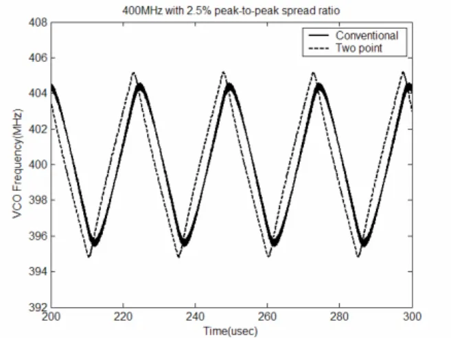
The behavior simulation results by Matlab are shown in Fig. 4. The simulation condition is that the output frequency is 400MHz with the spread ratio of 2.5%, the modulation frequency is 40KHz, and the loop bandwidth is about 70KHz. The solid line represents the traditional SSCG using fractional-N PLL. The dashed line represents the proposed TPDL-SSCG. From the simulation, we can see clearly the advantage of TPDL-SSCG that the distortion is less than the traditional one, and the modulation profile is more like a
Figure 2. The block diagram of TPDL-SSCG
Figure 3. Linear model of TPDL-SSCG
Figure 4. Simulation results of tranditonal SSCG and TPDL-SSCG.
triangular wave even when the loop bandwidth is not wide enough.
III. CIRCUIT DESCRIPTIONS
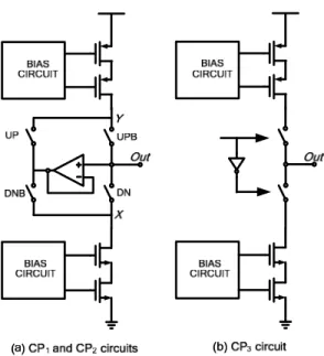
The circuits used in the work are described briefly next. The charge-pump of CP1(2) and CP3 are shown in Fig. 5(a) and 5(b), respectively. The cascoded current sources with wide-swing bias circuit in Fig. 5 are employed for good immunity against the power supply noise. The controlling signals for UP, UPB, DN and DNB switches are fed from the outputs of PFD. The input of CP3 is from the output of digital slicer. A unity-gain buffer for CP1 and CP2 is used to reduce the charge sharing when switching. The unity-gain buffer is not needed for CP3 due to the low input frequency. The low jitter wide band VCO [11] with sharp output waveform and full swing is employed here. The MASH-1-1 ΣΔ modulator with extended input range [7] is used here due to the advantage of unconditional stability, small area and wide input range.
IV. MEASUREMENT RESULTS
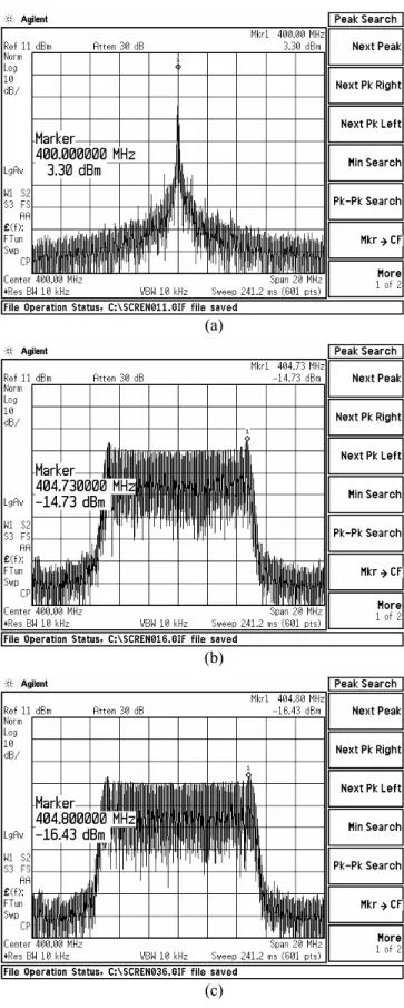
The TPDL-SSCG is designed and fabricated by TSMC 0.35um single-poly quadruple-metal CMOS process. The die photograph is shown in Fig. 6 with area equal to 0.90×0.89 mm2. The output spectrum without spreading is shown in Fig. 7(a) with clock speed at 400MHz. The amplitude of the peak is 3.30dBm. The output spectrum using traditional SSCG with 2.5% spread ratio is shown in Fig. 7(b). The amplitude is reduced to -14.73dBm. The peak reduction is about 18.03dB compared to that in Fig. 7(a). There exist two small peaks at two edges due to insufficient loop bandwidth. The output spectrum using the proposed TPDL-SSCG with the same spread ratio is shown in Fig. 7(c). The amplitude is -16.43dBm. The peak reduction factor is about 19.73dB compared to that in Fig. 7(a). The proposed TPDL-SSCG has
1.70dB improvement in EMI reduction. Table I gives the performance summary of TPDL-SSCG
V. CONCLUSION
In this study, the spread spectrum clock generator with two-point modulation is presented. The modulation bandwidth is effectively expanded with two-point modulation. The modulation profile is improved to be nearly linear. In the meantime the total integration without external loop filter and a high resolution DAC is realized. The improvement of EMI reduction is better than 1.70dB with respect to the conventional one.
ACKNOWLEDGMENT
The authors would like to thank National Chip Implementation Center and National Science Council, Taiwan, R.O.C., for chip implementation and financial support.
TABLE I. PERFORMANCE SUMMARY
Modulation Method Two point
Modulation Type Center-spread
Modulation Frequency 40KHz Spread Ratios(pp) 1.25%, 2.5% Output Frequency 400MHz Input Frequency 14.31818MHz Loop bandwidth ~70KHz Loop filter R1=12KΩ C1=400pF C2=40pF
EMI reduction 19.73dB @ 2.5% center spread ratio
Chip Area (active) 0.90×0.89 mm2
Power Dissipation 33mW including output buffer @ 3.0V Figure 6. Die photograph of the proposed TPDL-SSCG Figure 5. (a) CP1 and CP2 circuits and (b) CP3 circuit
Modulation profile generator and
Digital ΣΔ modulator
C1
C1
VCO
C2
PFD
PGC
CP1
CP2
CP3
2158REFERENCES
[1] J. Y. Michel and C. Neron, “A frequency modulated PLL for EMI reduction in embedded application,” in Proc. IEEE Int. ASIC/SOC Conf.,1999, pp. 362–365.
[2] M. Sugawara et al., “1.5-Gb/s 5150-ppm spread-spectrum SerDes PHY with a 0.3-mW1.5-Gb/s level detector for serial ATA,” in Symp. VLSICircuits Dig. Tech. Papers, June 2002, pp. 60–63.
[3] M. Aoyama et al., “3 Gb/s, 5000ppm Spread Spectrum SerDes PHY with Frequency Tracking Phase Interpolator for Serial ATA,” Symp. VLSI Circuits, pp. 107-110, June, 2003.
[4] M. Kokubo, et al., “Spread-spectrum clock generator for serial ATA using fractional PLL controlled by ΔΣ modulator with level shifter,” in IEEE Int. Solid-State Circuits Conf. Dig. Tech. Papers, pp.160–161, Feb. 2005.
[5] H. R. Lee, Ook Kim, Gijung Ahn, D. K. Jeong, “A Low-Jitter 5000ppm Spread Spectrum Clock Generator for Multi-channel SATA Transceiver in 0.18μm CMOS,” in IEEE Int. Solid-State Circuits Conf. Dig. Tech. Papers, pp.162–163, Feb. 2005.
[6] W. T. Chen, J. C. Hsu, H. W. L, and C. C. S, “A Spread Spectrum Clock Generator for SATA-II,”. IEEE Int. Symp. on Circuits and Systems, pp.2643–2646, May. 2005.
[7] Y. B. Hsieh and Y. H. Kao, “A Spread-Spectrum Clock Generator Using Fractional-N PLL with an Extended Range ΣΔ Modulator,” ICICE Trans. Electron., vol. E-89C, pp. 851-857, 2006.
[8] K. B. Hardin, J. T. Fessler, and D. R. Bush, “Spread-spectrum clock generation for the reduction of radiated emissions,” in Proc. IEEE Int. Symp. Electromagnetic Compatibility, 1994, pp. 227–231.
[9] K. C. Peng, C. H. Huang, C. J. Li, and T. S. Horng, “High-Performance Frequency-Hopping Transmitters Using Two-Point Delta–Sigma Modulation,” IEEE Trans. Microwave Theory and Tech., vol. 52, pp. 2529–2535, Nov. 2004.
[10] Y. Koo et al, “A Fully Integrated CMOS Frequency Synthesizer With Charge-Averaging Charge Pump and Dual-Path Loop Filter for PCS- and Cellular-CDMA Wireless Systems”, IEEE J. Solid-State Circuits, vol. 37, pp.536-542, May 2002.
[11] J. Lee, and B. Kim, “A Low-Noise Fast-Lock Phase-Locked Loop with Adaptive Bandwidth Control”, IEEE J. Solid-State Circuits, vol. 35, pp.1137-1145, August 2000.
[12] M. H. Perrott, T. L. Tewksbury III, and C. G. Sodini, "A 27-mW CMOS fractional-N synthesizer using digital compensation for 2.5-Mb/s GFSK modulation," IEEE Journal of Solid-State Circuits, vol. 32, pp. 2048 - 2060, December 1997.
[13] S. Pavan, Y. Tsividis, and K. Nagaraj, “Modeling of accumulation MOS apacitors for analog design in digital VLSI processes,” Proc. IEEE Int. Symp. Circuits and Systems, vol. 6, pp. 202–205, June 1999.
(a)
(b)
(c)
Figure 7. Measured spectra of 400MHz output frequency (a) at non-spread spectrum mode, (b) of traditinal SSCG with 2.5% spread ratio, and (c) of TPDL-SSCG with 2.5% spread ratio.
![Figure 1. The typical TPDSM architecture [9]](https://thumb-ap.123doks.com/thumbv2/9libinfo/7631431.135185/1.918.488.836.304.553/figure-the-typical-tpdsm-architecture.webp)