國 立 交 通 大 學
電子工程學系電子研究所
博 士 論 文
量子點紅外線偵測器及銻化鎵材料之研究
Studies of Quantum Dot Infrared Photodetectors and
GaSb Material
研 究 生 :羅明城
指導教授 :李建平 教授
共同指導 :王祥宇 博士
量子點紅外線偵測器及銻化鎵材料之研究
Studies of Quantum Dot Infrared Photodetectors and GaSb
Material
研 究 生:羅明城 Student:Ming-Cheng Lo 指導教授:李建平 Advisor:Dr. Chien-Ping Lee 王祥宇 Dr. Shiang-Yu Wang
國 立 交 通 大 學
電子工程學系 電子研究所
博 士 論 文
A DissertationSubmitted to Department of Electronics Engineering and Institute of Electronics
College of Electrical and Computer Engineering National Chiao Tung University
in partial Fulfillment of the Requirements for the Degree of
Doctor of Philosophy In Electronics Engineering
June 2009
Hsinchu, Taiwan, Republic of China
量子點紅外線偵測器及銻化鎵材料之研究
研究生:羅明城 指導教授:李建平 博士
王祥宇 博士
國立交通大學
電子工程學系電子研究所
摘要
本論文分成兩個部分:第一部份為砷化銦量子點紅外線偵測器(第三~六章), 另一部份為銻化鎵材料之研究(第七、八章)。 在第一個部分我們利用分子束磊晶系統成長高品質之砷化銦量子點製作紅 外線偵測器,研究包括:偵測器其響應值對於溫度及偏壓的相依性探討、垂直偶 和的量子點紅外線偵測器的特性分析、以及偵測器中的光電流頻譜調整及躍遷能 階之研究。 量子點紅外線偵測器的響應對於溫度及偏壓的相依性與量子井紅外線偵測 器,具有相當的差異性。對於量子井而言,響應的大小對於溫度變化溫度並沒有 太大的改變,對於偏壓則呈現線性的相依性。但是,對於量子點而言:響應對於 溫度及偏壓都是呈現指數關係的變化。經由詳細的元件電流增益行為的量測,對 於此響應行為我們有深入的分析。在 100 度 K 的溫度變化中,元件的電流增益約有兩個數量級的改變,如此巨大的改變是由於量子點中額外注入的載子所產生的 庫輪排斥力作用,此外我們亦計算了額外注入的載子數目。此額外注入的載子會 改變量子點中的費米能階並且改變元件的量子效率。 對於垂直耦合的的量子點紅外線偵測器的特性,我們做了詳細的分析研究。 對於垂直耦合的量子點中,會形成一個微能帶,此微能帶會使得載子在量子點中 自由的移動帶,會使得量子點中的能階分佈更為均勻,進而縮小光電流頻譜的半 高寬並提高元件之量子效率。此外,此垂直耦合的量子點亦可以提高自由載子的 捕捉機率,因此,此結構亦可提高元件的頻率響應頻寬。 我們在標準的量子點紅外線偵測器中的量子點下方加入一層高能障之砷化 鋁鎵,藉此調整元件中的載子躍遷行為。標準之偵測器其光電流響應頻譜會隨著 加入之高能障層而分離成兩個訊號,其中一個光訊號並不會隨著此高能障層與量 子點的距離改變而有所變化,但是另一個光訊號會慢慢的往短波長移動並且響應 強度也會慢慢減弱。當此高能障層與量子點的距離只有五奈米的時候,只有一個 光響應訊號會存在。因此,此光電流頻譜的半高寬與峰值波長的比例會從 25% 降低至 10%,且元件之量子效率亦可提高。此外,此加入之高能障層亦會降低 元件之暗電流,進而提高元件之偵測度表現。 第二部分為銻化鎵材料的研究,分成兩個章節:一部份為銻化鎵在砷化鎵基 材中的量子點成長,另一部份為銻化鎵的矽基板上的磊晶研究。 對於銻化鎵量子點的成長我們有系統的做了一系列的實驗,包括:磊晶材料 的厚度、磊晶溫度及五族三族的通量比例等。我們藉由原子力顯微鏡分析成長之 量子點的表面型態,包括量子點密度及大小。此外,我們亦研究了此第二類超晶 格量子點的光激光譜行為,分別分析其光譜在不同的激發光密度及不同的溫度下 的表現,有別於第一類超晶格量子點,此種類的量子點光激光譜有極不同的行為。 另外,我們亦發現了一層、兩層及三層的銻化鎵原子層的光譜訊號,藉由理論的 分析,我們可以研究推估銻化鎵及砷化鎵兩種異質材料的價帶不連續的能量大 小。
我們對於銻化鎵材料在矽基板上成長的緩衝層材料做了研究探討。如果將銻 化鎵直接成長於矽基板上,銻化鎵材料的表面會非常的粗糙,藉由銻化鋁緩衝層 的加入,我們可以成功的提高銻化鎵的磊晶品質,此銻化鋁一開始會在矽基板表 面形成量子點,並隨著更多銻化鋁的成長此量子點會連結起來,此過程會吸收因 為晶格常數不匹配而產生的應力,進而使得銻化鎵的磊晶品質提升。此外,我們 亦使用的銻化鋁/銻化鎵間格的超晶格結構去阻擋晶格缺陷的延展,此種緩衝層 結構會更進一步的提升銻化鎵的磊晶品質。
Studies of Quantum Dot Infrared
Photodetectors and GaSb Material
Student:Ming-Cheng Lo Advisor:Dr. Chien-Ping Lee Dr. Shiang-Yu Wang
Department of Electronics Engineering & Institute of Electronics Enineering National Chiao Tung University
Abstract
The thesis was separated into two parts: one is the quantum dot infrared photodetectors (QDIPs) based on the InAs/GaAs QDs (chapter 3, 4, 5 and 6), and the other is the GaSb material study (chapter 7 and 8).
In the first parts, we studied the temperature dependent responsivity behavior of QDIPs, vertically coupled QDIPs, and photocurrent spectra tuning of QDIPs.
Temperature dependent behavior of the responsivity of InAs/GaAs quantum dot infrared photodetectors was investigated with detailed measurement of the current gain. The current gain varied about two orders of magnitude with 100K temperature change. The dramatic change of the current gain is explained by the repulsive coulomb potential of the extra carriers in the QDs. With the measured current gain,
the extra carrier number in QDs was calculated. The extra electrons in the QDs elevated the Fermi level and changed the quantum efficiency of the QDIPs. The temperature dependence of the responsivity was qualitatively explained with the extra electrons.
Vertically coupled InAs/GaAs quantum dot infrared photodetectors (QDIPs) were studied. With vertically coupled quantum dots, the formation of the mini-bands among quantum dot (QD) layers enhances the uniformity of QD states and results in a narrow response spectrum and higher peak quantum efficiency. The mini-bands increase the capture probability and also facilitate the carrier flow among QD layers and leads to more uniform carrier distribution. Because these, the frequency response of vertically coupled quantum dot infrared photodetectors were much faster than that of the conventional ones.
The quantum dot infrared photodetectors (QDIPs) with an additional thin Al0.2Ga0.8As layer near the quantum dot (QD) layers were studied. With the thin
Al0.2Ga0.8As layer, the carrier transitions of the QDIPs can be refined. The board
absorption peak of the InAs/GaAs QDIPs splits into two response peaks with the additional Al0.2Ga0.8As layer. These two signals have different behaviors as the
spacing between the Al0.2Ga0.8As layer and QDs is changing. One of the peaks
remains fixed at the same wavelength, and the other peak shifts to higher energy and the intensity becomes weaker as the Al0.2Ga0.8As layer is closer to the QD layers. A
much narrow photocurrent spectrum was observed when the Al0.2Ga0.8As layer is 5
nm to the QDs. The fractional spectra width is reduced from 25% to 10% and the quantum efficiency is enhanced. Combining with the reduced dark current due to the higher barrier, the detectivity increases for about 5 times.
In the second part, the GaSb material was studied, including the GaSb/GaAs quantum dots growth and GaSb growth on silicon substrate.
The growth conditions of GaSb/GaAs quantum dots were studied systematically, including the GaSb film thickness, substrate temperature and the V/III beam equivalent flux ratio. The morphology of quantum dots is studied by the atomic force microscope. And, the excitation power density and temperature dependent photoluminescence is also studied. Due to the type-II band alignment, the result is different from the type-I band alignment system. Also, the distinct light emission peaks from monolayers of GaSb quantum wells in GaAs were observed. Discrete atomic layers of GaSb for the wetting layer prior to quantum dot formation give rise to transition peaks corresponding to quantum wells with one, two and three monolayers. From the transition energies we were able to deduce the band offset parameter between GaSb and GaAs. By fitting the experimental data with the theoretical calculated result using an 8 8× k•p Burt’s Hamiltonian along with the Bir-Picus deformation potentials, the valence band discontinuity for this type II heterojunstion was determined to be 0.45 eV.
The heterojunction growth of GaSb on Silicon (001) substrate with different buffer layer structure was studied. When the GaSb deposited directly on the silicon surface, the epitaxial GaSb shows a non-mirror surface. It is necessary to use the AlSb as the buffer layer in the heterostructure growth. The AlSb forms QDs on silicon surface at first few monolayers. When more AlSb deposited, the QDs would coalesce. The process is strain relief mechanism and results in better GaSb crystal quality. Furthermore, the GaSb/AlSb superlattice interface would merge and stop the dislocation propagation. Therefore, the superlattice buffer layer further increases the GaSb crystal quality.
致 謝
七年研究生涯中,最感謝指導教授李建平博士及王祥宇博士,李教授在教學 及研究上的指導是我完成本論文的最重要因素,而王博士在量子點紅外線偵測器 的研究上給予的指導與討論亦是我完成本論文的另一個重要的因素。 此外非常感謝我的家人,父親的二十多年來的養育照顧以及在求學過程中支 持,使我能在求學過程中一切順利。姊姊們在這段時間中,幫忙分擔照顧父親的 責任,也給予了莫大的幫助。 也要感謝所有曾經在 MBE 磊晶設備上付出過心力的學長:張國雄博士、蔡 光隆博士、蔡嘉明博士、王祥宇博士,林聖迪博士及李秉奇博士,沒有你們過去 在MBE 上的努力及傳承,我將無法順利完這些的研究。而實驗室的學長:林志 昌博士、王興燁博士、廖志豪博士、李定麒博士、黃世傑博士及林決仁學長,你 們在磊晶設備使用維護上的指導及分析量測技術上的教導,亦是我研究上的一大 助力。另外所有共同奮鬥的伙伴們:黃博聲、張至揚及呂佳穎同學,凌鴻緒、林 大鈞學弟,感謝你們在我研究生活中的低潮中給予鼓勵與支持。 最後要感謝珮心,在博士求學生活中陪伴與支持。CONTENTS
Abstract (Chinese)……….…..….i Abstract (English)……….……..iv Acknowledgement………..vii Contests………..viii Table captions……….. xiFigure captions………... xii
Chapter 1: Introduction 1.1 Infrared technology.………..………...1
1.2 GaSb/GaAs quantum dots and GaSb growth on silicon…..…7
1.3 Organization of the thesis…………..………..…9
Chapter 2: Experiment Techniques 2.1 Molecular beam epitaxy………..………..…12
2.2 Material characteristic analysis………..………...…19
2.3 QDIPs device processes and measurement….……....……21
Part I. Quantum Dot Infrared Photodetectors Chapter 3: Fundamentals of Quantum Dot Infrared Photodetectors 3.1 Absorption of intersubband transitions…….………..……..27
3.2 Quantum efficiency……….……..………28
3.3 Current gain……...….……….…….…………29
3.5 Dark current……….…………30
3.6 Noise……….……30
3.7 Detectivity……….32
Chapter 4: Temperature Dependent Responsivity of Quantum Dot Infrared Photodetectors 4.1 Introduction………...…34
4.2 Basic characteristics of sample……….………35
4.3 Result and discussion………39
4.4 Summary………...48
Chapter 5: Vertically Coupled Quantum Dot Infrared Photodetectors 5.1 Introduction………...…49
5.2 Vertically coupled QDs characteristics……..…………...50
5.3 Vertically coupled QDIPs characteristics…….……….…...55
5.4 Result and discussion……….…...57
5.5 Summary………...…62
Chapter 6: Photocurrent Spectrum Tuning of Quantum Dot Infrared Photodetectors 6.1 Introduction………...…63
6.2 Sample structure………...64
6.3 Result and discussion………...…...…66
6.4 Summary………...…77
Chapter 7: GaSb/GaAs Quantum Dots Growth
7.1 Introduction………..….…78
7.2 Growth condition……….……….……79
7.3 Surface morphology study……….…...…81
7.4 Photoluminescence study…….……….……85
7.5 Discrete monolayer light emission form wetting layer….91 7.6 Summary……….……….….95
Chapter 8: GaSb Growth on Silicon (001) Substrate 8.1 Introduction……….….…96
8.2 Growth conditions……….………96
8.3 Material quality characterization………..…...….98
8.4 Discussion………..….…101 8.5 Summary………...…103 Chapter 9: Conclusion.………….………104 Reference………...………107 Vita……….113 Publication List……….114
TABLE CAPTIONS
CHAPTER 1:
Table 1.1: Advantages and limitations of different type infrared detectors. 4
CHAPTER 4:
Table 4.1: The parameters used in calculation of average excess carrier in QDs. 44
CHAPTER 7
Table 7.1: The list of the GaSb quantum structure growth conditions and surface QD density. 81
FIGURE CAPTIONS
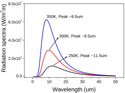
CHAPTER 1Figure 1.1: The blackbody radiation spectra at 350K, 300K, and 250K. The peak
intensity varies from 8.5 μm to 11.5 μm. 3
Figure 1.2: The atmosphere transmittance spectrum. 3
Figure 1.3: The schematic drawing of the type-I, type-II and type-III heterojunction. 7 Figure 1.4: The schematic drawing of the band alignment of GaSb and InAs in GaAs matrix. 8
Figure 1.5: Energy bandgap versus lattice constant of the III-V semiconductor. 9
CHAPTER 2 Figure 2.1: The sketch of Varian/Veeco Gen-II solid source MBE system. 13
Figure 2.2: The RHEED pattern of (a) GaAs film and (b) GaSb QD growth on GaAs substrate. 15
Figure 2.3: The RHEED intensity oscillation of GaAs film growth for Ga growth rate calibration. 17
Figure 2.4: The growth rate versus the beam equivalent pressure of Ga cell. 18
Figure 2.5: The relationship of the doping concentration and cell temperature of silicon dopant cell. 19
Figure 2.6: The setup of PL measurement system. 20
Figure 2.7: The sketch of typical QDIPs device structure. 22
Figure 2.8: The setup of the dark current measurement system. 23
Figure 2.9: (a) The setup of the FTIR measurement system. (b) The 45° waveguide measurement method. 24
Figure 2.11: The noise measurement setup. 26
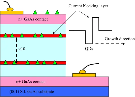
CHAPTER 4 Figure 4.1: The schematic drawing of the device structure used in this study. Inset shows the band diagram of the QDs in the active region. 36
Figure 4.2: The TEM image of the ten InAs/GaAs QDs layers with 50nm barrier. Each barrier includes 47nm GaAs and 3nm Al0.2Ga0.8As. 36
Figure 4.3: The low temperature PL result of the sample. The transition peaks are at 1.11 and 1.17 eV. The ground state FWHM is around 50meV. 37
Figure 4.4: The scatter line shows the dark current activation energy at different voltages, and the straight line shows the kinetic energy of electrons across one barrier under uniform electric field. 38
Figure 4.5: The responsivity versus bias at different temperatures. 39
Figure 4.6: The noise spectrum at 130K and different bias voltages. 40
Figure 4.7: The current gain of the sample at different bias and temperatures. 41
Figure 4.8: The capture probability at different bias and temperatures. 42
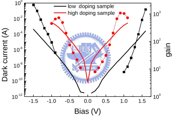
Figure 4.9: The dark current (solid curve) and current gain (scatter curve) curve for the two samples with different doping concentration at 77K. 43
Figure 4.10: The calculated average extra carrier number <N> in one QD at different temperature and voltages. 45
Figure 4.11: The quantum efficiency of the sample at different bias and temperature. 46 Figure 4.12: The quantum efficiency (solid curve) and <N> (scatter line) at different temperatures and negative voltages. The vertical lines are used to indicate the voltage of quantum efficiency peaks. The peak quantum efficiency occurs around <N>=0.4. 47
CHAPTER 5
Figure 5.1: The low temperature (20K) PL result of single layer and multi-layer (vertically aligned ten layers with 10nm spacer). 51 Figure 5.2: The PL spectra of (a) single and (b) multi-layer samples at different
temperature. 52 Figure 5.3: The temperature dependence of the peak energies of the PL spectra. The scatter curves are the experiment data, and the continuous curves are calculated results according to the Varshni law using the parameters (α, β) of InAs. 53 Figure 5.4: The FWHM of single and multi-layer samples at different temperature. 54 Figure 5.5: The cross-section TEM image of the device B. 56 Figure 5.6: The 40K photocurrent response spectra of sample A and B. 58 Figure 5.7: The 77K noise current gain of sample A and B as a function of the average electric field. 59 Figure 5.8: The normalized frequency response of photocurrent of sample A and B at 40K and 0.5V. 60 Figure 5.9: The quantum efficiency of sample A and B at 77K. 61
CHAPTER6
Figure 6.1: The schematic drawing of the device structure used in this study. Inset shows the band diagram of the QDs in the active region. 65 Figure 6.2: The surface AFM image of sample A (1μm×1μm).
Figure 6.3: The normalized photocurrent spectra of these four samples at 40K and 1V. 65 Figure 6.4: The 77K micro-PL and 1.4K PLE spectra of sample A. The inset shows
Figure 6.5: The PLE spectra of the four samples at 1.4K. 69 Figure 6.6: (a) The simulation structure of sample A. (b) The simulated electron states of angular quantum number l=0, 1. 71 Figure 6.7: The six electron states wavefunction. 72 Figure 6.8: The intersubband carrier transition oscillator strength
( a) for Δl=0 (TM polarized), (b) for Δl=1 (TE polarized). 73
Figure 6.9: The photocurrent spectra of sample B at 40K and 1V for different polarization angle of the incident infrared light from the 45° polished facet on the detector. 74 Figure 6.10: The dark current density and responsivity of sample A and D at 77K. 76 Figure 6.11: The quantum efficiency and detectivity of sample A and D at 77K. 76
CHAPTER 7
Figure 7.1: The sample structure of GaSb/GaAs QDs in our study. 80 Figure 7.2: The source shutter operation sequence during GaSb QDs growth. And, the
substrate temperature change procedure. 80 Figure 7.3: The surface AFM image of sample A, B, C, and D. The image size of sample A was 5μm×5μm, and the others were 1μm×1μm. Sample A, B, C and D were with 1, 2, 3 and 4 monolayer GaSb film. 82 Figure 7.4: The surface AFM image of sample E, F, D, and G. The image size of sample E was was 5μm×5μm, and the others were 1μm×1μm. Sample E, F, D and G was grew at 540℃, 520℃, 500℃ and 480℃. 83 Figure 7.5: The surface AFM image of sample H, D, I, and J with the image size
1μm×1μm. The V/III flux ratio is equal to 3, 5, 10 and 20. 84 Figure 7.6: (a) SK mode GaSb/GaAs QDs. (b) IMF mode GaSb/GaAs QDs. There misfit array at the GaSb QDs and GaAS substrate interface. 85
Figure 7.7: The schematic band structure of the GaSb/GaAs heterostructure in different excitation level. 86 Figure 7.8: The 20K PL response spectrum of the sample D at different excitation
power. 87 Figure 7.9: Measured transition energy of sample A vs the cubic root of the excitation power. 88 Figure 7.10: PL emission spectrum of sample D at different temperature at 10mW excitation power. 89
Figure 7.11: The emission peaks energy level of WL and QDs at different temperature. 9 0
Figure 7.12: Product of Fermi-Dirac and Gaussian distribution functions at different temperatures. 90 Figure 7.13: Photoluminescence spectra of (a) sample A and (b) sample B at 20K. 92 Figure 7.14: Measured transition energy versus the cubic root of the excitation power. The interceptions of the extrapolated lines with the y axis give the transition energies at thermal equilibrium. 93 Figure 7.15: Transition energies of quantum wells with 1, 2 and 3 ML of GaSb. The measured result is compared with the theoretical result. 95
CHAPTER 8
Figure 8.1: The sample structure of GaSb on Silicon substrate in our study. 97 Figure 8.2: The surface AFM image of these samples. The image size is 10μm×10μm with the 30nm scale bar. 98 Figure 8.3: The 20K PL response from the 8nm In0.2Ga0.8Sb/GaSb QW. The FWHM
of sample C is 11.2meV and peak is at 0.177eV. 99 Figure 8.4: High resolution XRD (004) rocking curve of GaSb on Silicon. The
FWHM of the sample C is 490 arcsec. 100 Figure 8.5: Cross-section HR-TEM image of the GaSb/AlSb superlattice on Silicon substrate in sample C. In area 1, 2 and 3 the dislocations merge or stop at the superlattice interface. 102
Chapter 1
Introduction
The III-arsenic semiconductors and their related quantum structure have been widely used in optoelectronic and high-speed device application. With the mature heterojunction epitaxy, the quantum well laser diode, the quantum well infrared photodetectors (QWIPs), heterojunction bipolar transistor (HBT), and high electron mobility transistor (HEMT) have been realized [1, 2]. Besides, the self-assembled defect-free 3-D confined InAs/GaAs quantum dot system with S-K (Stranski-Krastanov) mode growth method has also been successfully developed in the past decade. The physics of the quantum dot has been widely studied, and the quantum dot also has been used in many different optoelectronic devices, such as single photon emitter, quantum dot lasers, and infrared detectors [3]. Recently, III-antimonide compounds have been regarded as potential materials for applications in ultra high-speed devices and long-wavelength photonic devices due to their high electron mobility and small band gap energies [4]. Furthermore, the heterostructures composed of antimony and other III-V compounds, such as arsenic, have also been of physical interest because of the unconventional type-II and type-III band alignment
[5-7].
1.1 Infrared technology
Any object with nonzero temperature will emit radiation. The radiation spectrum peak of lower temperature object is at longer wavelength. For the detection of people in the night or the space application, the infrared detection technology is important. In the past two decades, the quantum well made by the III-V material has been widely
used in the infrared detection technology. Furthermore, the quantum dot infrared photodetectors (QDIPs) is regarded as the potential structure to overcome the drawbacks of QWIPs.
1.1.1 Blackbody radiation
All of objects with nonzero temperature generate thermal radiation which could be approximated as a blackbody with an emissivity factor smaller than one. The blackbody is an ideal radiation source, and the radiation spectrum is the function of temperature. The radiation power density spectrum of the blackbody is expressed as:
( )
1
1
2
,
5 2−
⋅
=
hc kTe
hc
T
Q
λλ
π
λ
(1.1)where h is the Plank’s constant, k is the Boltzmann constant, c is the speed of light, λ is the wavelength, and T is the blackbody temperature. Fig. 1.1 shows the blackbody radiation spectra at 350K, 300K, and 250K. The peak intensity wavelength varies from 8.5μm to 11.5μm. The moisture (H2O) and carbon dioxide (CO2) in atmosphere
will absorb the infrared. Therefore, the infrared transmittance spectrum of the atmosphere is not flat. Fig. 1.2 shows the transmittance spectrum of atmosphere. There are two transparent windows of infrared: 3~5μm (MWIR) and 8~13μm (LWIR). Therefore, the detection wavelength of infrared detectors which are used on earth must fall in the transparent window. For the space application, all of the detectors with different detection wavelength can be used due to the vacuum environment.
1.1.2 Infrared detection technology
There are two major detection types of the infrared radiation: thermal and photon detector. The detection mechanism of thermal detector is the physics characteristics
0 10 20 30 40 50 0.0 2.0x10⁷ 4.0x10⁷ 6.0x10⁷ 8.0x10⁷ 300K, Peak ~9.5um 250K, Peak ~11.5um
Radiation spect
ra (W
/m
2m)
Wavelength (um)
350K, Peak ~8.5umFigure 1.1: The blackbody radiation spectra at 350K, 300K, and 250K. The peak intensity varies from 8.5μm to 11.5μm.
change after the absorption of infrared radiation, such as resistance, thermoelectric, and charge. Bolometers and microbolometers are based on the resistance change. Thermocouples and thermopiles use the thermoelectric effect. In general, the thermal detector could be operated at higher temperature, but the response time is much longer due to the limitation of the thermal conductivity.
There are three types of the photon detectors, including QWIPs (or QDIPs), II-VI photodiodes, and type-II InAs/GaSb superlattice photodiodes. The operation of the photon detectors is based on the carrier transition from lower energy state (valence band) to higher energy state (conduction band) and becomes free carrier. The free carrier (electron) concentration increase causes the photo current increase. The major advantage of the photon detector is the shorter response time than thermal detector because the carrier transition process is faster than the physics property change. However, the photon detectors must be operated at low temperature in order to reduce the thermal noise. The advantages and limitations of these three type detectors are listed in table 1.1 [8].
Detector type Advantages Limitations
QWIPs Mature III-V technology
Large, uniform FPA
High dark current Low quantum efficiency Non-normal absorption
II-VI (MCT) High detectivity
High quantum efficiency Low dark current
High device defect Expensive substrate Epitaxy difficulty
InAs/GaSb SLS High detectivity
High quantum efficiency
High dark current Epitaxy difficulty
The major advantages of QWIPs are the mature III-V epitaxial technology and large area uniformity, which is important for the focal plane array (FPA) application. However, the high dark current, low quantum efficiency, and the non-normal incident Table 1.1: Advantages and limitations of different type infrared detectors.
radiation absorption limit the device performance.
1.1.3 Overview of QWIPs and QDIPs
The intersubband infrared absorption of the GaAs/AlGaAs QW was first observed by West and Eglash in 1985 [9]. The absorption peak at 8μm and 10μm was observed in the 65Å and 82 Å GaAs/AlGaAs QW. Two years later (1987), the first QWIPs device was demonstrated by Levine et al. [10]. The absorption of the 65 Å GaAs/AlGaAs QW was 10.8μm with a responsivity of 0.52 A/W. In 1991, the first 128×128 GaAs/AlGaAs QWIP FPA was fabricated [11]. In 2003, the large 640×514 four detection bands IR FPA with 99.9% of the pixels working was fabricated by JPL
[12]. However, the operation temperature of QWIPs is difficult to further increase and the device is insensitive for the normal incident radiation. These drawbacks limit the application of QWIPs.
After the high quality self-assembled quantum dot (QD) epitaxial technology was carried out, the QD is assumed as potential active layer structure for the intersubband infrared detector application. Due to the three dimensional confinement of the carrier, the QDIPs are sensitive to normal incident infrared radiation. And, because of the discrete energy level of the QD, the carrier intersubband relaxation time is much longer than that of QW. The longer relaxation time would enhance the device current gain and reduce the detector noise. Thus, the QDIPs are of the great potential to surpass the disadvantages of the QWIPs [13].
The infrared absorption of the QDs had been observed by different method in different groups. Drexler et al. studied the intersubband far-infrared absorption by a capacitance spectroscopy technique coupled with a far-infrared spectrometer [14]. Phillips et al. reported the far-infrared absorption of Si-doped InAs QDs by Fourier Transform Infrared (FTIR) spectrometer [15]. Berryman et al. studied the
mid-infrared intersubband absorption in InAs QDs by photo conductivity measurement method [16]. And, Chua et al. investigated the polarization dependence of the intersubband absorption in InAs QDs by a FTIR spectrometer [17].
In 1998, several reports of the InAs/GaAs QDs as active structure intersubband photoconductive detectors were published. Phillips et al. measured the 17μm photo response signal by a FTIR and a low-noise amplifier measurement system [18]. Maimon et al. demonstrated the responsivity signals in the different polarization infrared radiation, and the carrier transition states were also studied [19]. Pan et al. showed the response signals were from E0 to E1 (13μm) and E0 to E2 (11μm), and this
device showed a peak detectivity of 1×1010 cm-Hz0.5/W at 40K [20]. Xu et al. studied the electro-optic characteristics of the QDIPs, and showed the ratio of TE (s-polarization) and TM (p-polarization) mode [21].
Except for the typical vertical QDIPs, the lateral QDIPs, which carriers transport direction is perpendicular to growth direction, had been also studied [22]. The lateral QDIPs was predicted of higher responsivity than vertical QDIPs due to the higher current gain. However, the lateral QDIPs was more difficult to fabricate the FPA, because the two electric contact pads were fabricated at the same side.
In 2001, the performance of the QDIPs was improved by inserted the high band gap material (AlxGa1-xAs) in the active region to reduce the device dark current and
increase the device performance. Wang et al. demonstrated the low dark current and high detectivity (2.5×109 cm-Hz0.5/W at 77K, ~6μm) QDIPs by capping a thin Al0.2Ga0.8As layer after the QDs [23]. Chen et al. compared two different structures:
the InAs QDs surrounded by GaAs or AlAs/GaAs super lattice. The ratio of Ipc/Idark of
latter structure showed more than two orders higher than former one [24]. Stiff et al. used a single Al0.3Ga0.7As barrier as current blocking layer to reduce the dark current
operated up to 150K. With the different active structure design, encouraging results have been demonstrated with operation temperatures over 200K [26-28] and even up to room temperature [29, 30]. The 640×512 pixels long wavelength (8.1μm) QDIP FPA has fabricated in 2007 by Gunapala et al [31]. The noise equivalent temperature difference is of 40mK at 60K operation temperature.
1.2 GaSb/GaAs quantum structure and GaSb growth on Silicon
substrate
1.2.1 Semiconductor heterojunction
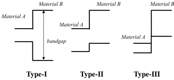
A heterojunction is the junction of two different semiconductor materials with different bandgap energy. In the ideal case, the interface is strain-free and the bandgap energy is not changed. Due to the bandgap energy, the work function, and the electron affinity difference in different material, the heterojunctions have three kinds of band alignment, including type-I, type-II and type-III [32, 33]. Fig. 1.3 shows the ideal case energy band alignment of these three kinds of heterojunction. By controlling the composition of the group-III and V in ternary or quaternary semiconductor, we can adjust the band alignment in the heterostructure device.
Type-I Type-II
Type-III
Material A Material B Material A Material B Material B Material A bandgap
Figure 1.3: The schematic drawing of the type-I, type-II and type-III heterojunction.
The quantum wells and self-assembled quantum dots made by GaSb or InAs embedded in GaAs matrix show the different band alignment. The former is the type-II band alignment, and the later is the type-I. The major difference of the type-II and type-I band alignment is the spatially separate electrons and holes. Fig. 1.4 shows the GaSb and InAs quantum structure embedded in GaAs matrix band alignment system. The spatially separate electrons and holes will result in longer carrier life time.
1.2.2 GaSb base optical and electronic devices
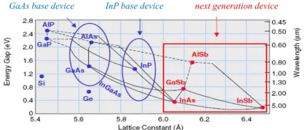
The Sb-base device has the advantages of narrow band gap and high electron mobility over conventional GaAs or InP base devices [34, 35]. Fig. 1.5 shows the band gap energy versus lattice constant. The Sb-base (red rectangular) is the next generation of the long wavelength laser diode and high speed device application. The GaSb based laser diode can emit mid-infrared (2~5μm) region with different structure. The type-I InGaAsSb/AlGaAsSb quantum well emits at the 2~2.6μm region. The type-II InGaAsSb/GaSb, type-III InAs/InGaSb, and InAl/InGaSb/AlSb, which are all based on GaSb substrate, can emit beyond 2.6μm. Moreover, the Sb based HEMTs
GaSb in GaAs matrix
Type-II band alignment
GaAsGaSb GaAs InAs
InAs in GaAs matrix
Type-I band alignment
Figure 1.4: The schematic drawing of the band alignment of GaSb and InAs in GaAs matrix.
and HBTs can attain higher operation frequency and lower noise. The HEMTs with InAs or InSb-QW channel on GaSb substrate shows the much higher operation frequency than the GaAs/AlGaAs HEMT devices.
The Sb-base devices are grown on GaSb substrate, but the substrate is expensive. Thus, the cheaper GaAs substrate is used for the Sb-base device with a thick AlSb buffer layer. Furthermore, the silicon substrate is much cheaper and more hardness than GaAs substrate. In recent years, the growth of GaSb on Silicon substrate was reported by K. Akahane et al. [36] and G. Balakrishman et al. [37].
1.3 Organization of the Thesis
The thesis is separated into two parts: one is the QDIPs device based on the InAs/GaAs QDs (chapter 3, 4, 5, and 6), and the other is the GaSb material study (chapter 7 and 8). Due the high current gain of the QDIPs, the device can be operated at higher temperature and even up to room temperature. However, only a few studies are executed to study the high gain behavior. Besides, the lower quantum efficiency is still a drawback in the device application. In our study, we try to increase the quantum
GaAs base device InP base device next generation device
efficiency and enhance the roll-off frequency at the same time by using the vertically coupled QDs in the active layer. Furthermore, the carrier intersubband transitions will influence the quantum efficiency, photocurrent spectra, and transition oscillator strength. These topics are also studied in the thesis. In addition to the QDIPs, the GaSb material is also studied. The Sb-based semiconductor is regarded as the potential material to execute the higher speed device and longer wavelength laser. Two studies are executed in this thesis, including GaSb/GaAs QDs and the GaSb growth on silicon substrate.
In chapter 2, the experimental techniques are described, including molecular beam epitaxy (MBE) system, analysis techniques (AFM, PL, and XRD), QDIPs device processing, and QDIPs measurement system.
In chapter 3, the fundamentals of QDIPs are described. The intersubband absorption, quantum efficiency, current gain, responsivity, dark current, noise, and detectivity are discussed.
In chapter 4, the temperature dependent responsivity of QDIPs is discussed. The responsivity of QDIPs shows a very different behavior compared to that of QWIPs. In QWIPs, the responsivity keeps almost constant at different device temperatures and changes linearly with the bias voltage. On the contrary, in QDIPs, the responsivity increases dramatically with both voltage and temperature. Only few studies were executed with the experimental data. In this chapter, a detailed analysis of the responsivity was done based on the current gain measurement to explain the responsivity temperature dependent behavior in QDIPs.
In chapter 5, the vertically coupled QDIPs were studied. The performance of QDIPs is limited by the low quantum efficiency which is critical to the performance. In addition to quantum efficiency, poor frequency response of the responsivity in QDIPs was also reported with the roll-off frequency lower than 1K Hz especially at
lower temperatures. The roll-off frequency of QDIPs is a few orders of magnitude lower that of QWIPs. The long RC time constant originated from the charging process of the electrons into the quantum dots deteriorates the frequency response. This phenomenon limits the use of QDIPs in some military and space applications where the high speed detection is needed. In this chapter, the vertically coupled QDs were used as the active layer in the QDIPs to solve the issues mentioned above.
In chapter 6, the QDIPs with an additional thin Al0.2Ga0.8As layer near the QDs
were studied. With the thin Al0.2Ga0.8As layer, the carrier transitions of the QDIPs
could be engineered. One of the transitions of the simple InAs/GaAs QDIPs would be suppressed. Thus, a much narrow photocurrent spectrum was observed when the Al0.2Ga0.8As layer is closer to the QDs. The fractional spectra width was reduced to
only 10% and enhanced the quantum efficiency. The thin Al0.2Ga0.8As layer also
reduces the device dark current, and enhances the device performance.
In chapter 7, the self assembled GaSb QDs embedded in GaAs matrix were studied. The GaSb/GaAs QDs show a type-II band alignment in which the electron and hole is spatially separated. The morphology of the surface QDs and photoluminescence of the embedded QDs at different excitation power and temperature were studied. Furthermore, the valence band offset (VBO) between GaSb and GaAs has been studied by the observation of discrete monolayer light emission.
In chapter 8, the GaSb material growth on Silicon substrate with different buffer layer structure was studied. The GaSb crystal quality and In0.2Ga0.8Sb QW photo
emission intensity was analyzed by x-ray diffraction and photoluminescence, respectively. The sample with superlattice buffer layer structure shows the best quality.
Chapter 2
Experimental Techniques
In this chapter, the experimental techniques used in my experiment are presented. It consists of three parts: molecular beam epitaxy (MBE) system for sample growth, the material characterization analysis techniques, and quantum dot infrared photodetectors (QDIPs) processing and measurement.
2.1 Molecular Beam Epitaxy
2.1.1 Introduction to our MBE system
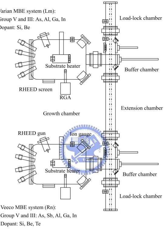
The epitaxial system in our laboratory consists of two growth units. One is Varian Gen-II system, and the other is Veeco Gen-II system. These two growth units are linked by an extension chamber. Fig. 2.1 shows a sketch of the integral MBE system. Each system consists of three ultra high vacuum (UHV) chambers, including growth chamber, buffer chamber and load-lock chamber. The buffer chamber is connected to the other two chambers and isolated by gate valve.
The pumps used in our MBE system is oil-free pumps for reduce the contamination. In order to maintain UHV, croy-pump, ion-pump, and titanium sublimation pump (TSP) are used in growth chamber, ion-pump and TSP pump are used in buffer chamber, and croy-pump is used in load-lock chamber. Besides, in order to pump down the system from atmospheric pressure, a scroll and turbo-molecular pump is connected to these three chambers and isolated with three all metal angle valves.
One of the integral MBE systems is called Lm-MBE (Varian Gen-II), and the other is called Rn-MBE (Veeco Gen-II). The Lm-MBE system consists of eight sources. There are arsenic (As) cracker cell for group-V source and aluminum (Al) cell, gallium (Ga) cell, and indium (In) cell for group-III source. Besides, the silicon
Varian MBE system (Lm): Group V and III: As, Al, Ga, In Dopant: Si, Be
Veeco MBE system (Rn):
Group V and III: As, Sb, Al, Ga, In Dopant: Si, Be, Te
RGA Substrate heater RHEED gun RHEED screen Ion gauge Load-lock chamber Load-lock chamber Buffer chamber Buffer chamber Extension chamber Substrate heater Growth chamber
(Si) cell and beryllium (Be) cell are used for different doping. In additional to the sources in Lm-MBE system, the group V material (antimony: Sb) valve cracker cell and a tellurium (Te) cell for n-type doping are added in Rn-MBE system.
Two temperature control zones of the group V valve cracker cell of As and Sb, bulk and cracking zone, are controlled by individual filament. The bulk zone of As is usually operated between 350℃ and 400℃. This cell can be operated at different mode to supply As2 or As4 by controlling the cracking zone temperature varying from
840℃ to 500℃. The beam equivalent pressure (BEP) is controlled by the needle valve. The bulk zone of Sb is operated between 500℃ and 600℃, and the cracking zone is operated at 1050℃ to supply the Sb. Two designs are used for the group III source cell, including Kundsen cell (K-cell) and SUMO cell. The SUMO cell has two filaments to control bulk and tip zone. We keep the tip temperature and vary the bulk temperature to control the beam flux. The K-cell only has one filament to control the beam flux. The group III Ga and In source are hot lip design and Al is cold lip design due to the different material characteristic.
There are two analysis instruments in the growth chamber. One is residue gas analyzer (RGA), and the other is the reflection high energy electron diffraction (RHEED) monitor. The RGA is used to analyze the residue gas in the chamber. The RGA monitor can also serve as leakage detector by keeping the detection range of the atomic mass unit (AMU) to helium (He, 4). The helium gas is usually used to detect the chamber leakage, due to the small size of atom and little amount in atmosphere. The RGA monitor is a very sensitive leakage detector, but it can only be operated when the chamber at ultra high vacuum (pressure lower than 1×10⁻⁸ torr). The RHEED allows us to in-situ monitor the surface reconstruction structure. By using a high energy electron beam with an angel, the reconstruction structure of the sample surface (typically a few monolayers) can be analyzed with the diffraction patterns. It
makes the substrate surface native oxide desorption easy. It indicates the oxide free surface when the surface reconstruction pattern appeared. Besides, it is useful for quantum dot (QD) growth by observing the RHEED pattern transition. When the growth mode changes from layer to dot, the RHEED pattern will change from streaky to spotty pattern. Fig. 2.2 (a) (b) shows the layer and dot RHEED pattern. Also, by observing the RHEED pattern intensity oscillation period, we can calibrate the material growth rate. The growth rate calibration will be discussed later.
2.1.2 Pre-growth procedure
In order to maintain the chamber cleanness and obtain high quality epitaxial film, a standard treatment procedure for wafer before growth is important and necessary. The epi-ready substrate is mounted on indium free Mo spring substrate holder, and then put into load-lock chamber. In load-lock chamber, the wafer will be baked at 200℃. The moisture on wafers and sample holders will be baked out during the bake process. These wafers will be transferred to buffer chamber when the load-lock chamber pressure lower than 1×10⁻⁸ torr after bake out and pump down process. The each wafer will be baked up to 400℃ more than 4 hours in buffer chamber in order to Figure 2.2: The RHEED pattern of (a) GaAs film growth, and (b) GaSb QD growth
on GaAs substrate.
remove the organic species. Usually, the cleanness of wafers is judged by the chamber pressure (chamber pressure must be lower than 3×10⁻⁹ torr). After the 400℃ bake process, the wafer can be transferred to growth chamber to grow. A thin native oxide exists on the substrate surface when the substrate exposure at atmosphere. The native oxide will not be removed during the bake process in load-lock and buffer chamber. Before growth, the native oxide of substrate is desorbed by heating the wafer up to the suitable temperature under arsenic phase. The desorption temperature depends on the substrate type. The desorption temperature is 610℃ for GaAs and 510℃ for InAs substrate.
Our MBE system is served as III-V semiconductor material growth. But, we also use the silicon substrate for sample growth. The native oxide of silicon is hard to remove by heating in our system. The native oxide of silicon must be removed before loading. We use diluted HF solution to clean the silicon substrate, and load it into load-lock chamber as soon as possible to prevent the native oxide formation. The followed pre-growth procedure is 200℃ bake in load-lock chamber, and 500℃ in buffer chamber. Before growth, the silicon wafer is heated up to 800℃ (substrate thermal couple temperature, it is our system limit).
During the sample growth, the growth chamber is cooled down by continuous liquid nitrogen flow. The cooled cryo panel in growth chamber is served as a powerful absorption pump to maintain the system vacuum.
2.1.3 Growth rate and doping concentration check
In general, we use the RHEED intensity oscillation on non-rotate substrate to calibrate the group-III material (Al, Ga, In) growth rate. A GaAs wafer with (001) orientation is used to check the Al and Ga cells growth rate, because the AlAs (5.66 Å) and GaAs (5.65Å) have almost the same lattice constant. Besides, the InAs wafer with
(001) orientation is used to check In cell growth rate. Fig. 2.3 is the RHEED intensity oscillation of Ga cell. One oscillation period means one monolayer of GaAs.
For carefully designed source cell, a fixed cell temperature gives a stable source beam flux. We use a beam flux monitor ion gauge to measure the source beam equivalent flux pressure (BEP). In Varian (Veeco) Gen-II MBE, the beam flux monitor gauge and substrate holder can exchange their location exactly by rotating the substrate manipulator (CAR). First, we measure BEP at different temperature of each cell. Then, we measure the RHEED intensity oscillation at different cell temperature. The growth rate is determined by the oscillation period. Finally, we can get the relationship between the BEP and growth rate. Fig. 2.4 shows the growth rate versus the beam equivalent pressure of Ga cell. We can see that the growth rate and the BEP have very good linear dependence. Before each sample growth, the desired growth rate is obtained by adjusted the cell temperature to reach the corresponding BEP.
Figure 2.3: The RHEED intensity oscillation of GaAs film growth for Ga growth rate calibration.
When sample growth, the substrate will rotate in order to obtain uniform material composition and flat heterointerface in the whole wafer. However, the wafer would not rotate during the growth rate calibration.
Under 1μm/hr growth rate, the n-type (Si, Te) and p-type (Be) doping concentration for GaAs are calibrated with the etched C-V or Hall measurement for several temperature of the dopant cells. We assume the evaporated amount of the dopant material is the stable at different cell temperature, because the BEP of dopant material is not detectable of our beam flux monitor gauge. Fig. 2.5 shows the relationship between cell temperature and doping concentration of n-type silicon doping. During sample growth, the doping concentration for a definite growth rate can be calculation easily. y = 3.702766E-07x + 3.627270E-09 R2 = 9.997026E-01 0.0E+00 1.0E-07 2.0E-07 3.0E-07 4.0E-07 5.0E-07 0 0.2 0.4 0.6 0.8 1 1.2 1.4 Ga K GR B eam fl ux
2.1.4 Growth condition
The group-V/group-III BEP ratio must be kept at suitable range for high quality epitaxial material. The typical V-III ratio is 10~20 for III-arsenic and 2~5 for III-antimonide. In general, the suitable growth temperature for 2-D layer of AlAs, GaAs, InAs, GaSb, and InSb are about 600℃, 580℃, 500℃, 500℃ and 450℃, respectively. However, for the 3-D structure (InAs or GaSb quantum dots), the QDs characteristics (size and density) is highly dependent on the growth conditions, including III/V ratio, temperature, and growth rate.
2.2 Material Characteristics Analysis
2.2.1 Atomic Force Microscope
The Veeco D3100 tapping mode atomic force microscope (AFM) system is used in our study. A QD layer is grown on the sample surface with the same growth condition with the active layer QDs for AFM study. By the AFM study, the density of
y = -3.766898E-05x + 1.318217E-03 R2 = 9.999777E-01 6.20E-04 6.40E-04 6.60E-04 6.80E-04 7.00E-04 7.20E-04 16.8 17 17.2 17.4 17.6 17.8 18 18.2 log(concentration) 1/(temp+273.15)
Figure 2.5: The relationship of the doping concentration and cell temperature of silicon dopant cell.
QDs can be obtained. However, due to the capping layer different (no capping layer on the surface QDs), the size of QDs is not the same. By cross-section transmission electron microscope (TEM) study, the size of the surface QDs is larger than the embedded layer QDs.
2.2.2 Photoluminescence
Photoluminescence (PL) is a useful non-destructive optical technique for analyzing the semiconductor material characteristics. The impurity level, defects, band gap and crystal quality will be obtained in the PL study. We use an Argon laser to generate electron-hole pairs in the material. The emission occurs when the electron-hole pair recombines. Fig. 2.6 shows the schematic drawing of the PL measurement system. In our conventional PL system, the laser spot size is about 50μm in diameter. When the excitation power density increase, the laser will heat the sample. In order to obtain the high power density information, we use micro-PL system, which laser spot size is about 2μm in diameter, to increase the excitation power density and avoid the heating effect.
Ar
+laser
TRIAX 550 monochromator DUTlock-in Amplifier
detector temp. sensor chopper2.2.3 X-Ray Diffraction Analysis System
The Bede D1 high resolution X-Ray diffraction meter (HRXRD) system is used to measure the crystal structure information, such as lattice constant and layer composition. We use the high resolution ω-2θ scan mode to measure the GaSb epi-layer on silicon substrate quality. In general, we measure the GaSb (004) curve full width at half maximum (FWHM) to analyze the epitaxial film quality.
2.3 QDIPs Device Process and Measurement
Unlike the QWIPs, no grating is fabricated on the device surface. We measure the normal incident absorption characteristics. The QDIPs device fabrication is done by standard lithography, wet etching and metallization process. The device mesa size is 370μm×260μm with a 200μm×200μm square light window. Fig. 2.7 shows the standard QDIP device structure and the inset shows the top view of the device after processing. The wet etching solution is H2SO4: H2O2: H2O=1: 8: 80, and the etching
rate is about 80 Å/sec for GaAs epitaxial layer. The n-type ohmic contact metal is Ni/Ge/Au (300Å/700Å/3000Å) evaporated by single E-gun evaporation system at the top and bottom of the mesas. The bottom contact is referred as ground contact in all measurement. A good ohmic contact can be obtained by a rapid thermal annealing at 380℃ for 30 sec. After processing, the device is mounted on a holder with good thermal conductivity and connected to electric feedthrough by gold wire bonding. The QDIPs package is cooled with close cycle helium refrigerator for different temperature measurement.
Three important characteristics of QDIPs device are measured to judge the device performance, including dark current and 300K background photocurrent, device absorption spectrum and responsivity, and device noise level and detectivity.
In our laboratory, the Keithley 236 is used to measure the dark current and background photocurrent. The cryostat is used to measure the background photocurrent at different temperature. Besides, we put the sample at the air phase of liquid helium dewar flask and a temperature sensor is mounted near the sample. By controlling the distance between the sample and liquid helium surface, we can measure the dark current at different temperature. Fig. 2.8 shows the dark current measurement system setup.
Normal incident light
(001) S.I. GaAs substrate n+ GaAs contact n+ GaAs contact QDs AlGaAs Bottom con tact Top contact Light window mesa
Figure 2.7: The sketch of typical QDIPs device structure and the top view of the device after processing.
The second important characteristic is the responsivity spectrum. In our laboratory, the Fourier transform infrared spectroscopy (FTIR) is used to measure the photocurrent spectrum. Fig. 2.9 (a) shows the FTIR measurement system. The FTIR method is faster to get the spectrum than the monochromator method. The FTIR used in our lab is Nicholet 550 with computer control. The response photo signal is amplified by a low noise current amplifier (SR570) and feed back to the FTIR. Fig. 2.9 (b) shows the 45° waveguide measurement method. The incident light is polarized by a polarizer. The 0° polarized light included 50% TM and 50% TE mode light, and the 90° polarized is totally TE mode light. This method can measure the device photocurrent sensitivity under different polarization of radiation.
Keithley 236
Temp. sensor
device Dewar
liquid helium
Because the light source of FTIR is not calibrated, we use a blackbody and lock-in amplifier to measure the photocurrent and calculate the absolute responsivity. The setup is showed in Fig. 2.10. In order to avoid the interband photocurrent, the germanium filter is used to filter out the high energy photon. Typically, the chopper frequency is set as 1000Hz in our measurement.
(a)
DUT Temp. sensor FTIR (Nicolet 550) SR570 Current amplifierGrowth direction
(b)
S
P
Incident radiationFigure 2.9: (a) The setup of the FTIR measurement system. (b) The 45° waveguide measurement method.
The peak responsivity (Rpeak) can be calculated by the following equation:
λ
Qd
R
E
T
T
MF
A
I
R
ZnSe Ge D p peak⋅
⋅
⋅
⋅
⋅
⋅
=
∫
(2.1)where the Ip is the photocurrent, AD is the device area. MF is the modulation factor of
the chopper, and it is 0.38 in our system. T is the transmission coefficient of Ge filter and ZnSe window, and it is 0.64 and 0.7. R is the normalized response spectrum which is obtained by FTIR. Q is the blackbody radiation spectrum. E is the configuration factor given by:
⎥
⎥
⎦
⎤
⎢
⎢
⎣
⎡
⎟
⎠
⎞
⎜
⎝
⎛
+
⎟
⎠
⎞
⎜
⎝
⎛
=
2 2 22
2
d
D
d
E
(2.2)where d is the aperture size of the blackbody radiation source and D is the distance between the light source and the device. The relation between applied bias and peak responsivity can be obtained.
The third important characteristic is the detectivity. The detectivity is the normalized signal to noise ratio. We use the SR770 fast Fourier transform (FFT) spectrum analyzer to measure the noise level. In order to reduce the noise which
Temp. sensor Black body 1000℃ DUT SR570 Current Amp. SR 830 Lock-in Amp. Ge filter chopper ZnSe window
comes from the environment, we put the sample in the air phase of the liquid helium dewar flask and use the BNC cable for signal connection. Fig. 2.11 shows the measurement setup.
We measure the root mean square noise voltage of QDIP device. The noise current (In)
can be calculated by the following equation.
2 2 2 0 2 n n n
V
A
I
V
=
+
(2.3)where Vn is the measured noise voltage, Vn0 is the noise under open circuit, and A is
the gain of the SR570 current amplifier. After the noise current measurement, we can calculate the detectivity of the device. The detectivity (D*) can be calculate by the following equation. n D
i
B
A
R
D
*=
(2.4)where the R is the responsivity, AD is the device area, the B is the bandwidth, and the
in is the noise current.
SR570
Current amplifier
Temp. sensorSR770
FFT analyzer
Dewar liquid heliumChapter 3
Fundamental of Quantum Dot Infrared
Photodetectors
The quantum dot infrared photodetectors (QDIPs) structure consists of multi layer In(Ga)As/GaAs QDs as the active structure, which is sandwiched by two silicon n+ doped contact layer. A high band gap AlxGa1-xAs current blocking layer is added in
the active layer to reduce the dark current and enhance the performance. The detection mechanism is based on the carrier (electron) transition from lower energy level to higher energy level by absorbing a photon. The carrier at higher energy level is swept out by the external electric field and form the photocurrent. In this chapter, we will discuss the fundamental physics of the QDIPs, including the intersubband absorption (α), quantum efficiency (η), current gain (g), responsivity (R), dark current (Id), noise
current (in), and detectivity (D*).
3.1 Absorption of Intersubband Transition
The absorption coefficient (α) is defined as incident photo energy (ħω) times the number of transitions per unit volume per unit time divided by the incident power per unit area. The absorption coefficient of a given transition from initial state (i) to final state (f) can be expressed as:
(
)
(
i f)
if if dn
n
f
c
m
ne
N
⋅
−
⋅
⎥
⎥
⎦
⎤
⎢
⎢
⎣
⎡
Γ
+
−
Γ
=
* 2 2 2)
(
ω
ω
ε
π
ω
α
=
=
=
(3.1) where ħ is the Plank constant, Nd is the number of dot per unit volume, n is therefractive index, ε is the permeability, ni and nf are the occupation probability in initial
oscillator strength is a dimensionless quantity to express the transition probability from initial state (i) to final state (f). The oscillator strength could be expressed as:
(
)
2 2 *2
f
r
i
E
E
m
f
if=
⋅
f−
i⋅
=
(3.2)3.2 Quantum Efficiency
The quantum efficiency (η) is the photo carrier generation probability. The photo carrier generation process consists of the carrier transition from lower energy level to higher energy level and the excited carrier escape from quantum dot bound state to continuous state. Thus, the quantum efficiency could be expressed as:
e
p
⋅
=
η
αη
(3.3)where the ηα is the absorption quantum efficiency, and pe is the escape probability.
The absorption quantum efficiency (ηα) can be given as:
(
)
(
)
χ
η
αα
=
1
−
r
1
−
e
−2 L (3.4) where r is the reflection coefficient, α is the absorption coefficient, L is the height of the QD, and χ is the polarization correction factor.The escape probability is the function of applied external electric field. The escape probability can be expressed as:
1
1
−⎟⎟
⎠
⎞
⎜⎜
⎝
⎛
+
=
c e ep
τ
τ
(3.5) where the τe is the time which is required to escape from the origin quantum dot, andτc is the excited carrier recapture time. The τe is a function of the electric field and τc is
3.3 Current Gain
The current gain (g) is defined as:
t life
g
≡
τ
τ
(3.6) where τlife is the life time of the photo carrier, and τt is the transit time of the photocarrier across the active region. The current gain can also be expressed as:
c c
NFp
p
g
2
1
1
−
=
(3.7)where the pc is the capture probability when the carrier pass through the QDs, N is the
QDs layer number of the device, F is the filling factor of QDs in one layer. The capture probability is determined by device structure, material parameter, and energy distribution of electrons.
3.4 Responsivity
The photocurrent (Ip) of the QDIPs device can be expressed as:
g
q
A
I
p=
DΦ
η
(3.8) where AD is the device area, q is the charge of electron, Φ is the radiation flux, η is thequantum efficiency, and g is the current gain. The reponsivity is defined as the photo current under unit radiation power. Thus the responsivity can be given as:
g
m
g
q
A
I
R
D pη
λ
μ
η
ω
ω
1
.
24
)
(
=
=
Φ
=
=
=
(3.9)3.5 Dark Current
The dark current of the QDIPs could be divided into three parts:
1. Thermionic emission: the leakage current caused by the carriers which are thermally excited into continuous state and form the current by the external electric field.
2. Thermally assisted tunneling: the leakage current caused by the carriers which are thermally excited into higher energy level and tunnel through the triangular barrier.
3. Temperature independent tunneling: the leakage current caused by the carriers in ground state tunnel into the neighbor QDs state level or into the continuous level. The dark current density can be expressed as:
n
qv
j
D=
d (3.10) where n is the free carrier density, and vd is the carrier drift velocity.3.6 Noise
There are two major noise source of a photodetector under operation. One is the dark noise and the other is the 300K background radiation noise. The dark noise includes thermal noise (Johnson noise), flick noise (1/f noise), and generation-recombination noise (G-R noise). The thermal noise current (ith) is
the electronic noise generated by the thermal agitation of the electrons, and can be expressed as: res th
R
kTB
i
=
4
(3.11)where Rres is the differential resistance of the device, and the B is the measurement
The flick noise is a type of electronic noise of low-frequency phenomenon. The flicker noise current (i1/f) can be expressed as:
f
B
KI
i
f 2 1=
(3.12)where K is a proportionality factor, and I is the bias current.
The G-R noise is a type of electrical signal noise caused by the fluctuation of the generation and recombination of electrons in semiconductor-based photon detectors. The G-R noise current (iG-R) can be expressed as:
(
2 2)
01
2
τ
ω
τ
+
=
−N
B
I
i
G R (3.13)where τ is the lifetime of free carriers, and N0 is the total number of the free carriers of
the device. In QDIPs, the free carrier (N0) is given as:
q
I
N
=
⋅
τ
t0 (3.14)
where the τt is the transit time when the carrier across the device. Thus, the G-R noise
can be express as:
2 2
1
4
τ
ω
+
⋅
=
−B
qIg
i
G R , dg
τ
τ
≡
(3.15)where g is the noise current gain. In most case, the ωτ<<1, thus the G-R noise can be rewritten into:
qIgB
i
G−R=
4
(3.16)As a good approximation, the photoconductive gain and the noise gain are equal in a conventional photoconductor and can be expressed as [38]:
qI
i
g
G R4
2 −=
(3.17)The thermal noise is significant in very low bias region, and the flicker noise is low frequency phenomenon. Therefore, the noise current of QDIPs is primary G-R noise.
Because the G-R noise is the dominated noise of the QDIPs, the background radiation noise can be written as:
gB
qI
i
nb=
4
b , b bg
P
bq
P
R
I
=
⋅
=
(
η
)
⋅
ω
=
(3.18)where Pb is the incident background optical power and can be expressed as:
( )
λ
λ
λ λQ
d
A
P
b D⎟
∫
⎠
⎞
⎜
⎝
⎛ Ω
=
2 12
sin
2 (3.19) where Ω is the field of view, Q is the blackbody radiation power distribution. The integration range is the spectral range of the detector. Therefore, the overall noise is the combination of the dark noise and background noise:⎥
⎦
⎤
⎢
⎣
⎡
⎟
⎠
⎞
⎜
⎝
⎛
⋅
+
⋅
=
+
=
ω
η
=
b d nb nd nP
qg
I
qgB
i
i
i
2 24
(3.20)3.7 Detectivity
For a photodetector, the detectivity (D*, D-star) is used to characterize the device performance. The detectivity equals to the reciprocal of noise equivalent power (NEP), normalized to unit area and unit bandwidth.
(
)
NEP
B
A
D
D 2 1 *=
(3.21) The NEP is the incident radiant power which gives rise to signal current equal to the noise current. The detectivity of QDIPs can be given as:n D