國立交通大學
電信工程研究所
碩士論文
針對長期演進技術系統的多頻帶天線微小化設計
A MINIATURIZED MULTI-BAND ANTENNA
SUITE FOR THE LONG TERM EVOLUTION SYSTEM
研究生:林子淵
指導教授:周復芳教授
針對長期演進技術系統的多頻帶天線微小化設計
A MINIATURIZED MULTI-BAND ANTENNA
SUITE FOR THE LONG TERM EVOLUTION SYSTEM
研究生:林子淵 Student:Tzu-Yuan Lin
指導教授:周復芳 Advisor:Christina F. Jou
國立交通大學
電信工程研究所
碩士論文
A ThesisSubmitted to Department of Computer and Information Science College of Electrical Engineering and Computer Science
NationalChiaoTungUniversity in partial Fulfillment of the Requirements
for the Degree of Master of Science In Communication Engineering
July2011
Hsinchu, Taiwan, Republic of China
I
針對長期演進技術系統的多頻帶天線微小化設計
研究生:林子淵
指導教授:周復芳 博士
國立交通大學電信工程研究所碩士班
中文摘要
第一個天線是設計為雙頻帶微小化天線,主要是要涵蓋長期演進系統所要
求的 698MHz 到 960MHz 和 2300MHz 到 2690MHz 這兩個頻帶。天線架
構是以共平面波導饋入的方式設計,首先先設計一天線主體架構以符合低
頻帶的要求,再透過改變電流路徑和接地金屬面的方式以提供雙頻頻帶和
提高高頻增益值。
第二個天線則是進一步涵蓋 1710MHz 到 2170MHz 頻帶而設計為三頻帶天
線。天線架構以微帶線饋入的方式設計,與第一個天線相同的是,一開始
先設計天線主體架構以符合低頻頻帶的要求,並使用接地金屬面缺陷結構
來產生高頻頻帶,最後透過改變電流路徑將高頻頻帶分成兩個頻帶,來達
到設計要求。.
II
A MINIATURIZED MULTI-BAND ANTENNA
SUITE FOR THE LONG TERM EVOLUTION SYSTEM
Student:Tzu-Yuan Lin Advisors Dr.Christina F. Jou
Departmentof Communication Engineering
College of Electrical and Computer Engineering
National Chiao Tung University
ABSTRACT
The first proposal antenna is designed as the dual-band miniaturized antenna, which cover 698MHz to 960MHz and 2300MHz to 2690MHz frequency bands of the LTE system specification. The antenna structure is feed by the coplanar waveguide structure. We design the main structure of the antenna to support the lower frequency band at first. And then, we use the changing of the current path and the ground plane with a slot to provide the dual frequency band and increase the antenna gain for the higher frequency band.
The second one is designed as the triple band antenna with covering 1710MHz to 2170MHz further. The antenna structure feed by the microstrip line structure. As same as the first one , we design the main structure of the antenna for the lower frequency band. Create the higher frequency band and Increase the bandwidth by using the defected ground structure. , At last, we meet the designing requirement by changing the current path to separate one higher frequency band to dual bands.
II
誌 謝
之所以能夠完成這篇論文,首先得特別感謝指導教授周復芳老師的指導與照顧, 讓學生得以有機會且心無旁鶩的完成研究。也要感謝黃玠瑝學長的悉心指導,不 僅讓學生對於電波領域有更深一層的認識,同時也總是適時的提出建議,讓研究 得以順利完成。 接著感謝 919 的伙伴們,在我低潮或是不順遂的時後,總是陪伴著我渡過許多 難關。感謝超順學長、智鵬學長、威廉學長和宜星學長的指導,此篇論文才得以 更加完善。感謝曾經一起歡笑一起打拼的阿九、政皓、小李、阿股和易懋、建榮、 小賴與阿牟,永遠忘不了一起結伴出遊和一時興起的鼎王之旅,也忘不了 dead line 期間一起打拼的的同袍之情,有你們的陪伴,才讓這碩班生活能夠多采多 姿。 當然也忘不了感謝交通大學電磁晶體實驗室的學長與同伴們,感謝大神、神豬、 阿派、香蕉、晟瑞、丁丁和宜哲的陪伴,讓碩班生涯更加錦上天花。 同時感謝一路走來陪伴著我的朋友們,有你們的支持與鼓勵,分享歡笑與痛苦, 我才能夠一直努力下去。 然後需要感謝張嘉展老師、中正大學無線通訊實驗室的學長與同學們、佳邦公 司的學長們的幫忙與經驗分享,這篇論文才得以完成。感謝王健仁老師與吳俊緯 學長在口試時给與寶貴的指導與建議,論文才能更進一步的完善。 最後感謝我的家人一直在身後默默支持著我,讓我能夠無後顧之憂的一步步完 成學業。僅此把我這成果獻給你們。 林子淵 於交通大學 2011.7III
Table of the Contents
中文摘要... I ABSTRACT ... II
誌 謝... II LIST OF FIGURES ... V LIST OF TABLES... VIII
Chapter 1 Introduction ... 1
1.1. Motivation ... 1
1.2. Organization ... 3
Chapter 2 Theories of the Antenna Structure Design ... 4
2.1. The antenna design for the multi-band antenna ... 4
2.2. The antenna design for the miniaturized antenna ... 10
Chapter 3 The Small Dual Band Antenna for the LTE System ... 13
3.1. The Basic Theory of Coplanar Waveguide Structure ... 13
3.1.1. Introduction ... 13
3.1.2. Conventional Coplanar Waveguide on a Dielectric Substrate of Finite Thickness ... 14
3.2. The Main Structure of The Proposed Antenna ... 19
3.3. Shift and Increase the Bandwidth of the Higher Frequency... 25
3.4. Shift the Bandwidth of the Higher Band by Using a Slot on the Ground ... 30
3.5. Improve the Antenna Gain of the Higher Frequency Band... 34
3.6. The Comparison Between the measurement and The Simulation ... 39
Chapter 4 The Small Triple Band Antenna for the LTE System ... 45
4.1. The Basic Theory of Microstrip Line Structure... 45
4.1.1. Introduction ... 45
4.1.2. Formulas for Effective Dielectric Constant ,Characteristic ... 47
4.2. The Main Structure of The Proposed Antenna ... 49
IV
4.4. Increase the Bandwidth at Higher Frequency... 59
4.5. Separate to the Dual band at Higher Frequency ... 62
4.6. The comparison with different length of the ground ... 67
4.7. The Comparison Between the measurement and The Simulation ... 73
Chapter 5 The Comparison Between The Proposed Antennas And The Current Antennas ... 81
Chapter 6 Conclusion and Future Study ... 84
6.1. Conclusion and Summary ... 84
6.2. Future Study ... 85
V
LIST OF FIGURES
Fig 2.1 Multi- Band Internal Monopole Antenna ... 5
Fig 2.2 Novel Design of Planar Multi- Band V-Shaped Monopole Antenna ... 5
Fig 2.3Multi-band modified fork-shaped microstrip monopole antenna ... 6
Fig 2.4 Planar multi-band monopole antenna with L-shaped parasitic strip ... 6
Fig 2.5 Bandwidth Enhancement and Miniaturization of Fork-shaped Monopole Antenna ... 7
Fig 2.6Integrated Wide-Narrowband Antenna ... 7
Fig 2.7 A Compact Monopole Antenna with a Defected Ground Plane ... 8
Fig 2.8 Miniaturized Triple Band Antenna With a Defected Ground Plane ... 8
Fig 2.9Miniaturized UWB Monopole Microstrip Antenna ... 10
Fig 2.10A Miniaturized Antipodal Vivaldi Antenna ... 11
Fig 2.11A Miniaturized Multiband Monopole Antenna Using a Double-Tuned Wheeler Matching Network ... 11
Fig 2.12Miniaturized Dual-band Dipole Antenna Loaded with Metamaterial Based Structure... 12
Fig 3.1The structure of CPW on a finitely Thick dielectric substrate ... 14
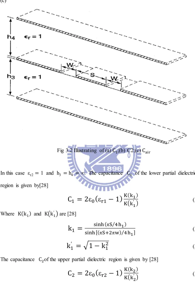
Fig 3.2 Illustrating of (a) C1;(b) C2;(c) Cair... 16
Fig 3.3 (a) the size of the main structure (b) the current path of the main structure 20 Fig 3.4 Reflection coefficient of the main structure ... 21
Fig 3.5(a) the current distribution at 780MHz (b) the current distribution at 2820MHz ... 21
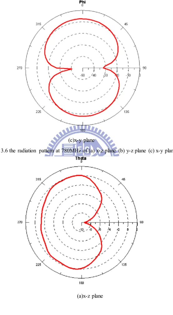
Fig 3.6 the radiation pattern at 780MHz of (a) x-z plane (b) y-z plane (c) x-y plane ... 23
Fig 3.7 the radiation pattern at 2820MHz of(a) x-z plane (b) y-z plane (c) x-y plane ... 24
Fig 3.8 the configuration of Lh, Wh and POSh ... 26
Fig 3.9 the reflection coefficient of different position ... 27
Fig 3.10 the peak gain value of different positionat 2.8GHz ... 27
Fig 3.11 the reflection coefficient of different length ... 28
Fig 3.12 the peak gain value of different length at 2.8GHz... 28
Fig 3.13 the reflection coefficient of different width... 29
Fig 3.14 the Peak gain value of different width at 2.8GHz ... 29
Fig 3.15 the configuration of SIZEs and POSs... 31
Fig 3.16 the reflection coefficient of different position ... 32
Fig 3.17 the peak gain value of different position at 2.58GHz... 32
Fig 3.18 the reflection coefficient of different size... 33
VI
Fig 3.20 the configuration of Lg, Wg, POSg ... 35
Fig 3.21 the reflection coefficient with different position ... 36
Fig 3.22 the peak gain value with different position at 2.6GHz ... 36
Fig 3.23 the reflection coefficient with different length ... 37
Fig 3.24 the peak gain value with different length at 2.6GHz ... 37
Fig 3.25 the reflection coefficient with different width ... 38
Fig 3.26 the peak gain value with different width at 2.6GHz... 38
Fig 3.27 the top view of the fabricated antenna... 40
Fig 3.28 the reflection coefficient of the measurement and the simulation... 40
Fig 3.29(a) the current distribution at 775MHz (b) the current distribution at 2520 MHz ... 41
Fig 3.30 the radiation pattern at 775 MHz of (a) x-z plane (b) y-z plane (c) x-y plane ... 42
Fig 3.31 the radiation pattern at 2570MHz of (a) x-z plane (b) y-z plane (c) x-y plane... 44
Fig 4.1 Geometry of microstrip line ... 47
Fig 4.2 Electric and magnetic field lines of microstrip line ... 47
Fig 4.3 (a) the size of the main structure (b) the current path of the main structure . 50 Fig 4.4 Reflection coefficient of the main structure ... 51
Fig 4.5 the current distribution at 780 MHz ... 51
Fig 4.6 the radiation pattern at 780MHz of (a) x-z plane (b) y-z plane (c) x-y plane ... 53
Fig 4.7 the configuration of Lh,Whr and Whl ... 55
Fig 4.8 the reflection coefficient of different width of the slot on the left side ... 56
Fig 4.9 the peak gain value of different width of the slot on the left side at 2.16GHz ... 56
Fig 4.10 the reflection coefficient of different width of the slot on the right side.... 57
Fig 4.11 the peak gain value of different width of the slot on the right side at 2.16GHz ... 57
Fig 4.12 the reflection coefficient of different length of the slot... 58
Fig 4.13 the configuration of Lhw and Whw ... 60
Fig 4.14 the reflection coefficient of different width... 60
Fig 4.15 the reflection coefficient of different length... 61
Fig 4.16 the peak gain value of different length at 2.36GHz... 61
Fig 4.17 the configuration of (a) L1 and W1 (b) L2 and W2 (c) L3 and W3 ... 63
Fig 4.18 the reflection coefficient of different L1 ... 64
Fig 4.19 the reflection coefficient of different W1... 64
VII
Fig 4.21 the reflection coefficient of different W2... 65
Fig 4.22 the reflection coefficient of different L3 ... 66
Fig 4.23 the reflection coefficient of different W3... 66
Fig 4.24 the configuration of lgnd ... 67
Fig 4.25 the reflection coefficient with different Lgnd... 68
Fig 4.26 the radiation pattern at 780MHz on the (a) x-z plane (b) x-y plane (c) y-z plane... 69
Fig 4.27 the radiation pattern at 1980MHz on the (a) x-z plane (b) x-y plane (c) y-z plane... 71
Fig 4.28 the radiation pattern at 2460MHz on the (a) x-z plane (b) x-y plane (c) y-z plane... 72
Fig 4.29 (a) the top view (b) the back view of the fabricated antenna ... 74
Fig 4.30 the reflection coefficient of the measurement and the simulation... 75
Fig 4.31 the current distribution at (a) 775MHz (b) 2020MHz (c) 2490MHz ... 76
Fig 4.32 the radiation pattern at 775MHz of (a) x-z plane (b) y-z plane (c) x-y plane ... 77
Fig 4.33 the radiation pattern at 2020MHz of (a) x-y plane (b) y-z plane (c) x-y plane... 79
Fig 4.34 the radiation pattern at 2420MHz of (a) x-z plane (b) y-z plane (c) x-y plane... 80
Fig 5.1 The Dual band antenna support part of LTE specification ... 82
Fig 5.2 A electrically small meander antenna support LTE 700 ... 82
VIII
LIST OF TABLES
Table3.1 the designed value of the small dual band antenna………39 Table4.1 the designed value of the small triple band antenna………73 Table5.1 the comparison between the proposal antennas and antennas on the papers…………83
1
Chapter 1 Introduction
1.1. Motivation
In recent years, Long Term Evolution(LTE)[1, 2] becomes a popular mobile network technology after GSM(the second generation mobile networks) and UMTS( the third generation mobile networks). It's a project of the 3rd Generation Partnership Project and a set of enhancements to the Universal Mobile Telecommunications System(UMTS).
LTE will be internet protocol(IP) based and will provide broader band , high transmission rate and reduce the wireless network delay. It will have theoretical peak data rates for downlink of at least 100 Mbps, an uplink of at least 50 Mbps and supporting scalable carrier bandwidths, from 1.4 MHz to 20 MHz.
There are two operating modes of the LTE system. One is based on time division duplexing (TDD) and another is in frequency division duplexing (FDD). FDD using the paired spectrum is anticipated to form the migration path for the current 3G services being used . TDD using unpaired spectrum is providing the evolution or upgrade path for TD-SCDMA.
In application, the LTE system can support the frequency bands of the pervious applications and so far, there are 43 operating bands. The bands are below 1GHz in this paper, we call the lower frequency band. The frequency start from 698MHz to 960MHz, include Band5, Band6, Band8 and Band12 to Band20. In application, these Bands are supported SMH blocks A/B/C/D ,Cellular 850, UMTS 800, UMTS850, GSM, UMTS 900, EGSM900 and EU’s Digital Dividend 800MHz . More than 1GHz but below 2GHz, there are two frequency bands. One start from 1427MHz to 1660MHz, include Band 11,Band 21 and Band 22 in LTE operating bands, but right now, there is just one application called PDC in japan. Another
2
one provide Band 1 to Band 4, Band10, Band 33 to Band 37and Band39. The frequency start from 1710MHz to 2170MHz. The applications include UMTS IMT2100, PCS 1900, DCS 1800, AWS, UMTS 1700, IMT2000. In this paper, this region will be called the middle frequency band. More than 2GHz and below 3GHz, there is one frequency band start from 2300MHz to 2690MHz and provide the LTE operating bands like Band7, Band 38,Band 40 and Band 41. The applications in this region are IMT-E and IMT 2000. We call the higher frequency band in this paper. There is still one frequency band more than 3GHz. Start from 3400MHz to 3800MHz , but right now, there are not supporting any applications. So in this paper, we don’t discuss that region part. But in the future, there will be applications supporting in this region, so it will be discuss in the future work section.
For the LTE antenna, the design for the lower frequency band poses some design challenges in the antenna portion of the mobile terminal due to size limitations. If using the regular antenna designs for each mobile terminals , the size of the antennas will not fit in with the small size of the applications.
3
1.2. Organization
In Chapter1, we will introduce this dissertation at beginning and describes the motivation.
In Chapter2, we will review the papers with multi-band and miniaturized antenna design in recent year.
In Chapter3, we will present the CPW feed dual band antenna for LTE frequency band. Firstly, we create the main structure to verify the lower frequency band(698MHz to 960MHz). For the higher frequency band and the peak gain , we perform the additional current paths and the slot on the ground. At last , we will show the results of this design
In Chapter 4, we will demonstrate the microstrip line feed triple band antenna for LTE frequency band. As same as in the chapter3, we create the main structure to verify the frequency band below l GHZ and using the slot-on-the-ground structure and additional current stubs to match the higher frequency band. Then, we use another additional stubs to separate the higher band to two frequency bands. After that, we discuss the ground size effect for the proposal antenna. At last , we will show the results of this design.
In Chapter 5, we will compare the volume and numbers of the supporting frequency bands with LTE system between the proposal antennas and the antennas on the papers.
The last, Chapter6, we will give the summary and the conclusion of all and the future study.
4
Chapter 2 Theories of the Antenna Structure
Design
In recent year, the miniaturizing and supporting many applications will be more and more important in the antenna design. So in this chapter, we will discuss the methods for miniaturized and multi-band antenna . In the first section, we will focus on the multi-band antenna, and discuss how to create the multi-band from the main structure, the ground plane and the substrate. The second section, we will focus on how to miniaturize the antenna, as same as the first section, we will discuss from the main structure and the ground plane.
2.1. The antenna design for the multi-band antenna
For the multiband antenna , There are several ways to achieve the aim.
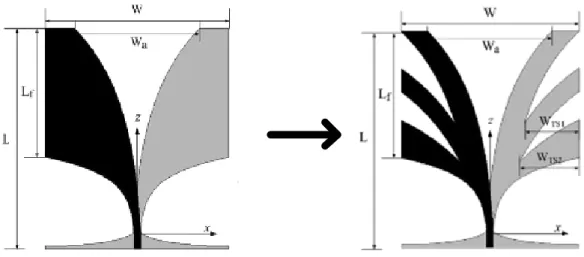
1. Increase the current path on the main structure [3-8]. The multi band means that there are many current paths exciting many different frequency bands. That’s the direction way to achieve the multi bands. Design the multi stubs are not only creating the multi band but also matching the wider band. Figure2.1[5] and Figure 2.2[7] shows the design for the multi-band. Different stubs are supporting different frequency band. The cost is the antenna gain decreasing by the current distribution of additional current paths canceling each other.
Another way to increase the frequency band and the higher bandwidth without coupling and adding stubs is limiting the shape of the main structure like Figure 2.3[8]. The transverse width of the main structure along the longitudinal direction should be wide at the beginning and then become narrower at the end.
5
Fig 2.1Multi-Band Internal Monopole Antenna
6
Fig 2.3Multi-band modified fork-shaped microstrip monopole antenna
2. Increase the frequency bands by using the additional stub on the back side of the antenna [9-11]. The difference from the previous point is the location of additional stubs don’t on the main structure, on the back side of the main structure. The antenna in Figure 2.4[10] is through the couple method , create the additional current path to match the frequency band we want. Figure 2.5[11] using stubs on the back side to create the lower frequency band and matching the higher frequency band with the main structure. The cost is the same as the first point, the antenna gain may decrease by cancel the current distribution..
7
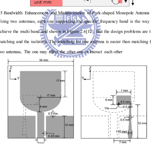
Fig 2.5 Bandwidth Enhancement and Miniaturization of Fork-shaped Monopole Antenna 3. Using two antennas, each one supporting the specific frequency band is the way to
achieve the multi band and shown in Figure 2.6[12]. But the design problems are the matching and the isolation. The matching for one antenna is easier than matching for two antennas, The one may affect the other one or interact each other
8
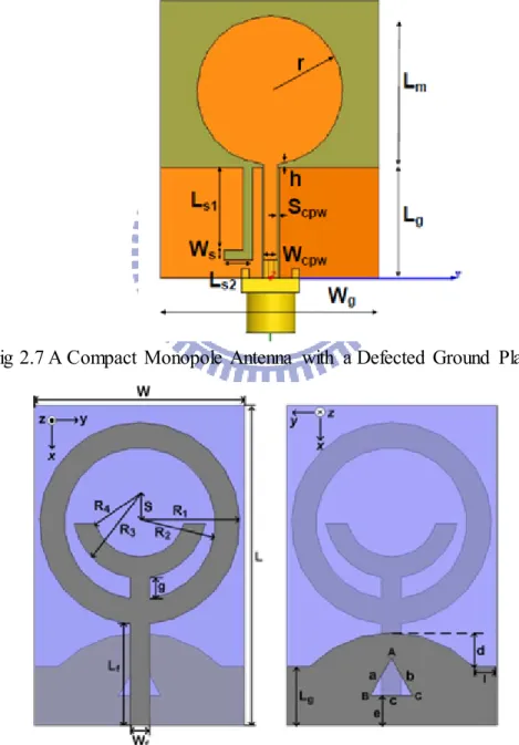
4. Using above antenna designing may achieve the multi-band. But most of situations are the reflection coefficient in the frequency band we want would not lower enough. Without changing the main structures, we will focus on the terminal of the antenna. The variation of the ground is one of the method to result the matching on the terminal[13-16].. Figure 2.7[14] shows how matching the reflection coefficient by using the slot on the ground for the CPW structure. The location , width and length of the slot are sensitive for the terminal matching. Figure2.8[15] shows using the same way matching for the microstrip line structure.
Fig 2.7 A Compact Monopole Antenna with a Defected Ground Plane
Fig 2.8 Miniaturized Triple Band Antenna With a Defected Ground Plane
9
In this section, we will review the effective dielectric constant and characteristic impedance with finite thickness by using mapping Techniques.
10
2.2. The antenna design for the miniaturized antenna
The miniaturized antenna means using some technique to support the frequency band which is lower than regular supporting. And there are several ways to achieve the aim.
1 .Increase the current path[17-22] from the original size of the antenna. If we want the lower frequency band. The current path should longer than the original one. The actual way is using the meander line or slots on the main structure to increase the current path. In Figure 2.9[17], the shape of the main structure is from the rectangle and design for the miniaturization. Figure 2.10[20] shows the method by using the slot on the main structure to match the lower frequency band.
.
11
Fig 2.10A Miniaturized Antipodal Vivaldi Antenna
3. We also can use the matching network to match the lower frequency band. The antenna can be shown as the open end network, if we use another network to match. The reflection coefficient will match the frequency band we want. Figure 2.11[23] showing the wheeler matching network is in front of the CPW feeding line with RO3010 to be a substructure.
Fig 2.11A Miniaturized Multiband Monopole Antenna Using a Double-Tuned Wheeler Matching Network
12
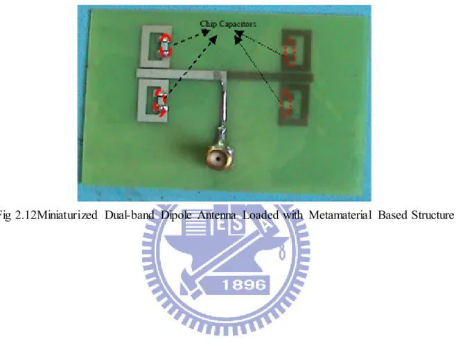
4. Another way to miniaturize the antenna is using the metamaterial to shorten the electric length. The metamaterial also can be as an LC resonant circuit with the main structure. The operating frequency with the metamaterial can shift to the lower frequency .in Figure 2.12[24]. The resonant circuit is determined by the loop inductance and the gap capacitor.
13
Chapter 3 The Small Dual Band Antenna for the
LTE System
We already introduce the LTE system and the frequency bands in Chapter1. In this antenna design, we will focus on the whole lower frequency band which start from 698 MHz to 960 MHz and the whole higher frequency band which start from 2300MHz to 2690MHz. Band 5 to Band 8, Band 12 to Band 20, Band 38, Band 40 and Band 41 of the LTE operating bands are supported. Because the lower frequency band need the longer current path, the longer current path means the bigger antenna size. In section 3.1, we first review the basic theory of coplanar waveguide structure. Then, we consider that and will be discussed in Section 3.2. After that, we improve the structure of the Section 3.2 to verify the higher frequency band and the antenna gain in rest of the sections.
3.1. The Basic Theory of Coplanar Waveguide Structure
3.1.1. Introduction
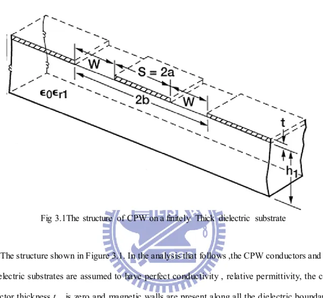
The coplanar waveguide[25](CPW) proposed by C. P. Wen in 1969 consisted of a dielectric substrate with conductors on the top surface[26]. The conductors formed a center strip separated by a narrow gap from two ground planes on either side. The dimensions of the center strip ,the gap, the thickness and permittivity of the dielectric substrate determined the effective dielectric constant (ε ),characteristic impedance (Z ) and the attenuation (α) of the line.
In this section, we will review the effective dielectric constant and characteristic impedance with finite thickness by using mapping Techniques.
14
3.1.2. Conventional Coplanar Waveguide on a Dielectric Substrate of Finite
Thickness
Fig 3.1The structure of CPW on a finitely Thick dielectric substrate
The structure shown in Figure 3.1. In the analysis that follows ,the CPW conductors and the dielectric substrates are assumed to have perfect conductivity , relative permittivity, the con- ductor thickness t is zero and magnetic walls are present along all the dielectric boundaries including the CPW slots. Hence the structure is considered to be loss less. Further the dielectric substrate materials are considered to be isotropic.
The assumptions made are that The CPW is then divided into several partial regions and the electric field is assumed to exist only in that partial region. In this manner the capacitance of each partial region is determined separately. The total capacitance is then the sum of the partial capacitances[27]. Expressions for the partial capacitances of the sandwiched CPW will be derived first and later extended to the case of CPW on a double-layer dielectric.
The total capacitance C of the sandwiched CPW is the sum of the partial capacitances C , C and C shown in Figure3.2
15
C
= C + C + C
(3.1.1) Where C and C are the partial capacitance of the CPW with only the lower and the upper dielectric layers ,respectively. Further C is the partial capacitance of the CPW in the absence of all the dielectric layers.(a)
16 (c)
Fig 3.2 Illustrating of (a) C ;(b) C2;(c) C
In this case εr2= 1 and h3 = h4 = ∞. The capacitance C of the lower partial dielectric region is given by[28]
C = 2ε (ε
− 1)
( ′ ) (3.1.2) Where K(k ) and K k′ are [28]k =
(π ⁄ )[(π π )⁄ ] (3.1.3)
k
′=
1 − k
(3.1.4) The capacitance C of the upper partial dielectric region is given by [28]
C = 2ε (ε
− 1)
( ′ )(3.1.5)
17
k =
(π ⁄ ) [(π π )⁄ ](3.1.6)
k
′=
1 − k
(3.1.7) when εr2= 1, we haveC
2= 0
(3.1.8)The capacitance C is given by [28]
C
= 2ε
( ′ )+ 2ε
( ′ )(3.1.9) where
k =
(π ⁄ ) [(π π )⁄ ](31.10)
k =
(π ⁄ ) [(π π )⁄ ](3.1.11)
k
′=
1 − k
(3.1.12)k
′=
1 − k
(3.1.13) when h3 = h4 = ∞ we havek
3= k
4= k
0=
S S 2W (3.1.14) andC
air= 4ε
0 K(k0) K k0′(3.1.15) Eq.(3.1.1) gives
C
= 2ε (ε
+ 1)
( ′ ) (3.1.16) Under quasi-static approximation ε is defined as[28]ε
=
(3.1.17) Further ν and Z are defined as [28]18
ν
=
ε (3.1.18)Z =
ν=
1 cCair εeff=
30π εeff K k0′ K(k0) (3.1.19)19
3.2. The Main Structure of The Proposed Antenna
To verify the lower frequency band , there are three things to be considered: 1.The center frequency of the lower band is 800MHz. For the monopole structure ,the electric length is λ/4 , Therefore the length(L0.8) at 800 MHz is
L
.=
. ×
= 93.75mm
(3.2.1)The current path of the antenna design must greater than L0.8 .
2.The bandwidth of the lower band is 200MHz(25%), this is such a problem for the low frequency. The antenna as the mender line structure may not be considered. The reason is because there are too many corners in the mender line structure, and it cause the antenna to be the narrow band antenna.
3. In the antenna design, the miniaturization has enable the wider range of applications, so the volume of the antenna cant not be too large.
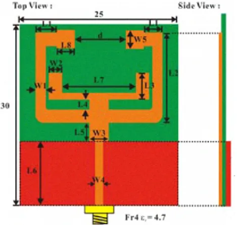
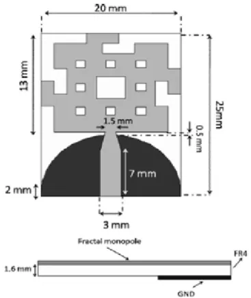
The above three considerations are the standard of what we design for. The main structure is inspiration of [30, 31] and shown in Figure 3.3(a). We use CPW feed and FR-4 to be the substrate. The thickness of the substrate is 0.8mm.
The length of the main structure is designed for the lower frequency band and shown in Figure 3.3(b). The total length is 113.2mm and longer than L0.8, so we except the 698MHz to
960 MHz frequency band will be matched and verified by the reflection coefficient shown in Figure 3.4. The lower band start from 710MHz to 920MHz and the bandwidth is 310MHz. We can also confirm by the Figure 3.5(a), the current flew goes through the whole main structure. There is another frequency band close to the spec of the LTE system but we didn’t except in the main structure design. The band start from 2620MHz to 2980MHz and the bandwidth is 370MHz. We can analysis the current path from the figure 3.5(b) and the main current just go around the part of the main structure.
20
monopole pattern and the omni-directional pattern on the x-z plane. At 2820MHa, the radiation pattern is shown in Figure 3.7(a) to Figure 3.7(c). we can see the x- z plane is not the omni-directional pattern. That is because the current flew at the higher frequency band just go around the lower left corner of the main structure, the pattern is on the -x direction. Consider that the peak gain is less than one, that will be discussed in the section 3.5.
The ground size is restricted by the antenna size and the main structure. This is because when we further decrease the ground size, the performance of this antenna will suffer a dramatic degrade , The ground size of this antenna is considered to be appropriate.
The total volume of the proposed antenna(Vola)(include the ground plane) is
Vol = 54mm × 26.6mm × 0.8 mm
= 1149.12mm
(3.2.2) It is a kind of small antenna for the operating frequency below 1GHz.(a) (b)
Fig 3.3 (a) the size of the main structure (b) the current path of the main structure
X
Y
21 0 .5 1 1.5 2 2.5 3 Frequency(GH z) -40 -30 -20 -10 0 S p a ra m e te r( d B )
Fig 3.4 Reflection coefficient of the main structure
(a) (b)
Fig 3.5(a) the current distribution at 780MHz (b) the current distribution at 2820MHz
22 0 45 90 135 180 225 270 315 Theta -15 -13 -11 -9 -7 (a)x-z plane (b)y-z plane
23 (c)x-y plane
Fig 3.6 the radiation pattern at 780MHz of (a) x-z plane (b) y-z plane (c) x-y plane
24
(b)y-z plane
(c)x-y plane
25
3.3. Shift and Increase the Bandwidth of the Higher Frequency
In this section ,we will create another path on the main structure to shift and increase the bandwidth of the higher frequency. .At 2.4GHz, the electric length of the monopole would be:
L
.=
. ×
= 31.25(mm)
( 3.2.1)If we want to create another path to control the frequency band at 2.4GHz, this additional current path should be close to
L
..
The position and the length of the stub have to handle this part. Although it would be better that the current path more and more close toL
. , the variation of the antenna gain is also concerned. We use the antenna peak gain at 2.8GHz to be the reference. Notice that the width of the stub may affect the performance, too . So there are three parameters:the position of the path( POSh ) , the length of the path(Lh) andthe width of the path(Wh) would be discussed and shown in Figure 3.8.
Figure 3.9 shows that when the position near to the terminal, the bandwidth would increase from 400MHz to 580MHz, but the antenna gain would be decreased except POSh = 23mm
and shown in Figure 3.10.
The Figure 3.11 and the Fiugre3.12 show how the variation of the length of the stub would result the reflection coefficient and the antenna gain . When the length is longer ,the current path is more and more close to the length at 2.4GHz, but the antenna peak gain decrease. For the balance of the reflection coefficient and the antenna gain, Lh = 16mm would be a better
choice.
The Figure 3.13 and the Figure 3.14 show the variation of the width of the stub. The reflection coefficient would not be affected by changing the width, but the antenna gain would. When Wh = 2mm ,the antenna gain value be better than others.
According to above discussion, the parameters of the additional stub would be POSh =
26
2.54GHz and the bandwidth increase from 370MHz to 440MHz .The lower frequency band is the same as the previous section, 710MHz to 920MHz.
27 With Lh = 16mm, Wh = 2mm 0.5 1 1.5 2 2.5 3 Frequency(GHz) -50 -40 -30 -20 -10 0 S p a ra m e te r( d B ) POSh = 21mm POSh = 22mm POSh = 23mm POSh = 24mm POSh = 25mm
Fig 3.9 the reflection coefficient of different position
21 22 23 24 25 POSh(mm) -0.4 0 0.4 0.8 1.2 P e a k G a in (d B )
Fig 3.10 the peak gain value of different position at 2.8GHz
28 With POSh = 23mm, Wh = 2mm 0.5 1 1.5 2 2.5 3 Frequency(GHz) -80 -60 -40 -20 0 S p a ra m e te r( d B ) Lh = 15mm Lh = 16mm Lh = 17mm
Fig 3.11 the reflection coefficient of different length
15 16 17 Lh(mm) -0.4 0 0.4 0.8 1.2 1.6 P e a k G a in (d B )
29 With Lh = 16mm, POSh = 23mm 0.5 1 1.5 2 2.5 3 Frequency(GHz) -40 -30 -20 -10 0 S p a ra m e te r( d B ) Wh = 1mm Wh = 2mm Wh = 3mm
Fig 3.13 the reflection coefficient of different width
1 2 3 Wh(mm) 0 0.4 0.8 1.2 P e a k G a in (d B )
30
3.4. Shift the Bandwidth of the Higher Band by Using a Slot on the Ground
For the pervious section , we used the additional stub to shift and increase the bandwidth of the higher frequency and it's work. But the bandwidth is still not in the region we want. This section will use the slot on the ground to solve this problem.
In order to create another little lower frequency resonances in the response of the monopole , a slot was cut out of the antenna ground plane shown in Figure3.15. An square slot was chosen in order to achieve a effective slot length without having to change the main structure of the antenna.
For this asymmetric structure of the antenna, the slot on the right side of the ground doesn't result the reflection coefficient or the antenna gain. The slot on the left side of the ground does. Different positions(POSS) and sizes(SIZES) would affect the S parameter and the antenna
gain .
The
Figure 3.16 and the Figure 3.17 show when the slotfar from the main structure, the reflection coefficient will be better, but the antenna gain will be worse. At POSS = 12mm, thebandwidth at higher frequency start from 2.42GHz and not meet the needs of the LTE specification. So we choose POSS = 10mm.
The
Figure3.18 and the Figure 3.19 show the variation of the reflection coefficient and the antenna gain with the slot size changing. When the slot is larger, the effect of the reflection coefficient will be increase and the antenna peak gain will decrease. SIZES = 3mm x 3mmwould be a better choice.
In the end , we choose POSS = 10mm and SIZES = 3mm x 3mm to design the slot. The
31
32 With SIZES = 3mm x 3mm 0.5 1 1.5 2 2.5 3 Frequency(GHz) -50 -40 -30 -20 -10 0 S p a ra m e te r( d B ) POSs= 6mm POSs= 8mm POSs= 10mm POSs= 12mm
Fig 3.16 the reflection coefficient of different position
6 8 10 12 POSs(mm) -1.2 -0.8 -0.4 0 0.4 0.8 P e a k G a in (d B )
33 With POSS = 10mm 0.5 1 1.5 2 2.5 3 Frequency(GHz) -50 -40 -30 -20 -10 0 S p a ra m e te r( d B ) SIZEs = 2mm x 2mm SIZEs = 3mm x 3mm SIZEs = 4mm x 4mm
Fig 3.18 the reflection coefficient of different size
2 3 4 SIZEs(mm x mm) 0 0.1 0.2 0.3 P e a k G a in (d B )
34
3.5. Improve the Antenna Gain of the Higher Frequency Band
When using additional stub and the slot-on-the-ground structure, the bandwidth at 2300MHz to 2700MHz will match the specification. But the peak gain turn down to 0.2dB and it should more than one .In this section, we will increase the antenna gain by adding the stub on the main structure but would not result the S parameter at the frequency we want. We use the upper half of the space to increase the value. The Figure 3.17 shows the position of additional stub. As same as the section 3.3. There are also three parameters to affect the performance. The position of the stub (POSg), the length of the stub (Lg) and the width of the
stub(Wg).
Figure 3.20 and Figure 3.21 show the difference of the reflection coefficient with different positions. The variation of the reflection coefficient doesn't rapid change. But the antenna gain at 2.6GHz would be better with POSg= 35mm.
Figure3.22, Figure 3.23, Figure 3.24 and Figure 3.25 show the variation of the reflection coefficient and the antenna peak gain by different length and width. Because we use the upper half of the space of the antenna, The reflection coefficient does not change rapidly. We finally choose POSg= 35mm ,Lg = 6mm , Wg = 4mm for designed values . The bandwidth at the
lower frequency start form 680MHz to 880MHz..For the specification of the LTE system, the antenna gain below 1GHz must greater than -10dB. The peak gain at 775MHz is -7.8dB and can be used. The higher band is form2300MHz to 2700MHz.and the antenna peak gain at 2.6GHz is 1.5 dB.
35
36 With Lg = 6mm , Wg = 4mm 0.5 1 1.5 2 2.5 3 Frequency(GHz) -50 -40 -30 -20 -10 0 S p a ra m e te r( d B ) POSg = 34mm POSg = 35mm POSg = 36mm POSg = 37mm
Fig 3.21 the reflection coefficient with different position
34 35 36 37 POSg(mm) 0.8 1 1.2 1.4 1.6 P e a k G a in (d B )
37 With POSg = 35mm , Wg = 4mm 0.5 1 1.5 2 2.5 3 Frequency(GHz) -40 -30 -20 -10 0 S p a ra m e te r( d B ) Lg = 4mm Lg = 5mm Lg = 6mm Lg = 7mm Lg = 8mm
Fig 3.23 the reflection coefficient with different length
4 5 6 7 8 Lg(mm) 1 1.2 1.4 1.6 P e a k G a in (d B )
38 With Lg = 6mm , POSg = 35mm 0.5 1 1.5 2 2.5 3 Frequency(GHz) -80 -60 -40 -20 0 S p a ra m e te r( d B ) Wg = 2mm Wg = 4mm Wg = 6mm
Fig 3.25 the reflection coefficient with different width
2 3 4 5 6 Wg(mm) 1.2 1.3 1.4 1.5 1.6 P e a k G a in (d B )
39
3.6. The Comparison Between the measurement and The Simulation
According to the above sections, we sort out the parameters we use to the Table 3.1. The fabricated antenna is shown in Fig 3.27, The volume of the proposed antenna is just 1149.12mm3.In the commercial application, VSWR 3:1 is the regular specification. With the
reflection coefficient, the frequency band for designing have to greater than -6dB and shown in Fig 3.28.For the measurement, the lower frequency band is from 640MHz to 960MHz and the bandwidth is 320MHz. The higher band is from 2150MHz to 2920MHz, the bandwidth is 770MHz.
Figure 3.29(a) and Figure 3.29(b) shows the current distribution at 775 MHz and 2570 MHz. We can see at the lower frequency, the main current go through the whole main structure. So the radiation pattern will be the omni-direction. At the higher frequency, the main current is just on the left side. So the radiation pattern will toward one direction.
The radiation pattern at 775MHz is the monopole pattern and the omni-direction on the x-z plane as shown in Fig 3.30(a) to Fig 3.30(c). The peak gain value is about -10dB which is just the minimum value of the specification of the LTE system. Fig 3.31(a) to Fig3.31(c) shows the radiation pattern at 2570MHz . The main radiation direction is -x direction and the peak gain is about 1.2dB . Although the value reduce 0.3dB, but still in the range of the usage.
Section 3.2 Section 3.3 Section 3.4
POSh 23mm POSs 10mm POSg 35mm
Lh 16mm SIZEs 3mm x 3mm Lg 6mm
Wh 2mm Wg 4mm
40
Fig 3.27 the top view of the fabricated antenna
0.5 1 1.5 2 2.5 3 Frequency(GHz) -30 -20 -10 0 S p a ra m e te r( d B ) Measurement Simulation
41
(a) (b)
Fig 3.29(a) the current distribution at 775MHz (b) the current distribution at 2520 MHz
0
45
90
135
180
225
270
315
Theta
-40
-30
-20
-10
0
measurement
simulation
(a) x-z plane x y z42 0 45 90 135 180 225 270 315 Theta -40 -30 -20 -10 0 measurement simulation (b) y-z plane 0 45 90 135 180 225 270 315 Phi -50 -40 -30 -20 -10 0 measurement simulation (c)x-y plane
Fig 3.30 the radiation pattern at 775 MHz of (a) x-z plane (b) y-z plane (c) x-y plane
x y
43
0
45
90
135
180
225
270
315
Theta
-10 -8 -6 -4 -2 0
2
measurement
simulation
(a) x-z plane 0 45 90 135 180 225 270 315 Theta -10 -8 -6 -4 -2 0 2 measurement simulation (b) y-z palne x y z44
0
45
90
135
180
225
270
315
Phi
-15 -12 -9
-6
-3
0
measurement
simulation
(c)x-y planeFig 3.31 the radiation pattern at 2570MHz of (a) x-z plane (b) y-z plane (c) x-y plane
x y
45
Chapter 4 The Small Triple Band Antenna for the
LTE System
Except the operation frequency band we design in pervious Chapter(698MHz to 960MHz
and 2300 MHz to 2690 MHz), we want to enable the more wider range of applications and the size of the antenna doesn't change a lot. In this chapter, we increase the middle band start from 1710MHz to 2170MHz.. The reason we don’t include the bands 1427MHz to 1660MHz is because the application in this region just one. In the first section, we still review the basic theory of Microstrip line first. Then in section 4.2, we consider the lower frequency band (698MHz to 950MHz) to be the main structure of the proposed antenna. After that, we create the higher frequency band by using the slot on the ground structure and the additional stub on the main structure to improve the bandwidth and the antenna gain. At last, we use the notch concept to separate the higher frequency band to the dual band to achieve the triple frequency band.
4.1. The Basic Theory of Microstrip Line Structure
4.1.1. Introduction
Microstrip line[32] is one of the most popular types of planar transmission lines , because it can be fabricated by photolithographic processes and is easily integrated with other passive and active microwave devices. The geometry of a microstrip line is shown in Figure 4.1. A conductor of width W is printed on a thin, grounded dielectric substrate of thickness d and relative permittivity ϵ . a sketch of the field lines is shown in Figure 4.2.
If the dielectric constant is equal to the dielectric constant as a free space , we could think of the line as a two-wire line consisting of two flat strip conductors of width W, separated by a distance 2d (the ground plane can be removed via image theory). In this case we would have
46
a simple TEM transmission line, with ν = c and β = k .
The presence of the dielectric, and particularly the fact that the dielectric does not fill the air region above the strip (y > d), complicates the behavior and analysis of microstrip line. Unlike stripline, where all the fields are contained within a homogeneous dielectric region, microstrip has some (usually most) of its field lines in the dielectric region, concentrated between the strip conductor and the ground plane, and some fraction in the air region above the substrate. For this reason the microstrip line cannot support a pure TEM wave, since the phase velocity of TEM fields in the dielectric region would be c/√ϵ , but the phase velocity of TEM fields in the air region would be c. Thus, a phase match at the dielectric-air interface would be impossible to attain for a TEM-type wave.
In actuality, the exact fields of a microstrip line constitute a hybrid TM-TE wave, and
require more advanced analysis techniques than we are prepared to deal with here. In most practical applications, however, the dielectric substrate is electrically very thin (d << ), and so the fields are quasi- TEM. In other words , the fields are essentially the same as those of the static case. Thus, good approximations for the phase velocity, propagation constant, and characteristic impedance can be obtained from static or quasi-static solutions. Then the phase velocity and propagation constant can be expressed as
ν
=
(4.1.1)
β
= k
ϵ
(4.1.2) where ϵ , is the effective dielectric constant of the microstrip line. Since some of the field lines are in the dielectric region and some are in air, the effective dielectric constant satisfies the relation1 < ϵ < ϵ
(4.1.3) and is dependent on the substrate thickness, d, and conductor width W. We will first present design formulas for the effective dielectric constant and characteristic impedance of micro-47
strip line; these results are curve-fit approximations to rigorous quasi-static solutions[33, 34].
Fig 4.1 Geometry of microstrip line
Fig 4.2 Electric and magnetic field lines of microstrip line
4.1.2. Formulas for Effective Dielectric Constant ,Characteristic
impedance, and Attenuation
The effective dielectric constant of a microstrip line is given approximately by
ϵ =
+
(4.1.4)The effective dielectric constant can be interpreted as the dielectric constant of a homo- generous medium that replaces the air and dielectric regions of the microstrip. The phase velocity and propagation constant are then given by Eq.(4.1.1) and (4.1.2). Given the dim- ensions of the microstrip line, the characteristic impedance can be calculated as
48
Z =
ln
+
π . . .(4.1.5) For a given characteristic impedance Z and dielectric constant ϵ ,the W d ratio can be found as
=
πB − 1 − ln(2B − 1) +
ln B − 1 + 0.39 −
. (4.1.6) whereA =
+
0.23 +
.(4.1.7)
B =
π √(4.1.8)
Considering microstrip as a quasi-TEM line, the attenuation due to dielectric loss can be determined as
α
=
( ( ) ) δ(4.1.9) where tan
δ
is the loss tangent of the dielectric. which accounts for the fact that the fields around the microstrip line are partly in air (lossless) and partly in the dielectric. The attenuation due to conductor loss is given approximately by [33]α
=
(4.1.10) Where R = ωμ ⁄2σ is the surface resistivity of the conductor. For most microstrip sub-
strates, conductor loss is much more significant than dielectric loss; exceptions may occur with some semiconductor substrates.
for W d ≤ 2 for W d ≥ 2 for W d ≤ 1 for W d ≥ 1
49
4.2. The Main Structure of The Proposed Antenna
As same as in Chapter 3, we first consider the lower frequency band to decide the antenna size . In Chapter3, we define L0.8 to be a notation of the electric length in the monopole
antenna at 800MHz. Still, the designed length must greater than L0.8. For the wider band in
the low frequency, the number of the corners must be minimizing to avoid becoming the narrow bandwidth antenna.
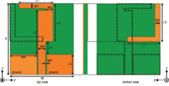
In this structure, we use microstrip line feed and FR-4 to be a substrate. The dielectric constant εr = 4.4 and the thickness of the substrate is still 0.8mm. The structure is shown in
Figure 4.3(a) and the length of the main structure is about 109mm and shown in Figure 4.3(b). From Figure 4.4, we can see that the antenna support the frequency band from 740MHz to 940MHz. The current distribution in Figure 4.5 showing the main current is around the whole antenna structure.
The radiation pattern at 780MHz still a good monopole pattern shown in Figure 4.6(a) to Figure 4.6(c) , the omni-directional pattern is on the x-z plane.
The ground size of the proposed antenna is minimized, if the length is small than 15mm, the reflection coefficient will change sensitively by the variation of the length.
Consider that the volume of the proposed antenna(VolA2) is
Vol
= 25mm × 54mm x 0.8mm
= 1080mm
(4.2.1) It smaller than the proposed antenna in pervious chapter.50
(a) (b)
Fig 4.3 (a) the size of the main structure (b) the current path of the main structure
X
Y
51 0.5 1 1.5 2 2.5 3 Frequency(GHz) -25 -20 -15 -10 -5 0 S p a ra m e te r( d B )
Fig 4.4 Reflection coefficient of the main structure
52 0 45 90 135 180 225 270 315 Theta -16 -14 -12 -10 -8
(a)x-z plane
(b)y-z plane
53 (c)x-y plane
54
4.3. Create the Bandwidth at High Frequency by Using the Slot on the
Ground Plane
From the previous section , the main structure just fit the frequency band below 1000MHz. At higher frequency, there is no bandwidth. In this section, we will create the bandwidth at higher frequency by using the slot on the ground plane as shown in Figure4.7 .
As same as the antenna we presented in Chapter3. The main structure is an asymmetric structure ,so the slot on the left side of the feeding line is more effective than the slot on the right side of the feeding line. There are three parameters that we will be discussed: the width of the slot on the left side of the feeding line(Whl), the width of the slot on the right side of the
feeding line(Whr) and the length of the slot on the ground(Lh).
Figure 4.8 and Figure 4.9 show the variation of the reflection coefficient and the antenna peak gain with different Whl .When Whl increase , the bandwidth at higher frequency will
increase , the gain will decrease except Whl = 3.5mm. Although the peak gains are small for
all valued Whl , but it still can be the basis to decide the value which is chosen. In this case, we
choose Whl = 3.5mm.
Figure 4.10 and Figure 4.11 show the variation of the reflection coefficient and the peak gain with different Whr.There is no significant change in the Figure 4.10. That's the same as
how we expect. We choose Whr = 4mm to be our design parameter. The reason not to choose
Whr = 5mm , which the peak gain higher than Whr = 4mm is because for the next section, the
performance with Whr = 4mm is better than Whr = 5mm.
The length of the slot is always the important parameter in the slot-on-the-ground structure. The variation of the reflection coefficient with different length is shown in Figure 4.12. The slot is more longer, the bandwidth of the high frequency will shift to lower. In this case, we choose Lh = 10mm because this frequency band is more closing to what we design. The
55
56 With Whr = 4mm ,Lh = 10mm 0.5 1 1.5 2 2.5 3 Frequency(GHz) -25 -20 -15 -10 -5 0 S p a ra m e te r( d B ) Whl= 2.5mm Whl= 3mm Whl= 3.5mm Whl= 4mm
Fig 4.8 the reflection coefficient of different width of the slot on the left side
2.5 3 3.5 4 Whl(mm) -1.32 -1.28 -1.24 -1.2 -1.16 -1.12 P e a k G a in (d B )
57 With Whl = 3.5mm ,Lh = 10mm 0.5 1 1.5 2 2.5 3 Frequency(GHz) -25 -20 -15 -10 -5 0 S p a ra m e te r( d B ) Whr = 3mm Whr = 4mm Whr = 5mm
Fig 4.10 the reflection coefficient of different width of the slot on the right side
3 4 5 Whr(mm) -1.36 -1.32 -1.28 -1.24 -1.2 P e a k G a in ( d B )
58 With Whr = 4mm, Whl = 3.5mm 0.5 1 1.5 2 2.5 3 Frequency(GHz) -25 -20 -15 -10 -5 0 S p a ra m e te r( d B ) Lh = 6mm Lh = 8mm Lh = 10mm Lh = 12mm
59
4.4. Increase the Bandwidth at Higher Frequency
In the previous sections, we already create the high frequency band and shift to the frequency we want. In this section, we want to increase the bandwidth to match the LTE specification (1710MHz~ 2170MHz, 2300MHz~ 2700MHz). The technique is creating another stub as same as we used in Chapetr3.
Because we want to separate the higher band to the dual band, the operating frequency should start below the frequency we want, So we choose the frequency at 2GHz be a reference.
λ =
×
= 37.5mm
(4.4.1)The location of the additional stub base on the length of
λ
and shown in Figure 4.13. Figure 4.14 shows the reflection coefficient with different width of additional stub(whw),the variation is very small. But what we choose Whw = 2mm is because when we use another
values, there are not the proper values for the next antenna design.
Figure 4.15 and Figure 4.16 show the reflection coefficient and the peak gain with different Lhw. With different Lhw, just result the bandwidth at the higher frequency band and the peak
gain. We choose Lhw = 23mm for designing and the frequency band at higher frequency is
from 2.08GHz to 2.7GHz.
60
Fig 4.13 the configuration of Lhw and Whw With Lhw = 23mm 0.5 1 1.5 2 2.5 3 Frequency(GH z) -25 -20 -15 -10 -5 0 S p a ra m e te r( d B ) Whw = 1mm Whw = 2mm Whw = 3mm
61 With Whw = 2mm 0.5 1 1.5 2 2.5 3 Frequency(GHz) -25 -20 -15 -10 -5 0 S p a ra m e te r( d B ) Lhw = 17mm Lhw = 20mm Lhw = 23mm
Fig 4.15 the reflection coefficient of different length
17 20 23 Lhw(mm) 0.8 0.9 1 1.1 1.2 1.3 P e a k G a in (d B )
62
4.5. Separate to the Dual band at Higher Frequency
In this section, we will separate this higher band to the dual band to meet the needs of LTE band ( 1710MHz to 2100MHz and 2300MHz to 2700MHz). We use additional stubs connected with the main structure to achieve this aim. The structure is shown in Figure 4.17.
The purpose by using the additional stubs is creating the notch point in the reflection coefficient .Separate one frequency band to the dual band , and still not affect the total bandwidth .The stubs are composed by three lines. There are two parameters for each line, the length and the width. Total parameters are six (L1,W1,L2,W2,L3 and W3).
The variation of changing the length and the width are showing below(Figure 4.19 to Figure 4.24).The variation of changing the length is more than changing the width. Figure 4.19 shows when L1 increase, the notch point will move to lower frequency and changing the
first bandwidth of the dual band Figure 4.20 shows when W1 increase , the notch point will
move to higher frequency and the bandwidth of these two frequency band will be changed rapidly.
The variation of the reflection coefficient with different L2 and L3 is much like the variation
of reflection coefficient with different L1 but changing smaller .With different W2 and W3 , the
changing are getting more and more smaller. We can use L1,W1 and L2 to control the notch
point and fine tuning with different W2,L3 and W3 for the LTE specification. At last, We use
L1 = 14.5mm, L2 = 4mm ,L3 = 11mm and W1 = W2 = W3 = 1mm to be the designed value.
The frequency band start from 680MHz to 880MHz ,1900MHz to 2060MHz and 2300MHz to 2760MHz. The gain values with these three frequency bands are -8.6dB, 0.278dB and 1dB, respectively.
63
(a)
(b)
(c)
64 With W1 = 1mm, L2 = 4mm, W2 = 1mm, L3 = 11mm, W3 = 1mm 0.5 1 1.5 2 2.5 3 Frequency(GHz) -40 -30 -20 -10 0 S p a ra m e te r( d B ) L1 = 13.5mm L1 = 14.5mm L1 = 15.5mm
Fig 4.18 the reflection coefficient of different L1
With L1 = 14.5mm, L2 = 4mm, W2 = 1mm, L3 = 11mm, W3 = 1mm 0.5 1 1.5 2 2.5 3 Frequency(GHz) -40 -30 -20 -10 0 S p a ra m e te r( d B ) W1 = 0.5mm W1 = 1mm W1 = 1.5mm
65 With L1 = 14.5mm W1 = 1mm , W2 = 1mm, L3 = 11mm, W3 = 1mm 0.5 1 1.5 2 2.5 3 Frequency(GHz) -50 -40 -30 -20 -10 0 S p a ra m e te r( d B ) L2 = 3mm L2 = 4mm L2 = 5mm
Fig 4.20 the reflection coefficient of different L2
With L1 = 14.5mm W1 = 1mm, L2 = 4mm, L3 = 11mm, W3 = 1mm 0.5 1 1.5 2 2.5 3 Frequency(GHz) -40 -30 -20 -10 0 S p a ra m e te r( d B ) W2 = 0.5mm W2 = 1mm W2 = 1.5mm
66 With L1 = 14.5mm W1 = 1mm, L2 = 4mm ,W2 = 1mm , W3 = 1mm 0.5 1 1.5 2 2.5 3 Frequency(GHz) -40 -30 -20 -10 0 S p a ra m e te r( d B ) L3 = 10mm L3 = 11mm L3 = 12mm
Fig 4.22 the reflection coefficient of different L3 With L1 = 14.5mm W1 = 1mm, L2 = 4mm, W2 = 1mm, L3 = 11mm 0.5 1 1.5 2 2.5 3 Frequency(GHz) -40 -30 -20 -10 0 S p a ra m e te r( d B ) W3 = 0.5mm W3 = 1mm W3 = 1.5mm
67
4.6. The comparison with different length of the ground
For the RF system , the ground will support not only the antenna but also the RF devices. The problem with the miniaturized antenna in design is how sensitive with changing the ground size. In this section, we will discuss the variation of the reflection coefficient and the radiation pattern with changing lgnd which is shown in Figure4.25. Figure 4.26 shows the reflection coefficient doesn’t change or shift by the ground size increases, still support the frequency band we want. The radiation pattern at 780MHz, 1980MHz and 2420MHz would not change by the variation of the ground size, just the antenna gain increase by increasing th size and shown in Figure 4.27 to Figure 4.29.
According to above result, the proposed triple band antenna can use in the RF system and the performance will not change by the ground of the system.
l
gnd68
Fig 4.25 the reflection coefficient with different Lgnd
0 45 90 135 180 225 270 315 Theta -20 -16 -12 -8 lgnd = 15mm lgnd = 20mm lgnd = 25mm (a)x-z plane x y z
69 0 45 90 135 180 225 270 315 Phi -40 -30 -20 -10 0 lgnd = 15mm lgnd = 20mm lgnd = 25mm (b)x-y plane 0 45 90 135 180 225 270 315 Theta -30 -25 -20 -15 -10 -5 lgnd = 15mm lgnd = 20mm lgnd = 25mm (c)y-z plane
Fig 4.26 the radiation pattern at 780MHz on the (a) x-z plane (b) x-y plane (c) y-z plane
x y
70 0 45 90 135 180 225 270 315 Theta -8 -6 -4 -2 0 2 lgnd = 15mm lgnd = 20mm lgnd = 25mm (a)x-z plane 0 45 90 135 180 225 270 315 Phi -30 -20 -10 0 10 lgnd = 15mm lgnd = 20mm lgnd = 25mm (b)x-y plane x y z
71 0 45 90 135 180 225 270 315 Theta -12 -8 -4 0 lgnd = 15mm lgnd = 20mm lgnd = 25mm (c)y-z plane
Fig 4.27 the radiation pattern at 1980MHz on the (a) x-z plane (b) x-y plane (c) y-z plane
0 45 90 135 180 225 270 315 Theta -8 - 6 -4 -2 0 2 4 Lgnd = 15mm Lgnd = 20mm Lgnd = 25mm (a)x-z plane x y z