國 立 交 通 大 學
電子物理學系
碩士論文
隱藏式選擇性閘極結構之薄膜電晶體記憶體元件研究
A Study on Wrapped-Select-Gate SONOS-type Thin
Film Transistor Memory Devices
指導教授:趙天生 博士
研 究 生:薛芳昌
隱藏式選擇性閘極結構之薄膜電晶體記憶體元件研究
A Study on Wrapped-Select-Gate SONOS-type Thin
Film Transistor Memory Devices
研 究 生 :薛芳昌 Student : Fang-Chang Hsueh
指導教授 :趙天生 博士 Advisor : Dr. Tien-Sheng Chao
國立交通大學
電子物理學系
碩士論文
A Thesis
Submitted to Department of Electrophysics
National Chiao Tung University
In Partial Fulfillment of the Requirements
for the Degree of Master of Science
In Electrophysics
June 2011
Hsinchu, Taiwan, Republic of China
中 華 民 國 一 ○ ○ 年 六 月
I
隱藏式選擇性閘極結構之薄膜電晶體記憶體元件研究
指導教授:趙天生 博士
研究生:薛芳昌
摘要
我們首先提出一種新穎的隱藏式選擇性閘極結構薄膜電晶體記憶體元件,它 的製程條件不僅簡單,也能與傳統的標準 CMOS 製程相容,特別適合嵌入式非 揮發性記憶體的應用。在本篇論文中,我們首次在薄膜電晶體記憶體元件中嘗試 更為有效的電子注入之源極端注入方式(Source-Side-Injection)來做寫入,以及能 帶到能帶穿隧產生之熱電洞(BTBTHH)的機制來作為電子抹除的操作。此外,我 們也同時驗證可消除二位元效應以及可在單一位元胞進行二位元的操作。值得注 意的是,薄膜電晶體記憶體所需較大的操作偏壓會造成較嚴重的偏壓干擾現象, 包括閘極干擾和汲極干擾。不同於分離式的電荷儲存元件,懸浮閘極結構的薄膜 電晶體記憶體在寫入以及抹除操作中,面臨了可能威脅到免於二位元效應特性的 懸浮閘極電壓耦合效應問題。 與單純由氮化矽組成的電子捕捉層和懸浮閘極結構的元件相比,在氮化矽中 加入內嵌式矽奈米晶體作為電子捕捉層的元件,經過耐久度測試後的元件,都能 夠有較佳的電子保存能力(約 6-8%的漏電改善),尤其是在高溫的電子保存性量測 中更為明顯。在耐久可靠度測試中,氮化矽元件以及在氮化矽中加入內嵌式矽奈 米晶體作為電子捕捉層的元件有嚴重的電子電洞不匹配的問題以及在氧化矽中 造成許多缺陷,這些造成元件的記憶體窗有關閉的傾向。然而對於懸浮閘極結構 的記憶體元件而言,即使寫入狀態和抹除狀態的閥值電壓都會隨著測試次數增加 而上升,仍然不會發生記憶體窗關閉的現象。II
A Study on Wrapped-Select-Gate SONOS-type Thin
Film Transistor Memory Devices
Advisor : Dr. Tien-Sheng Chao Student : Fang-Chang Hsueh
Abstract
For the first time, we proposed the novel Wrapped-Select-Gate (WSG) SONOS-type thin film transistor (TFT) memory device. The fabrication process of WSG structure memory device is not only simple but also compatible to conventional standard CMOS technology which fits for embedded non-volatile memory applications. In this thesis, we firstly apply source-side-injection (SSI) mechanism to three kinds SONOS-type thin film transistor memory and perform erase operation with Band-to-Band Tunneling Hot-Hole (BTBTHH). Furthermore, the elimination of 2nd bit effect and 2 bit per cell operation are also demonstrated in the same time. It is worth to note that higher operation voltage in TFT memory causes serious disturb phenomena including word-line disturbance and bit-line disturbance. Unlike to discrete charge trapping devices, TFT memory cell with floating gate structure have floating gate coupling concerns in every program or erase operation which may threaten the immunity to 2nd bit effect.
Compared to pure nitride trapping layer and floating gate structure, nitride with embedded silicon nanocrystals (Si-NCs) as trapping layer material always has better retention characteristics (6-8% improvement) when device already suffers 10k times P/E cycle, especially in high temperature retention test. In endurance characteristics, Nitride cell and Nitride_Dot cell suffer charge mismatch problem and generation of oxide defects which gives rise to window closure phenomenon while Floating gate cell still can maintain memory window even though both threshold voltage of program state and erase state keep on a rise.
III
誌謝
學生能夠順利完成碩士班的研究工作,首先必須感謝家人的支持,謝謝我的 母親李碧連女士為家庭付出的一切,謝謝我的哥哥薛世峰總是樹立良好的典範讓 我有明確的努力目標,謝謝和我攜手走向第六個年頭的宜螢,你們是我生命中最 重要的人,在我求學過程中遭遇許多挫折的時候,總是在我身邊不斷幫我加油打 氣,令我感到安心。感謝你們的陪伴,與你們共享成就與喜悅是我最大的進步原 動力。 在兩年碩士班生涯中,最要感謝的是我的指導老師趙天生教授,在我尚未具 有任何半導體專業知識的時候,老師提供我豐富的學習資源以及實驗環境,使我 這顆剛入門的小種子能夠迅速發芽茁壯,除了實驗上的知識,老師平日的諄諄教 誨以及日常待人處事的方法都讓我獲益匪淺,在此由衷地感謝老師。 此外,我要特別感謝王冠迪學長以及江宗育學長,在我的碩士論文以及元件 製程與量測實驗上給予我相當多的指導幫助。同時也感謝實驗室眾多學長姊的照 顧,其中包括了郭伯儀學長、呂侑倫學長、林哲緯學長、呂宜憲學長、廖家駿學 長、吳翊鴻學長、鄭子彥學長、嚴立丞學長、林玉喬學姊、李時璟學長、劉聿民 學長、穆政昌學長、林岷臻學姊以及林琬琦學姊,也謝謝與我同時期進入這大家 庭的夥伴:添舜、其儒、立盈、昱璇,有你們的陪伴讓生活充滿歡笑,最後謝謝 劭軒、柔含和明慈讓實驗室變得更加活潑。兩年的時間過得很快,在繁重的研究 工作之餘,我們也一起跑遍了南投天梯、宜蘭海景、墾丁衝浪、阿里山日出和驚 心動魄的漆彈生存遊戲,在各奔東西之際,感謝也祝福大家未來能順利通過各個 階段的考驗。 最後謝謝與我一起度過六年排球生涯的戰友們:育詮、家政、明儒、靖堯, 有你們的陪伴,我的生活一點也不孤單。即使我們選擇的工作方向不同了,但我 們所建立起的革命情感卻會更加深地烙印在心中,讓我們繼續為維持十八歲體能 的目標一同努力吧!IV
Contents
Chapter 1………...……….…1
Introduction………..………..1
1.1 Overview of memory device and its challenges ... 1
1.2 Brief Introduction of SONOS Flash Memory Device ... 2
1.3 Brief Introduction of Nanocrystal Memory Device ... 3
1.4 Brief Introduction of Thin-Film Transistor Memory ... 4
1.5 Motivation ... 5
1.6 Organization of the thesis ... 6
Chapter 2………...…...10
Device Fabrication and Experimental Setup………...…….10
2.1 Introduction ... 10
2.2 Experimental Procedure ... 10
2.3 Measurement and Equipment Setup ... 11
2.4 Operation of Program/Erase/Read ... 12
2.5 Disturbance Characteristics ... 13
Chapter 3………...23
Characteristics of WSG-SONOS-type TFT memory……...23
3.1 Introduction ... 23
3.2 Results and Discussions ... 23
3.3 Summary ... 27
Chapter 4……….. 49
V
4.1 Introduction ... 49
4.2 Results and Discussions ... 49
4.3 Summary ... 54
Chapter 5……….……….65
Conclusions……….………..……65
5.1 Conclusions ... 65 5.2 Future work ... 66References……….68
Chapter 1 ... 68 Chapter 2 ... 70 Chapter 3 ... 71 Chapter 4 ... 73VI
Figure caption
Chapter 1
Fig. 1. 1 The equivalent circuit schematic of NOR architecture. ... 7
Fig. 1. 2 The equivalent circuit schematic of NAND architecture. ... 7
Fig. 1. 3 Definition of ―1’’ and ―0‖ state in Id-Vg curve ... 8
Fig. 1. 4 Schematic of conventional SONOS-type NVM device ... 9
Fig. 1. 5 Schematic of nanocrystal memory device ... 9
Chapter 2
Fig. 2. 1 Schematic of conventional two-bit SONOS-type memory ... 15Fig. 2. 2 Schematic of two-bit WSG SONOS-type memory ... 15
Fig. 2. 3 Schematic of WSG SONOS-type TFT memory (a) Nitride cell ... 16
Fig. 2. 4 Schematic of WSG SONOS-type TFT memory (b) Nitride_Dot cell ... 16
Fig. 2. 5 Schematic of WSG SONOS-type TFT memory (c) Floating gate cell .. 17
Fig. 2. 6 The experimental setup of each apparatus for pulse generator and I-V characteristics measurement of memory cell. ... 18
Fig. 2. 7 The timing diagrams of the two-pulse generator, Agilent 81110A, during (a) program and (b) erase. ... 19
Fig. 2. 8 Cross-sectional scheme of WSG-TFT memory during programming ... 20
Fig. 2. 9 The energy band diagram of band-to-band tunneling hot hole injection ... 20
Fig. 2. 10 The operation of reverse read Bit 1 in WSG-SONOS TFT memory cell. ... 21
Fig. 2. 11 The operation of reverse read Bit 2 in WSG-SONOS TFT memory cell. ... 21
VII
Fig. 2. 12 The circuit schematic of memory cells. When Cell A is programmed, gate disturb occurs in Cell B and the drain disturb occurs in Cell C. .. 22
Chapter 3
Fig. 3. 1 The ID-VG characteristics of WSG SONOS-type TFT memory with
Nitride trapping layer on the different select gate voltage ... 29 Fig. 3. 2 The ID-VG characteristics of WSG SONOS-type TFT memory with
Nitride + Si dot trapping layer on the different select gate voltage ... 29 Fig. 3. 3 The ID-VG characteristics of WSG SONOS-type TFT memory with
N+ floating gate trapping layer on the different select gate voltage .... 29 Fig. 3. 4 The ID-VSG characteristics of WSG SONOS-type TFT memory with
Nitride trapping layer on the different select gate voltage ... 30 Fig. 3. 5 The ID-VSG characteristics of WSG SONOS-type TFT memory with
Nitride + Si dot trapping layer on the different select gate voltage ... 30 Fig. 3. 6 The ID-VSG characteristics of WSG SONOS-type TFT memory with
N+ floating gate trapping layer on the different select gate voltage .... 30 Fig. 3. 7 Program speed characteristics of WSG SONOS-type TFT memory with
Nitride trapping layer on the various word line bias ... 31 Fig. 3. 8 Program speed characteristics of WSG SONOS-type TFT memory with
Nitride + Si dot trapping layer on the various word line bias ... 31 Fig. 3. 9 Program speed characteristics of WSG SONOS-type TFT memory with N+ floating gate trapping layer on the various word line bias ... 32 Fig. 3. 10 Program speed characteristics of WSG SONOS-type TFT memory
Floating gate cell on the various word line bias exhibiting acceptable 2nd bit effect ... 32 Fig. 3. 11 The simulated results of lateral electric field start from VWL=16V to
VIII
VWL=18V in the channel of WSG SONOS TFT memory device ... 33
Fig. 3. 12 The simulated results of vertical electric field start from VWL=16V to
VWL=18V in the channel of WSG SONOS TFT memory device ... 33
Fig. 3. 13 Program speed characteristics of WSG SONOS-type TFT memory with Nitride trapping layer on the various bit line bias ... 34 Fig. 3. 14 Program speed characteristics of WSG SONOS-type TFT memory
with Nitride + Si dot trapping layer on the various bit line bias ... 34 Fig. 3. 15 Program speed characteristics of WSG SONOS-type TFT memory
with N+ floating gate trapping layer on the various bit line bias ... 35 Fig. 3. 16 Program speed characteristics of WSG SONOS-type TFT memory
Floating gate cell on the various bit line bias exhibiting acceptable 2nd bit effect ... 35 Fig. 3. 17 The simulated results of lateral electric field start from VBL=7V to
VBL=9V in the channel of WSG SONOS TFT memory device ... 36
Fig. 3. 18 The simulated results of vertical electric field start from VBL=7V to
VBL=9V in the channel of WSG SONOS TFT memory device ... 36
Fig. 3. 19 Program speed characteristics of WSG SONOS-type TFT memory with Nitride trapping layer on the large select gate bias ... 37 Fig. 3. 20 Program speed characteristics of WSG SONOS-type TFT memory
with Nitride trapping layer on the small select gate bias ... 37 Fig. 3. 21 Program speed characteristics of WSG SONOS-type TFT memory
with Nitride + Si dot trapping layer on the large select gate bias ... 38 Fig. 3. 22 Program speed characteristics of WSG SONOS-type TFT memory
with Nitride + Si dot trapping layer on the small select gate bias ... 38 Fig. 3. 23 Program speed characteristics of WSG SONOS-type TFT memory
IX
with N+ floating gate trapping layer on the large select gate bias ... 39 Fig. 3. 24 Program speed characteristics of WSG SONOS-type TFT memory
with N+ floating gate trapping layer on the small select gate bias ... 39 Fig. 3. 25 Program speed characteristics of WSG SONOS-type TFT memory
Floating gate cell on the large select gate bias exhibiting acceptable 2nd bit effect ... 40 Fig. 3. 26 Program speed characteristics of WSG SONOS-type TFT memory
Floating gate cell on the small select gate bias exhibiting acceptable 2nd bit effect ... 40 Fig. 3. 27 The simulated results of lateral electric field start from VSG=0.5V to
VSG=2V in the channel of WSG SONOS TFT memory device ... 41
Fig. 3. 28 The simulated results of vertical electric field start from VSG=0.5V to
VSG=2V in the channel of WSG SONOS TFT memory device ... 41
Fig. 3. 29 The schematic of 2nd bit effect of WSG TFT memory Nitride cell ... 42 Fig. 3. 30 The schematic of 2nd bit effect of WSG TFT memory Nitride_Dot cell
... 42 Fig. 3. 31 The schematic of 2nd bit effect of WSG TFT memory Floating gate cell
... 42 Fig. 3. 32 Erase speed characteristics of WSG SONOS-type TFT memory with
Nitride trapping layer on the various word line bias ... 43 Fig. 3. 33 Erase speed characteristics of WSG SONOS-type TFT memory with
Nitride trapping layer on the various bit line bias ... 43 Fig. 3. 34 Erase speed characteristics of WSG SONOS-type TFT memory with
Nitride + Si dot trapping layer on the various word line bias ... 44 Fig. 3. 35 Erase speed characteristics of WSG SONOS-type TFT memory with
X
Nitride + Si dot trapping layer on the various bit line bias ... 44 Fig. 3. 36 Erase speed characteristics of WSG SONOS-type TFT memory with
N+ floating gate trapping layer on the various word line bias ... 45 Fig. 3. 37 Erase speed characteristics of WSG SONOS-type TFT memory with N+ floating gate trapping layer on the various bit line bias ... 45 Fig. 3. 38 The simulated results of lateral electric field with bias VWL=-8V,
VBL=18V, and VSG=2V in the channel of WSG SONOS TFT memory
device ... 46 Fig. 3. 39 The simulated results of vertical electric field with bias VWL=-8V,
VBL=18V, and VSG=2V in the channel of WSG SONOS TFT memory
device ... 46 Fig. 3. 40 Erase speed characteristics of WSG SONOS-type TFT memory
Floating gate cell on the various word line bias exhibiting acceptable 2nd bit effect ... 47 Fig. 3. 41 Erase speed characteristics of WSG SONOS-type TFT memory
Floating gate cell on the various bit line bias exhibiting acceptable 2nd bit effect ... 47
Chapter 4
Fig. 4. 1 Word line disturbance characteristics of WSG SONOS-type TFT
memory with Nitride trapping layer on the various stress bias ... 56 Fig. 4. 2 Bit line disturbance characteristics of WSG SONOS-type TFT memory
with Nitride trapping layer on the various stress bias ... 56 Fig. 4. 3 Word line disturbance characteristics of WSG SONOS-type TFT
memory with Nitride + Si dot trapping layer on the various stress bias 57 Fig. 4. 4 Bit line disturbance characteristics of WSG SONOS-type TFT memory
XI
with Nitride + Si dot trapping layer on the various stress bias ... 57 Fig. 4. 5 Word line disturbance characteristics of WSG SONOS-type TFT
memory with N+ floating gate trapping layer on the various stress bias58 Fig. 4. 6 Bit line disturbance characteristics of WSG SONOS-type TFT memory
with N+ floating gate trapping layer on the various stress bias ... 58 Fig. 4. 7 Endurance characteristics of WSG SONOS-type TFT memory with
Nitride trapping layer ... 59 Fig. 4. 8 Endurance characteristics of WSG SONOS-type TFT memory with
Nitride + Si dot trapping layer ... 59 Fig. 4. 9 Endurance characteristics of WSG SONOS-type TFT memory with N+ floating gate trapping layer ... 60 Fig. 4. 10 Endurance characteristics of WSG SONOS-type TFT memory with
Nitride + Si dot trapping layer by CHE/DAHC injection ... 60 Fig. 4. 11 The simulated results of lateral electric field with bias VWL=12V,
VBL=12V, and VSG=2V in the channel of WSG SONOS TFT memory
device ... 61 Fig. 4. 12 The simulated results of vertical electric field with bias VWL=12V,
VBL=12V, and VSG=2V in the channel of WSG SONOS TFT memory
device ... 61 Fig. 4. 13 Data retention characteristics of 1 cycled WSG SONOS-type TFT
memory device with Nitride trapping layer on the various temperatures ... 62 Fig. 4. 14 Data retention characteristics of 10k cycled WSG SONOS-type TFT
memory device with Nitride trapping layer on the various temperatures ... 62
XII
Fig. 4. 15 Data retention characteristics of 1 cycled WSG SONOS-type TFT memory device with Nitride + Si dot trapping layer on the various temperatures ... 63 Fig. 4. 16 Data retention characteristics of 10k cycled WSG SONOS-type TFT
memory device with Nitride + Si dot trapping layer on the various temperatures ... 63 Fig. 4. 17 Data retention characteristics of 1 cycled WSG SONOS-type TFT
memory device with N+ floating gate trapping layer on the various temperatures ... 64 Fig. 4. 18 Data retention characteristics of 10k cycled WSG SONOS-type TFT
memory device with N+ floating gate trapping layer on the various temperatures ... 64
XIII
Table caption
Chapter 1
Table 1. 1 Non-volatile Memory Technology Requirements for NOR Flash in ITRS 2010 Edition _ Process Integration, Devices, and Structures [1.4]. ... 8
Chapter 2
Table 2. 1 Bias condition of WSG SONOS-type TFT memory operation. ... 17
Chapter 3
Table 3. 1 Comparison sheet of operation bias of WSG SONOS-type TFT memory ... 48
1
Chapter 1
Introduction
1.1 Overview of memory device and its challenges
Due to the explosive growth of portable devices in recent years, the urgent demand of large data storage that do not vanish when the power of device is turned off has attracted a lot of attention. The rapid-increasing development of non-volatile memory (NVM) can be attributed to the ubiquitous presence of MP3 player, digital still camera (DSC), USB, iPod, etc. [1.1]. There are two major types of Flash memory application – the code storage provided by the NOR architecture, and the data storage by the page access architecture of NAND type Flash, as shown in Fig. 1.1, Fig. 1.2. Flash memory revenues have reached > $20.4 billion dollars in 2008, $11.4 billion for NAND and $9 billion for NOR respectively, nearly 7.8% of annual semiconductor industry market.
In 1967, there is a epoch-making innovation in memory technology invented by D. Kahng and S. M. Sze, the first floating gate (FG) non-volatile memory using metal-insulator-metal-insulator-semiconductor (MIMIS) structure [1.2]. Generally, non-volatile memory (NVM) device have to keep the programmed state and the erased state for 10 years, which is defined by high state is ―1’’ and low state is ―0’’, as shown in Fig. 1.3. However, the charges stored in floating gate (FG) give rise to a built-in field which empowers charges to tunnel back to channel [1.3]. Flash memories, inevitably must face severer reliability problems deriving from the continuous scaling of the past years. According to International Technology Roadmap for Semiconductor (ITRS), as shown in Table 1.1, the tunnel oxide have to be thick enough ( > 8nm) to avoid an unacceptable reduction of retention and endurance
2 characteristics due to leakage current [1.4].
In the last years, several structures and materials have been reported for the purpose of getting over the scaling limitation of floating gate flash memory [1.5]. In order to ameliorate drain-induced-turn-on effect, floating gate coupling effect, and data retention capability, silicon-oxide-nitride-oxide-silicon (SONOS) Non-volatile Memory, Nanocrystal memory (NCM), MRAM, FeRAM, and Ovonic Unified Memory (OUM) are proposed to be candidates of the next generation memory technology.
1.2 Brief Introduction of SONOS Flash Memory Device
The SONOS Flash memory, as shown in Fig.1.4, has recently drawn attention for applications in electrically erasable and programmable read-only memories due to the advantages of lower operation voltage, better data retention, and faster program/erase speed. The cell consists of a single transistor, is immune to over-erase problem and exhibits satisfactory reliability characteristics. Moreover, most importantly, it has simpler fabrication process compatible with conventional CMOS technology, fit for embedded application. In addition to nitride trapping layer, people make a good effort to tunneling oxide engineering [1.6]. Because we choose silicon nitride as trapping layer material which has localized, and discrete trapping sites, we can have tunneling oxide to scale down to 4~5nm. In this way, we successfully suppress the tough situation resulting from stress-induced-leakage-current (SILC), Frenkel-Poole tunneling and trap-assisted tunneling (TAT). So, compared to the floating gate structure, we can make a breakthrough in the scaling of flash memory.
The programming and erase time usually are in the range of 10-6 -10-3 sec due to the tunneling mechanism. Programming is usually performed by three program
3
techniques: Fowler-Nordheim (FN) tunneling [1.7], channel hot electron (CHE) injection [1.8], and source-side injection (SSI) [1.9]. Besides, Fowler-Nordheim (FN) tunneling and band-to-band tunneling hot hole (BTBTHH) erase [1.10] are responsible for erasing process.
1.3 Brief Introduction of Nanocrystal Memory Device
Conventional floating gate flash has been the dominant and is the most widespread in nonvolatile memory (NVM) technology for the past three decades. However, the most serious issue of floating gate memory is the scaling of the tunnel oxide thickness around 7-10nm. Further thinning of this layer could give rise to an unacceptable leakage current. Consequently, there are considerable research efforts devoted to such flash memory utilizing discrete charge trapping site. Charge trapping devices such as nanocrystal memory (NCM), as shown in Fig. 1.5, has been considered as a candidate to replace conventional floating gate memory due to its superior scalability stemming from high defect tunneling immunity. Moreover, ease of integration is the most attracting factor in favor of charge trapping devices. In order to obtain memory devices with faster operating speed and lower peripheral voltage bias, Tiwari and his coworkers were the first to report that embedded Si nanocrystals (Si-NCs) in the gate oxide allows further scaling of the tunnel oxide [1.11]. Changes in threshold voltage are achieved by injecting charge into silicon nanocrystal dots that are placed between tunneling oxide and blocking oxide. Because of limited size, density, and capacitance of nanocrystal dots, Coulomb blockade effect may be very important in this structure. Also, various metal materials as nanocrystal layer have been widely discussed due to their different work function value [1.12]. Because issues with semiconductor-based nanocrystals are not large enough work function,
4
work function lowering effect related to quantum-confinement and poor control ability to its size and density.
In NCMs, the charge stored in silicon NCs layer instead of continuous polysilicon floating gate. Thus, NCM exhibits better retention characteristics than that of floating gate structure. It also features immunity to drain-turn-on effect and simple fabrication process compatible to conventional CMOS technology. Despite these advantages, NCMs still have three major challenges for the mass production. First of all, we still have no effective ways to precisely control the uniformity of NCs formation. In order to achieve better data retention time, we should devote more effort to obtaining well-ordered high density NCs. Secondly, although metal NC enhance program efficiency, the accompanied contamination problem can evoke the degraded characteristics. The last issue is the tradeoff between program/erase speed and retention time. One possible solution to this dilemma situation can be to choose high-k materials as gate dielectrics.
1.4 Brief Introduction of Thin-Film Transistor Memory
Nonvolatile memories (NVMs) with high density, large memory window, and excellent data retention ability have attracted much attention in electronic products in these days. Especially, thin-film transistor (TFT) memory have been successfully fabricated for applications such as system-on-panel (SOP) and system-on-chip (SOC) technologies. Owing to battery saving issue for novel electronics products, the power consumption of system have already made further progress with the help of built-in memory. Moreover, nonvolatile integrated memory can offer people additional functionality. For these reasons, a number of thin-film transistors with special structures have been an emphasized investigating research area in recent years. Lin et
5
al. proposed a nonvolatile polycrystalline silicon channel thin-film transistor memory
using three different kinds of high permittivity as charge trapping layer which is annealed at 600oC after their deposition processes. They exhibited millisecond program and erase time and achieved 2-bit operation without significant disturbance for SOP [1.13]. Chiang et al. reported a novel P-N-Diode structure SONOS-type thin film transistor memory with embedded silicon nanocrystals. The larger memory window (12V) and longer data retention time (only 12% charge loss for 108 s) enables PND-TFT memory to be a promising candidate for multilevel operation and system-on-chip application [1.14]. With the development of 3D integration, Yin et al. first demonstrated an experimental device with 3-D fin-like channel structure for system on panel and embedded memory applications. By applying a special operation mode, backside FN program and erase, they showed millisecond P/E characteristics with threshold voltage shift of 1.41V, and acceptable endurance and retention characteristics [1.15]. In order to integrate multi-functional and advanced circuits on SOP or SOC, there still a lot of efforts need to be made to scale down device size and to minimize the operation voltage for power consumption issue.
1.5 Motivation
In recent years, many people are gradually conscious that SONOS-type Flash EEPROMs are gaining prominence because they have smaller bit size, absence of floating-gate coupling effect as well as simple fabrication process, provide low power consumption, and multi-bit per cell or multi-level cell capability which is based on localized charge trapping properties. As floating gate structure memories run into the scaling challenge that over-scaled tunneling oxide may give rise to a stress-induced-leakage-current (SILC) problem, all of us are looking forward a device
6
with not only faster operation speed but also better data retention characteristics. Therefore, SONOS-type Flash has been extensively discussed for a long time. Conventional planar SONOS-type structure memories, however, still have some concerns in developing into multi-bit cell which we called 2nd bit effect [1.3]. Any interference between two bits of a cell may lead us to unacceptable memory state misidentification. In this work, we investigate wrapped-select-gate structure with three kinds of electron trapping layer materials which are pure nitride, nitride with embedded silicon dots and N+ floating gate. The experimental results can offer us a choice to developing a device combining most of advantages we mentioned before.
1.6 Organization of the thesis
The organization of the thesis is separated into five chapters. Following a brief introduction of various memory devices in chapter 1, the fabrication process of Wrapped-Select-Gate SONOS-type thin film transistor memory device and experimental measurement setup is explicitly discussed in chapter 2 which also exhibits the operation mode and the disturbance of memory device. In chapter 3, we will show basic characteristics and 2nd bit effect of memory device. The reliability of WSG-SONOS-type TFT memory will be discussed in chapter 4. Lastly, conclusions will be presented in chapter 5.
7 NOR Array Word Line Word Line Cell A Cell B Cell C Cell D
Bit Line Bit Line
Fig. 1. 1 The equivalent circuit schematic of NOR architecture.
NAND Array Bit Line Bit Line WL1 WL2 WL3 WL4 WL5 Cell B Cell A Cell C Cell D Source Line SG1 SG2
8
Low State
“0”
Written
Erased
Gate Voltage (V)
C
el
l
C
u
rr
en
t
(A
)
Sensing Region
Fig. 1. 3 Definition of ―1’’ and ―0‖ state in Id-Vg curve
Year of Production 2010 2011 2012 2013 2014 2015 2016 2017 2018
NOR Flash technology – F (nm)
45 40 35 32 28 25 22 20 18
A. Floating gate NOR Flash
Cell size—area factor a in multiples of F2
9-11 9-11 9-11 9-11 9-11 9-11 10-13 10-13 10-13
Gate length Lg, physical (nm) 110 100 100 90 90 90 ? ? ?
Tunnel oxide thickness (nm) 8–9 8–9 8–9 8 8 8 ? ? ?
Interpoly dielectric material ONO ONO ONO High-κ High-κ High-κ High-κ High-κ High-κ
Table 1. 1 Non-volatile Memory Technology Requirements for NOR Flash in ITRS 2010 Edition _ Process Integration, Devices, and Structures [1.4].
9
Substrate
D
S
Contral Gate
Nitride
Oxide
Oxide
Fig. 1. 4 Schematic of conventional SONOS-type NVM device
Substrate
D
S
Contral Gate
Oxide
Oxide
Nanocrystal
10
Chapter 2
Device Fabrication and Experimental Setup
2.1 Introduction
With the evolution of nonvolatile memory (NVM) from floating gate structure to charge trapping device, SONOS-type flash memory have been extensively discussed due to its excellent data retention and fast operation speed. As tunneling oxide of SONOS-type flash memory is scaled down to 3nm, the average time for programming and erase is usually in the range of microsecond and millisecond. On the other hand, in order to integrate additional functionality into system-on-panel (SOP) and system-on-chip (SOC), thin film transistor memory have been an emphasized investigating research area in recent years. In this chapter, we report a thin film transistor memory device using wrapped-select-gate structure with different electron trapping layer materials, nitride, nitride with embedded silicon nanocrystals and N+ floating gate, based on conventional ONO-type structure. Besides, we will also introduce the mechanism during program, erase and read operation. Finally, drain disturbance and gate disturbance phenomena will be carried into brief discussion respectively.
2.2 Experimental Procedure
Unlike most conventional two-bit memory devices, as shown in Fig.2.1, our SONOS-type memory has two polycrystalline silicon gates, select gate and word-line gate. Fig. 2.2 shows the former gate is wrapped with oxide-trapping material-oxide
11
layer above channel film and subsequently covered by word-line gate. Compared to other novel memory device, its simpler fabrication procedure is totally compatible with traditional CMOS process flow.
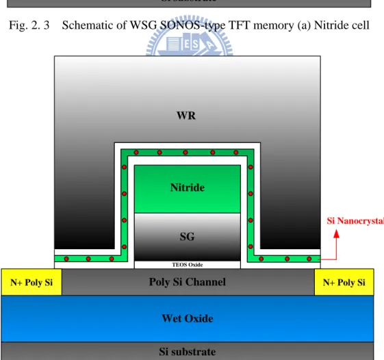
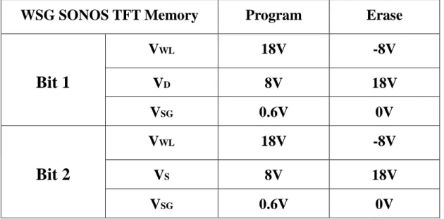
It is the first time we successfully fabricated Wrapped-Select-Gate SONOS-type memory on simulated glass substrate to be a thin-film-transistor (TFT) memory, First of all, silicon wafer with 5500 Å wet oxide were used as starting substrate. Then, a 500 Å amorphous Si (a-Si) film for the channel region was deposited at 500 oC by low-pressure chemical vapor deposition (LPCVD) and patterned by plasma dry etching. The deposited a-Si films were recrystallized by solid-phase-crystallization (SPC) at 600 oC for 24hr. To form inner assistant gate, we deposited 180 Å TEOS oxide, 1000 Å in-situ N+ ploy-Si layer, and 1000 Å nitride. The thick nitride layer above select gate is served as isolation between select gate and word-line gate. Subsequently lithography and etching was performed. After pattering select-gate structure, the tunnel oxide/trapping layer/blocking oxide stack layer was deposited as ONO-type dielectric layer. These thin film thickness are 180 Å , 120Å and 235Å respectively. In this experiment, trapping layer materials are pure nitride, nitride with embedded silicon nanocrystals [2.1] and N+ floating gate. Following the 2000 Å poly-Si deposition and word-line gate patterning, gate implant and source/drain region were formed by self-alignment technique. The cross-section of WSG-SONOS thin film transistor (TFT) memory device (a) Nitride cell (b) Nitride_Dot cell (c) Floating gate cell and examples of basic operation bias are shown in Fig. 2.3-2.5 and Table 2.1.
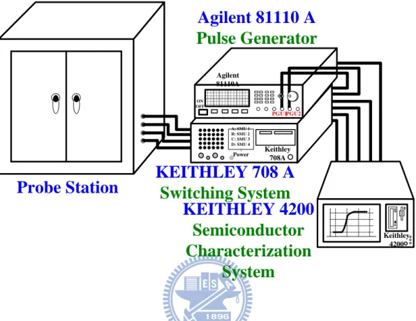
2.3 Measurement and Equipment Setup
Fig. 2.6 shows the connection of each measurement apparatus for I-V curve and
12
characterization system (KEITHLEY 4200), two channel pulse generator (Agilent 81110A), low leakage current switch mainframe (KEITHLEY 708A) and the probe station. Stable measuring environments provide us accurate electrical characteristics extraction.
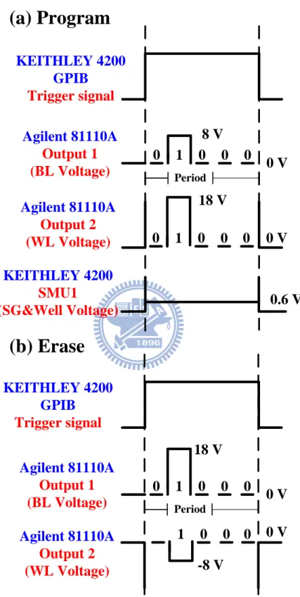
The timing diagrams of program and erase operation are shown in Fig. 2.7. KEITHLEY 4200 equipped with programmable source-monitor unit (SMU) and a high resolution current amplifier with pico-ampere range is the main control system here which is responsible for electrical characteristics measurement. Besides, Agilent 81110A with two pulse channels can not only offers us a high timing resolution pulse for P/E cycling in ordinary flash memory endurance test but also be used in every program and erase pulse. In order to obtain excellent ability to precisely control the pulse level and pulse timing of Agilent 81110A, the triggered pattern mode is used by the GPIB baseband between Agilent 81110A and KEITHLEY 4200. In our measurements, the duty cycle is 50% and the pulse period is set larger than100ns for better square pulse, while the both edge of rising time and falling time are larger than 25-50ns to prevent under-shoot and over-shoot from happening. Moreover, the C++ language is applied to take control of different equipment such as the low leakage current apparatus KEITHLEY 708A with 10-input and 12-output switching matrix which can automatically switch the signals to the device under test. That is why this measurement system empowers us to investigate different program/erase/read techniques in novel Wrapped-Select-Gate SONOS-type thin film transistor memory.
2.4 Operation of Program/Erase/Read
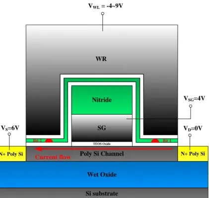
The WSG SONOS-type TFT memory was programmed and erased by applying source side injection [1.9] and band-to-band tunneling hot hole injection mechanism
13
respectively. The hot electrons were accelerated by high electric field in the gap region between word line gate and select gate. Under high word line gate bias, electrons which were accelerated due to horizontal electric field have larger injection efficiency to trapping layer compared to conventional channel hot electron injection, as shown in Fig. 2.8. The program condition is set at VWL = 18V, VBL = 8V, VSG =
0.6V. Secondly, the band-to-band tunneling hot hole injection mechanism is employed to neutralize electrons trapped in our different trapping layer materials. Under a reverse bias of the p-n junction, excess holes are generated and then are accelerated by lateral field. By gaining enough energy from electric field, these hot holes could easily overcome potential barrier height, jump into electron storage layer, and then recombine with electrons in trapping layer, as shown in Fig. 2.9. In the read mode, the sweeping voltage of word line gate is from -4V~9V, in the meanwhile, VBL and VSG
remain 6V and 4V respectively for better second bit effect characteristic. In order to perform two bit operation, forward read and reverse read are applied to confirm the state of Bit 1 and Bit 2, as shown in Fig. 2.10 and Fig. 2.11. In this work, threshold voltage (VT) is defined as the applied word line gate voltage when the sensing current
is 10-7 A in read mode. Memory window is defined as the VT shift between program
state and erase state.
2.5 Disturbance Characteristics
Fig. 2.12 shows two types disturbance of memory array during programming which called gate (word-line) disturbance and drain/source (bit-line) disturbance [2.2]-[2.3]. When Cell A is programmed, gate disturb takes place in Cell B and the drain disturb takes place in Cell C. Operation bias applied to neighboring un-selected cells might result in high electric field across gate dielectrics helping electrons to trap
14
or de-trap. The tunneling of electrons in these neighboring cells causes significant threshold voltage shift. Besides, there also exists another type of disturbance when we are reading a specific memory cell in the array which we called read disturbance [2.4]. These disturbance characteristics may restrain the feasibility of multi-level operation.
15
Substrate
D
S
Contral Gate
Nitride
Oxide
Oxide
Fig. 2. 1 Schematic of conventional two-bit SONOS-type memory
D
S
SG
Substrate
Bit 1
WL
Bit 2
16 Wet Oxide Si substrate Poly Si Channel SG TEOS Oxide N+ Poly Si N+ Poly Si Nitride WR
Fig. 2. 3 Schematic of WSG SONOS-type TFT memory (a) Nitride cell
Wet Oxide Si substrate Poly Si Channel SG TEOS Oxide Nitride Si Nanocrystal WR N+ Poly Si N+ Poly Si
17 Wet Oxide Si substrate Poly Si Channel SG TEOS Oxide N+ Poly Si N+ Poly Si Nitride WR N+ Floating Gate
Fig. 2. 5 Schematic of WSG SONOS-type TFT memory (c) Floating gate cell
WSG SONOS TFT Memory
Program
Erase
Bit 1
V
WL18V
-8V
V
D8V
18V
V
SG0.6V
0V
Bit 2
V
WL18V
-8V
V
S8V
18V
V
SG0.6V
0V
18 Keithley 4200 A: SMU 1 B: SMU 2 C: SMU 3 D: SMU 4 : Power ON OFF
Agilent 81110 A
Pulse Generator
KEITHLEY 708 A
Switching System
Probe Station
KEITHLEY 4200
Semiconductor
Characterization
System
Agilent 81110A PGU1PGU2 Keithley 708AFig. 2. 6 The experimental setup of each apparatus for pulse generator and I-V characteristics measurement of memory cell.
19
Operation Bias
1
0
0
0
0
8 V
0 V
KEITHLEY 4200
GPIB
Trigger signal
Agilent 81110A
Output 1
(BL Voltage)
Period(a) Program
1
0
0
0
0
18 V
0 V
KEITHLEY 4200
GPIB
Trigger signal
Agilent 81110A
Output 1
(BL Voltage)
(b) Erase
18 V
0 V
-8 V
0 V
Agilent 81110A
Output 2
(WL Voltage)
0
1
0
0
0
Agilent 81110A
Output 2
(WL Voltage)
1
0
0
0
PeriodKEITHLEY 4200
SMU1
(SG&Well Voltage)
0.6 V
Fig. 2. 7 The timing diagrams of the two-pulse generator, Agilent 81110A, during (a) program and (b) erase.
20 Wet Oxide Si substrate Poly Si Channel SG TEOS Oxide N+ Poly Si N+ Poly Si Nitride WR VWL=18V VD=8V VS=0V VSG=0.6V
Fig. 2. 8 Cross-sectional scheme of WSG-TFT memory during programming
Gate
N
+silicon
SiO2 SiO2 Nitride Hot Hole h+ h+e
-e
-e
-Trap Assist Tunneling21 Wet Oxide Si substrate Poly Si Channel SG TEOS Oxide N+ Poly Si N+ Poly Si Nitride WR VS=6V VD=0V VSG=4V VWL = -4~9V Bit 1 Bit 2 Current flow
Fig. 2. 10 The operation of reverse read Bit 1 in WSG-SONOS TFT memory cell.
Wet Oxide Si substrate Poly Si Channel SG TEOS Oxide N+ Poly Si N+ Poly Si Nitride WR VS=0V VD=6V VSG=4V VWL = -4~9V Bit 1 Bit 2 Current flow
22
Word Line
Word Line
Cell A Cell B
Cell C Cell D
Bit Line Bit Line
Fig. 2. 12 The circuit schematic of memory cells. When Cell A is programmed, gate disturb occurs in Cell B and the drain disturb occurs in Cell C.
23
Chapter 3
Characteristics of WSG-SONOS-type TFT memory
3.1 Introduction
In order to meet the emerging demand of portable electric products, we need a flash memory device with faster program speed, faster erase speed, smaller cell size, higher density, and the most importantly, reasonable sell prices. For this reason, high performance memory device and two bits per cell technique have been studied for a long time [3.1]-[3.3]. The main idea of this novel technique is that we have charges localized trapping in discrete storage trapping site near source side and drain side. Moreover, we can precisely determine two bit states in a flash memory cell by using reverse read technique.
In this chapter, we will discuss the mechanism of program and erase of wrapped-select-gate structure memory cell. Conventional schematic of program speed and erase speed is attained for different bias condition. Additionally, we find that VSG
also plays an important role in programming process of wrapped-select-gate thin film transistor memory device. Then we discuss the problems and challenges of 2nd bit effect by measuring in forward read and reverse read. The above discussions are carried into three types of trapping layer in our experiments.
3.2 Results and Discussions
For wrapped-select-gate SONOS-type TFT memory, we have two transistor characteristic in one cell which were controlled by word-line gate and select gate respectively. Fig. 3.1 - Fig. 3.3 show basic ID-VWL characteristics for three types of
24
WSG TFT memory. On the other hand, Fig. 3.4 - Fig. 3.6 show inner IDVSG
characteristics of Nitride-based (Nitride) cells, Nitride with Si dot (Nitride_Dot) cells, and N+ floating gate (Floating gate) cells. They have similar on/off ratio and threshold voltage in low drain voltage measurement. We additionally observe that Floating gate cell have serious floating gate coupling problem in Fig. 3.6. The off current is rise when VSG is larger than 8V.
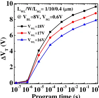
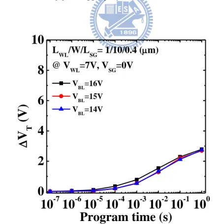
As mentioned before, split gate structure can offer a more effective way for electrons to tunnel into trapping layer that we called source side injection [3.4]. Fig. 3.7 shows program speed characteristics of Nitride cell with different word-line gate voltage. We can observe that VWL=18V case has the fastest speed for programming.
3V memory window can be achieved in few micro-second. The same results also occur in Nitride_Dot cell and Floating gate cell, as shown in Fig.3.8 and Fig. 3.9. Although having faster speed in short programming time, Floating gate cell cannot separate program operation for bit1 and bit2 due to floating gate coupling. That is to say, in this operation bias, Floating gate cell no longer has two bit per cell operation characteristics. So we also exhibit another operation bias for program in Fig. 3.10 which apparently has slower speed and acceptable 2nd bit effect with 2V memory window. In order to make it clear to understand where is the main injection location for electron tunneling by source-side-injection mechanism, the simulated electric field is performed both laterally and vertically, as shown in Fig.3.11 and Fig.3.12.. Channel region ranges from x=-0.5m to x=0.5m and voltage bias are set to be VWL=16~18V,
VBL=8V, and VSG=2V. We find that VWL=18V case has both strongest lateral and
vertical electric field in ONO gap between word-line gate and select gate. By increasing word-line gate voltage, the voltage difference between word-line gate and inversion layer increases. Thus, we have larger vertical electric field. At the same time,
25
the bit-line voltage becomes easier to couple into gap region by inversion region. In this way, higher voltage difference between two inversion regions gives rise to larger lateral electric field. That is why VWL=18V case shows the fastest program speed and
largest memory window.
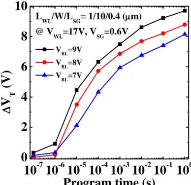
Let’s talk about the influence of bit-line voltage in program speed measurement. Voltage bias are set to be VWL=17V, VBL=7~9V, and VSG=0.6V. As shown in Fig. 3.13
to Fig. 3.15, the larger bit-line voltage is applied, the faster program speed we have. In order to attain acceptable two bit operation, junction breakdown injection mechanism was performed to single side programming, as shown in Fig. 3.16. Also, the results of simulated lateral and vertical electric field are shown in Fig. 3.17 and Fig. 3.18. When we increase bit-line voltage, higher voltage difference between word-line inversion and select gate inversion regions gives rise to larger lateral electric field. Besides, the voltage difference between word-line gate and its inversion region decreases which suppress vertical electric field of gap region.
In wrapped-select-gate structure memory, not only word-line gate voltage and bit-line voltage but also select gate voltage can control the programming current and electric field during program speed measurement. The following measurements are divided into two parts, large VSG (VSG=1, 2, 3 V) and small VSG (VSG=0, 0.4, 0.8 V).
Fig. 3.19 shows that large VSG could result in the suppression of electron tunneling
from channel to nitride trapping layer. However, in small VSG measurements, three
cases exhibit comparable program speed characteristics, as shown in Fig. 3.20. Without the suppression of electric field, programming current becomes dominant in these tests. We find that VSG=0V case still have equal programming current compared
to VSG=0.8V case due to large operation bias like VWL=18V and VBL=8V. The same
26
Fig. 3.24. Regarding the single side programming for Floating gate cell by junction breakdown injection mechanism, programming current no longer plays a key role in these measurements, as shown in Fig. 3.25 and Fig. 3.26. When select gate voltage is increased, both lateral and vertical are suppressed which give rise to slower program speed. The simulations of electric field are also carried out to demonstrate the influence of select gate voltage, as shown in Fig. 3.27 and Fig. 3.28.
In this thesis, we use reverse read and forward read techniques to determine the states of bit1 and bit2. However, traditional SONOS memory device exists the interference between two states we called 2nd bit effect [3.5]-[3.7]. Fig. 3.29 shows the interference between programmed bit1 and erased bit2 of WSG TFT memory Nitride cell. Threshold voltage variation of bit2 is smaller than 1V under applying VBL=6V
and VSG=4V. In this way, we indeed have memory window larger than 4V. Fig. 3.30
also shows the interference between programmed bit1 and erased bit2 of WSG TFT memory Nitride_Dot cell. Under reading voltage VBL=6V and VSG=4V operation,
Nitride_Dot still exhibits acceptable VT variation of bit2 although bit1 is programmed
to larger memory window. Based on single side programming, Floating gate cell also shows 2V memory window in spite of serious floating gate coupling effect, as shown in Fig. 3.31.
Erase operation is performed by band-to-band tunneling hot hole injection and junction breakdown mechanism. Holes are accelerated by large positive bit-line voltage and tunnel into trapping layer. Fig. 3.32 shows erase speed of WSG TFT memory Nitride cell with VWL=-6~-8V. We observe that VWL=-8V, VBL=18V, VSG=0V
case exhibits the fastest erase speed due to the largest tunneling opportunity resulting from vertical electric field. Fig. 3.33 shows the influence of VBL in erase speed
27
around junction region. As we expected, among three cases of VBL=16, 17, 18V,
VBL=18V shows the greatest erase ability, about 6V in one second. Fig. 3.34 and Fig.
3.35 show erase speed characteristics of WSG TFT memory Nitride_Dot cell with various word-line voltages and bit-line voltages. Compared to the results of Nitride cell, they have comparable erase speed in both measurements. For Floating gate cell, owing to floating gate coupling, they have faster erase speed in short erase time, as shown in Fig. 3.36 and Fig. 3.37. After measurement with different word-line bias and bit-line bias, we still need to confirm the hot holes injection location during erase. We observe that both lateral and vertical direction have large electric field peak right in the overlapped region of word-line gate and drain region, as shown in Fig. 3.38 and Fig. 3.39. However, operation bias of BTBTHH may lead to unwanted situation that bit 1 and bit 2 are erased at the same time. In order to achieve two bit operation, single side junction breakdown mechanism with smaller operation voltages is performed again with VWL=-8V, VBL=15V, and VSG=0V. Fig. 3.40 and Fig. 3.41 shows slower
erase characteristics of Floating gate cell with acceptable 2nd bit effect.
In the end of this chapter discussion, all programming and erase mechanism of different cells are listed in Table 3.1. Speed, 2nd bit effect, and endurance to 10K time P/E cycle are carried to comparison sheet.
3.3 Summary
Owing to the development of portable electronic devices, people are looking forward memory devices with fast program speed, fast erase speed, and high density characteristics. Wrapped-select-gate structure memory devices show excellent P/E speed with source-side injection and BTBTHH injection mechanism. Moreover, WSG structure memory devices also perform two bit operation exhibiting good immunity to
28
2nd bit effect. We also observe that the increase of word-line gate voltage will enhance both lateral and vertical electric field during programming. On the other hand, the increased bit-line voltage will enhance lateral electric field but suppress vertical electric field at the same time. For erase operation, bit-line voltage is responsible for generation of excess holes while word-line voltage take charge of tunneling efficiency. Among three types of WSG TFT memory, Floating gate cell suffers serious floating gate problems. Nitride cell and Nitride_Dot cell show great potential to scaling down and outstanding P/E characteristics.
29 -4 -2 0 2 4 6 8 10-12 10-11 10-10 10-9 10-8 10-7 10-6 10-5 10-4 L WL/W/LSG=1/10/0.4 (m) @VBL=0.1V I D (A) VWL (V) VSG=0V VSG=4V
Fig. 3. 1 The ID-VG characteristics of WSG SONOS-type TFT memory with
Nitride trapping layer on the different select gate voltage
-4 -2 0 2 4 6 8 10-12 10-11 10-10 10-9 10-8 10-7 10-6 10-5 10-4 I D (A) VWL (V) VSG=0V VSG=4V L WL/W/LSG=1/10/0.4 (m) @V BL=0.1V
Fig. 3. 2 The ID-VG characteristics of WSG SONOS-type TFT memory with
Nitride + Si dot trapping layer on the different select gate voltage
-4 -2 0 2 4 6 8 10-12 10-11 10-10 10-9 10-8 10-7 10-6 10-5 10-4 I D (A) VWL (V) VSG=0V VSG=4V L WL/W/LSG=1/10/0.4 (m) @V BL=0.1V
Fig. 3. 3 The ID-VG characteristics of WSG SONOS-type TFT memory with
30 -4 -2 0 2 4 6 8 10-12 10-11 10-10 10-9 10-8 10-7 10-6 10-5 10-4 I D (A) VSG (V) VWL=0V VWL=6V L WL/W/LSG=1/10/0.4 (m) @V BL= 0.1V
Fig. 3. 4 The ID-VSG characteristics of WSG SONOS-type TFT memory with
Nitride trapping layer on the different select gate voltage
-4 -2 0 2 4 6 8 10-12 10-11 10-10 10-9 10-8 10-7 10-6 10-5 10-4 I D (A) VSG (V) VWL=0V VWL=6V L WL/W/LSG=1/10/0.4 (m) @V BL= 0.1V
Fig. 3. 5 The ID-VSG characteristics of WSG SONOS-type TFT memory with
Nitride + Si dot trapping layer on the different select gate voltage
-4 -2 0 2 4 6 8 10-12 10-11 10-10 10-9 10-8 10-7 10-6 10-5 10-4 I D (A) VSG (V) VWL=0V VWL=6V L WL/W/LSG=1/10/0.4 (m) @V BL= 0.1V
Fig. 3. 6 The ID-VSG characteristics of WSG SONOS-type TFT memory with
31
10
-710
-610
-510
-410
-310
-210
-110
00
2
4
6
8
10
V
T(V)
Program time (s)
L WL/W/LSG= 1/10/0.4 (m) VWL=18V VWL=17V VWL=16V @ VBL=8V, VSG=0.6VFig. 3. 7 Program speed characteristics of WSG SONOS-type TFT memory with Nitride trapping layer on the various word line bias
10
-710
-610
-510
-410
-310
-210
-110
00
2
4
6
8
10
L WL/W/LSG= 1/10/0.4 (m)
V
T(V)
Program time (s)
VWL=18V VWL=17V VWL=16V @ VBL=8V, VSG=0.6VFig. 3. 8 Program speed characteristics of WSG SONOS-type TFT memory with Nitride + Si dot trapping layer on the various word line bias
32
10
-710
-610
-510
-410
-310
-210
-110
00
2
4
6
8
10
V
T(V)
Program time (s)
L WL/W/LSG= 1/10/0.4 (m) VWL=18V VWL=17V VWL=16V @ VBL=8V, VSG=0.6VFig. 3. 9 Program speed characteristics of WSG SONOS-type TFT memory with N+ floating gate trapping layer on the various word line bias
10
-710
-610
-510
-410
-310
-210
-110
00
2
4
6
8
10
V
T(V)
Program time (s)
L WL/W/LSG= 1/10/0.4 (m) VWL=8V VWL=7V VWL=6V @ VBL=15V, VSG=0VFig. 3. 10 Program speed characteristics of WSG SONOS-type TFT memory Floating gate cell on the various word line bias exhibiting acceptable 2nd bit effect
33
-1.0
-0.5
0.0
0.5
1.0
0.0
0.2
0.4
0.6
0.8
1.0
VWL=16V VWL=17V V WL=18V LWL/W/LSG=1/10/0.4 (m) @VBL=8V, VSG=2VLater
al Elec
tric F
ield (
MV/c
m)
Lateral Distance (m)
Fig. 3. 11 The simulated results of lateral electric field start from VWL=16V to
VWL=18V in the channel of WSG SONOS TFT memory device
-1.0
-0.5
0.0
0.5
1.0
0.0
0.2
0.4
0.6
0.8
1.0
Ver
tical Electric
F
ield (
MV/c
m)
Lateral Distance (m)
VWL=16V V WL=17V V WL=18V L WL/W/LSG=1/10/0.4 (m) @VBL=8V, VSG=2VFig. 3. 12 The simulated results of vertical electric field start from VWL=16V to
34
10
-710
-610
-510
-410
-310
-210
-110
00
2
4
6
8
10
V
T(V)
Program time (s)
L WL/W/LSG= 1/10/0.4 (m) VBL=9V VBL=8V VBL=7V @ VWL=17V, VSG=0.6VFig. 3. 13 Program speed characteristics of WSG SONOS-type TFT memory with Nitride trapping layer on the various bit line bias
10
-710
-610
-510
-410
-310
-210
-110
00
2
4
6
8
10
V
T(V)
Program speed (s)
LWL/W/LSG= 1/10/0.4 (m) VBL=9V VBL=8V VBL=7V @ V WL=17V, VSG=0.6VFig. 3. 14 Program speed characteristics of WSG SONOS-type TFT memory with Nitride + Si dot trapping layer on the various bit line bias
35
10
-710
-610
-510
-410
-310
-210
-110
00
2
4
6
8
10
V
T(V)
Program time (s)
L WL/W/LSG= 1/10/0.4 (m) VBL=9V VBL=8V VBL=7V @ VWL=17V, VSG=0.6VFig. 3. 15 Program speed characteristics of WSG SONOS-type TFT memory with N+ floating gate trapping layer on the various bit line bias
10
-710
-610
-510
-410
-310
-210
-110
00
2
4
6
8
10
V
T(V)
Program time (s)
L WL/W/LSG= 1/10/0.4 (m) VBL=16V VBL=15V VBL=14V @ VWL=7V, VSG=0VFig. 3. 16 Program speed characteristics of WSG SONOS-type TFT memory Floating gate cell on the various bit line bias exhibiting acceptable 2nd bit effect
36
-1.0
-0.5
0.0
0.5
1.0
0.0
0.2
0.4
0.6
0.8
1.0
VBL=7V VBL=8V V BL=9V LWL/W/LSG=1/10/0.4 (m) @VWL=17V, VSG=2VLater
al Elec
tric F
ield (
MV/c
m)
Lateral Distance (m)
Fig. 3. 17 The simulated results of lateral electric field start from VBL=7V to
VBL=9V in the channel of WSG SONOS TFT memory device
-1.0
-0.5
0.0
0.5
1.0
0.0
0.2
0.4
0.6
0.8
1.0
Ver
tical
Elec
tric F
ield (
MV/c
m)
Lateral Distance (m)
VBL=7V V BL=8V V BL=9V L WL/W/LSG=1/10/0.4 (m) @VWL=17V, VSG=2VFig. 3. 18 The simulated results of vertical electric field start from VBL=7V to
37
10
-710
-610
-510
-410
-310
-210
-110
00
2
4
6
8
10
V
T(V)
Program time (s)
L WL/W/LSG= 1/10/0.4 (m) VSG=3V VSG=2V VSG=1V @ VWL=18V, VBL=8VFig. 3. 19 Program speed characteristics of WSG SONOS-type TFT memory with Nitride trapping layer on the large select gate bias
10
-710
-610
-510
-410
-310
-210
-110
00
2
4
6
8
10
V
T(V)
Program time (s)
LWL/W/LSG= 1/10/0.4 (m) VSG=0.8V VSG=0.4V VSG=0V @ VWL=18V, VBL=8VFig. 3. 20 Program speed characteristics of WSG SONOS-type TFT memory with Nitride trapping layer on the small select gate bias
38
10
-710
-610
-510
-410
-310
-210
-110
00
2
4
6
8
10
V
T(V)
Program time (s)
L WL/W/LSG= 1/10/0.4 (m) VSG=3V VSG=2V VSG=1V @ VWL=18V, VBL=8VFig. 3. 21 Program speed characteristics of WSG SONOS-type TFT memory with Nitride + Si dot trapping layer on the large select gate bias
10
-710
-610
-510
-410
-310
-210
-110
00
2
4
6
8
10
V
T(V)
Program time (s)
LWL/W/LSG= 1/10/0.4 (m) VSG=0.8V VSG=0.4V VSG=0V @ VWL=18V, VBL=8VFig. 3. 22 Program speed characteristics of WSG SONOS-type TFT memory with Nitride + Si dot trapping layer on the small select gate bias
![Table 1. 1 Non-volatile Memory Technology Requirements for NOR Flash in ITRS 2010 Edition _ Process Integration, Devices, and Structures [1.4]](https://thumb-ap.123doks.com/thumbv2/9libinfo/8751333.205990/23.892.127.774.754.1038/volatile-technology-requirements-edition-process-integration-devices-structures.webp)