國 立 交 通 大 學
電子工程學系電子研究所
博 士 論 文
高頻被動元件在矽基板和多層介電質基板之模
型與特性
The Characteristics and Models of High Frequency
Passive Devices on Silicon and PCB Substrates
研 究 生 :陳家忠
指導教授 :荊鳳德 博士
高頻被動元件在矽基板和多層介電質基板之模型與特性
研究生:陳家忠
指導教授:荊鳳德教授
國立交通大學電子工程系電子研究所
摘要
隨著行動無線通訊系統需求日益增加,對高性能、低成本、低功率、以及 小體積之射頻/微波電路之需要更顯得迫切。由於現今積體化之CMOS 晶片不斷 地微縮化,使得主動元件可震盪頻率不斷地提高,若再能結合高性能化的高頻被 動元件,會使得CMOS 矽製程儼然成為可應用於射頻/微波領域的半導體技術之 一,故改善高頻被動元件特性為其研究之重點。 然而,CMOS 製程所使用之標準低阻值矽基板 (ρ ~10 Ω-cm) 而言,其上 的傳輸線以及被動元件皆有著相當高的訊號損失。這些損失不但造成元件本身特 性變差,更會破壞CMOS 射頻/微波電路的效能。這些低性能的被動元件,正是 目前CMOS 射頻/微波電路最大的致命傷之一。因此,如何克服此問題,對未來 CMOS 射頻/微波電路的研究與發展將有著關鍵性的影響。 本論文中首先採用高阻值的矽基板,來降低其上元件之訊號在基板中的損 耗,進而提升射頻/微波性能及改善 CMOS 射頻/微波電路系統之特性,並能使 用 3D 之技術能來整合被動元件在同一晶片中,也是最終之目的。此外,也針對 在多層介電板中之高頻被動元件,利用半導體之製程技術來改善其高頻特性,因 為現今高頻被動元件都仍外掛於晶片外中在印刷電路板中,改善其元件效能,也是本篇聚焦之貢獻。
本論文以射頻/微波電路中最常見之收發器 (transceiver) 電路出發,架構分 別為:高頻被動元件在矽基板之研究; 高頻被動元件在多層介電板之研究;傳輸 線在晶片中損耗的影響; 及結合 3D 技術整合微波被動元件四方面來探討。包 括:共平面 (CoPlanar Waveguide, CPW) 傳輸線、 微波帶通 (band-pass); 分 散式 (distributed) 濾波器,耦合器(Couplers)元件等等;最後亦探討了晶片內之傳 輸和整合被動元件於晶片系統中。研究內容主要在於基板阻值對元件特性的影 響,包括功率耗損、頻寬的延伸、能量的傳輸,和低耗損的共振。最後,仍朝著
結合這些被動元件於收發器電路中,作出高性能高度整合之 CMOS 收發器為目
The Characteristics and Models of High Frequency Passive
Devices on Silicon and PCB Substrates
Student: C. C. Chen Advisor: Prof. Albert Chin
Department of Electronics Engineering & Institute of Electronics National
Chiao-Tung University
Abstract
As mobile microwave communication development increases, high performance, low-cost, low power, small size RF integrated circuits (RFICs) are required. This is because the maximum oscillation frequency increases as down-scaling CMOS technology (for 90 nm RF CMOS). However, transmission lines and passive circuit components on standard low-resistivity silicon substrates such as those used in CMOS processing have high power loss, which degrade the characteristics of devices and further damage the performance of CMOS RF/Microwave circuits. To overcome this problem, we have developed a method of high resisvity silicon substrate technology, which is capable of converting the standard low-resistivity Si to high-resistivity for large substrate loss improvement with full VLSI technology process compatibility.
In this work, we have applied the high-resistivity Silicon substrate to almost all of the passive components used in a common transceiver on Si, including: coplanar
filters and couplers. In addition, the standard VLSI process is used to improve RF characteristics on high frequency printed circuit board (PCB) passive devices. The superior RF characteristics of extending bandwidth, lower insertion loss, and high coupling correspond with advanced wireless system demands. Hence, we have successfully demonstrated the excellent characteristics of RF passive devices on both silicon substrate and printed circuit board by decreasing power and coupling losses. Moreover, with the development of three dimensional technology, combing with interconnects and high resistivity substrate, these passive devices on standard VLSI process have been embedded into ICs. These device characteristics on silicon or PCB substrates, such as measured power loss, bandwidths, return loss, and insertion loss and coupling effect have presented in whole chapters. These enhanced RF performance methods on RF passive devices can contribute to applications in the advanced wireless systems.
ACKNOWLEDGMENTS
I would first like to thank my adviser Prof. Albert Chin for his illuminativesuggestions and discussions during the period of my working toward PhD degree. His inspiration benefits me a lot on the creative ideas, effective schedule control and the integrity to the processing tasks. And I must say thanks to Prof. J. T. Kuo in Dept. of Communication Eng., National Chiao Tung University (NCTU), for the precious instructions and supports on the filters and couplers research.
I appreciate the financial and equipment supports from National Science Council (NSC 94-2215-E-009-062), National Nano Device Lab. and Semiconductor Center of NCTU. I am also grateful to those who ever assisted this work: the crew of ED633 Lab. (especially to, H. L. Kao, B. F. Hung, C. H. Chen, C. H. Lai, and K. C. Chiang ); Mr. Meshon Jiang at Dept. of Communication Eng., NCTU for the filter work.
Finally, much gratitude must be expressed to Dept. of Electronics Eng., NCTU, for the 4-year training, to my dear friends for the encouragement and to my family who always support me and give me all their love. This work can’t be finished without them.
CONTENTS
ABSTRACT
iACKNOWLEDGMENTS
viCONTENTS
viiiFIGURE CAPTIONS
xiiTABLE CAPTIONS
xxiiiCHAPTER
1
INTRODUCTION
11.1 Si Substrate for RF CMOS Technology
11.2 PCB Substrate for High-Speed
Circuit
41.2.1 Printed Circuit Board Substrate 4
1.2.2 PCB Process Limitation 5
1.3 Backend Interconnect and Integrated with 3D
7CHAPTER 2 Transmission Lines and Ring
resonators
92.1 Bulk and Thin-Film Microstrip Transmission Lines on
VLSI-Standard
Si
Substrates
92.1.3 Thin-film Microstrip Lines on Si 11
2.1.4 Experimental Procedure 11
2.1.5 Conclusion 12
2.2 CPW and Microstrip Ring Resonators on Silicon
Substrates
14
2.2.1 Motivation 14
2.2.2 Design Process 15
2.2.3 Experimental Results 16
2.3
Modeling
and
Mechanisms
18
2.3.1 Analysis from Modeling 18
2.4 Conclusions
21CHAPTER 3 Microwave Filters and Couplers
323.1 Microwave Band-Pass Filters on PCB
323.1.1 Motivation 32
3.1.2 Filter Design and Fabrication 33
3.1.3 Results and Discussion 36
3.1.4 Conclusions 37
3.2 Microwave Couplers on PCB
383.2.1 Motivation 38
3.2.2 Filter Design and Fabrication 39
3.2.3 Results and Discussion 40
3.2.4 Conclusions 42
CHAPTER 4 Coupling and dynamic power
losses in VLSI interconnects
52
4.1. AC Power Loss and Signal Coupling
524.1.1 Motivation 52
4.1.2 Experimental Procedure 53
4.2 1-Poly-1-Metal 0.18-
µm Si MOSFETs
554.2.1 Results and Discussion 55
4.3 1-Poly-6-Metal 0.18-
µm Si MOSFETs
574.3.1 Results and Discussion 57
4.3.2 Signal Coupling loss and Power Loss 57
4.4 Conclusions
59CHAPTER 5 Band-Pass Filter on 3D VLSI
69
5.1
Band-Pass Filter Using VLSI Backend Interconnects 695.1.1 Motivation 69
5.1.2 Filter Design and Fabrication 70
5.1.3 Results and Discussion 71
5.1.4 Equivalent Circuit Model 72
5.1.5 Conclusions 74
CHAPTER 6 CONCLUSIONS AND FUTURE
WORKS
836.1 Conclusions
83
REFERENCES
86VITA
99
FIGURE CAPTIONS
Fig. 2.1.1 The measured and EM-simulated power loss of 3 mm long bulkmicrostrip transmission lines. For comparison, results for a 1 mm long CPW line are included. Implantation produces a large loss reduction, from 6.7 dB/mm to 0.4 dB/mm at 50 GHz
Fig. 2.1.2 The measured and EM-simulated power loss of 0.75 mm long thin-film microstrip transmission lines. The measured loss at 20 GHz is < 1 dB/mm, i.e. much lower than the bulk CPW (3 dB/mm) and microstrip lines (6 dB/mm) in Figure 1 without implantation.
Fig. 2.2.1 Images of fabricated (a) CPW and (b) microstrip ring resonators designed at 40 GHz and 30 GHz, respectively. The long surrounded stubs near the ring are to enhance the coupling efficiency.
Fig. 2.2.2 The measured S-parameters of CPW ring resonators (a) with and (b) without proton implantation. The EM and circuit simulated filter characteristics are shown for reference.
Fig. 2.2.3 The measured S-parameters of 30 GHz microstrip line ring resonators (a) with and (b) without proton implantation. The EM-simulated and the equivalent circuit simulated filter characteristics are also shown for
reference. No resonance is observed in (b) due to the substrate loss of ~40 dB.
Fig. 2.3.1 The physically-based equivalent circuit for the microstrip transmission lines. The Lt represents the line inductor, and Rt the parasitic resistor of the transmission line. The substrate loss is modeled by the shunt Rs and Cs to ground.
Fig. 2.3.2 The measured and equivalent-circuit modeled S-parameters of (a) bulk and (b) thin-film microstrip transmission lines on Si substrates. The effect of proton implantation is shown in (a). The different curve lengths are due to different frequency ranges: 50 GHz in (a) and 20 GHz in (b). Fig. 2.3.3 The extracted magnitude of the substrate-impedance/mm derived from
the bulk and thin-film microstrip transmission lines. The effect of proton implantation is to increase the substrate impedance and thus reduce the loss of the bulk microstrip transmission line.
Fig. 2.3.4 The physically-based equivalent circuit of ring resonators. The L expresses the metal stub, and the C1 is the fringing coupling capacitance
of the ring. The substrate loss is modeled by the shunt Rs and Cs to ground.
Fig. 2.3.5 The extracted magnitude of the substrate impedance from (a) CPW ring resonators and (b) microstrip ring resonators with or without implantation. The substrate impedances were increased by the implantation, reducing the insertion loss of the ring resonators.
Fig. 3.1.1 Structure of a dual-mode ring resonator filter.
Fig. 3.1.2 Normalized frequencies foe/fo and foe/fo as a function of electrical length 2θp.
Fig. 3.1.3 Simulated responses of the dual-mode ring resonator filter with center frequency fc = 1.9 GHz. (a) Coupled gap = 240 µm, ∆ = 10%. (b) Coupling gap = 40 µm, ∆ = 30%.
Fig. 3.1.4 The dual-mode ring resonator filter with center frequency fc = 1.9 GHz. (a) Coupled gap = 240 µm, ∆ = 10%. (b) Coupling gap = 40 µm, ∆ = 30%.
Fig. 3.2.1 The fabricated coupler. (a) Photo of the entire circuit. (b) Enlarged picture of the coupled lines
Fig. 3.2.2 The measured and simulated responses of the fabricated Device 1. (a) |S21| (through) and |S31| (coupling). (b) |S11| (return loss) and |S41|
Fig. 3.2.3 The measured and simulated responses of the fabricated Device 2. (a) |S21| (through) and |S31| (coupling). (b) |S11| (return loss) and |S41|
(isolation)
Fig. 4.1.1 (a) The VLSI device integration scheme for Germanium-on insulator devices on a Si technology showing multi-level parallel interconnect lines. The AC power consumption in the parasitic CRL (Cv2f/2, Li2f/2, and i2Rf/2) can be simulated by using the two parallel long lines as in (b). The 3D device integration in (a) is equivalent to folding the 2D IC into 3D as in (b).
Fig. 4.1.2 Images of fabricated parallel lines with (a) 2 µm and (b) 10 µm width and 1 mm length. The CPW layout and 150 µm pitch probing pads are used for RF measurements.
Fig. 4.2.1 The measured and simulated (a) S21, (b) S11 and (c) power loss up to 20
GHz of 1 mm and 0.25 mm long parallel interconnect lines on 6 µm SiO2-isolated Si substrates. The line spacing was 2 µm.
Fig. 4.3.1 The measured and simulated (a) S21, (b) S11 and (c) power loss up to 20
GHz of 1 mm and 0.25 mm long parallel interconnect lines on 6 µm SiO2-isolated Si substrates. The line spacing was 2 µm.
CMOS circuits
Fig. 5.1.2 The measured and simulated S21 and S11 results of 1 mm coupled-line on
M1.
Fig. 5.1.3 The measured S21 and S11 results of a 1 mm coupled-line with 2.5 µm, 5
µm, and 10 µm spacings on M6.
Fig. 5.1.4 The measured and simulated S21 and S11 results of a 1 mm coupled-line
on M1 and M6 with HRS.
Fig. 5.1.5 The equivalent circuit of coupled-lines using interconnects on VLSI process.
Fig. 5.1.6 The measured and modeled S21 and S11 results of 1mm coupled-lines on
LRS.
Fig. 5.1.7 The measured and modeled S21 results of 1mm coupled-lines on HRS.
TABLE CAPTIONS
Table 3.2.1. Performance of the fabricated coupler at design frequencyfO=5GHZ.Table 4.2.1 Measured and simulated values of S21 and the Power loss at 20 GHz for
various structures having 1 or 0.25 mm lengths. The spacing of the lines were 2 or 10 µm and the thicknesses of the oxide were 0.7 µm or 6 µm,. HRS: High resistance substrate. Decreasing the line length by 1/4 can reduce the unwanted S21 coupling by more than 10 dB and is much more
Chapter 1
INTRODUCTION
1.1 Si Substrate for RF CMOS Technology
Millimeter-wave frequencies are being proposed for high-volume low-cost/ small size/ mass commercial communication applications. These applications include sensors for vehicle monitoring and control, local radio area networks (LAN’s), secure cellular-radio systems and short-range wide-band radio. To achieve low cost with moderate-to-high-volume circuit production, monolithic circuitry is preferred. At microwave frequencies monolithic microwave integrated circuit (MMIC’s) employ GaAs technology with integrated active devices. However, GaAs real estate is expensive, especially when passive devices occupying large areas are required, e.g., filters, couplers, diplexers, and antennas, etc.
A number of alternative substrates can be considered for planar millimeter-wave circuits or interconnect designs. Silicon technology is expected to be an effective strategy instead of GaAs. However, RF CMOS circuits suffer from
substrate and power losses. Besides, significant coupling effects may occur between parallel conductive lines or nearby devices due to the low substrate resistivity. The large RF signal leakage may damage the circuit performance through the parasitic capacitance of the conductive substrate. These drawbacks definitely increase the difficulties in designing Si CMOS RFICs and also limit the expansion of CMOS circuits for RF applications [1.1.1].
In order to overcome these problems, several methods have been explored, including: using high resistivity silicon [1.1.2], sapphire [1.1.3], silicon-on-insulator (SOI) wafers [1.1.4], thick oxide isolation layers, micromachined structures [1.1.5]-[1.1.6], silicon-metal-polymide (SIMPOL) structures [1.1.7] and porous Si [1.1.8]. The cost of Sapphire is expensive [1.1.9] and processes variations are difficult to control. The isolation for RF crosstalk on SOI and thick oxide isolation layer are constrained by process limitations, and becomes worse especially at higher frequencies. Micromachined, SIMPOL structures and porous Si suffer from incompatibility with CMOS processes. The high process costs and difficulties of integration with modern VLSI technology are serious drawbacks of these methods.
In order to overcome this technological challenge, we have used high resistivity silicon substrates to selectively convert the standard Si (10 Ω-cm) to high resistivity substrates with full current VLSI technology process. The major advantage of the high
resistivity silicon substrates is its simplicity and low cost. And, it has been reported that transmission lines on silicon substrate material have acceptable RF losses even in the microwave-frequency regime.
Based on this technology, we demonstrated the effectiveness of the high resistivity silicon substrates for reducing RF substrate loss in the Si passive devices, such as CoPlanar Waveguide (CPW) transmission lines, couplers, distributed broad-band band-pass filters, which are very important components for fully integrated Si RF transceivers. The novelty of using VLSI backend interconnect with high resistivity substrate also provides an attractive solution for RF passive devices embedded into low-cost high-performance wireless systems.
1.2 PCB Substrate for High-Speed circuit
1.2.1 Printed Circuit Board Substrate
The printed circuit board (PCB) used to physically mount and connect the circuit components in a high frequency product will have a significant impact on the performance of that product [1.2.1]. The potential magnitude of the effect of the PCB design increases with frequency as the parasitic elements tend to a similar magnitude to the typical lumped components used [1.2.2]. This leads to the requirement for increased inclusion of electrical models representing PCB structures into the circuit simulation. In practical radio products the requirements on the PCB design can sometimes be in conflict with ‘best manufacturing’ practice. In order to achieve the most optimum solution in all respects the radio designer, the PCB designer and the manufacturing engineer must all have some appreciation of each others requirements [1.2.3]. The most common processes used in the fabrication of PCBs are drilling, plating, bonding and etching [1.2.4]. Some new developments are underway where lasers are utilized to distinguish conducts. The principle advantage of this development has the ability to use smaller dimensioned features including track widths down to 0.05 mm. In all the lowest cost radio products multilayer PCBs are used and these comprise of a number of laminates of boards individually etched and
conductor layers reducing the required board space. Also, the type of via structure used will have a major effect on the processes required to fabricate the PCB and consequently the cost of the finished board [1.2.5]-[1.2.6].
1.2.2 PCB Process Limitation
In order to design a product using a PCB, it is important to understand the practical limitations of the fabrication process [1.2.7]. The manufacturing processes were used to etch the tracks, drill the holes and assemble the laminates have limitations. Exceeding these limitations will significantly increase the cost of the PCB as manufacturing yields reduce. The typical minimum limit on track thickness for a high volume, complex product is around 0.2 mm. A similar minimum limitation applies to the minimum gap between two different conducts. Some PCB manufacturers offer to etch track widths down to 0.125 mm. The minimum via hole size was used that can be drilled as a stack. It will have a significant effect on the cost of the board as the via hole size limits the number of PCBs. Not withstanding the radio performance implications of small diameter via holes, typical minimum sizes of 0.25 mm are commonly used.
In this paper, we present that the improved process flow to product the good performance on printed circuit board by lithography technology on VLSI. It can fabricate the passive devices without the problems of via-hole and designing. The
scaling gap-spacing and conductor width can help the designers to design wider range and product better RF characteristics. The original process limitation to product devices on PCB can be solved.
1.3 Backend Interconnect and Integrated with 3D
The strong demand on advanced wireless communication services for advanced system-on-a-chips has attracted a great deal of attention [1.3.1]. This is due to their significant benefits such as overall chip size reduction, lower fabrication cost, as well as enhanced system performance. Meanwhile, significant progress in advanced VLSI technology has made it possible to realize system-on-a-chip at millimeter-wave frequencies with three-dimensional technology [1.3.2]. The concept of integrating parallel coupled-line filters with CMOS integrated circuit on silicon (Si) substrate is appealing because shorter coupling-line has shown on backend local or globe interconnects with CMOS scaling down. This requirement becomes even more urgent as the operation frequency of Si communication integrated circuits (ICs) increases. However, the performance of microwave filters integrated on Si suffers from the high frequency losses and crosstalk of the low resistivity Si substrate. For local lines (especially in array structures such as cache RAMs) a key limitation is cross-talk. Cross-talk will progressively become worse in the future because of the increasing coupling capacitance among neighboring lines. Therefore, we study the test structure of coupled-line interconnect in ULSIs for measuring and characterizing of multi-layered interconnect capacitance. With the high resistivity silicon substrate, the substrate coupling successfully can be reduced; therefore, improving the RF
characteristics, the superior performance of the passive devices can be used as advanced millimeter-wave wireless communication systems.
Chapter 2
Transmission Lines and Ring
Resonators
2.1
Bulk and Thin-Film Microstrip Transmission Lines on
VLSI-Standard Si Substrates
2.1.1 Motivation
Scaling of Si device technology into the nm-scale regime yields Si transistors with performance reaching into the sub-THz range [2.1.1]. However, the performance of MMICs on Si substrates is inferior to those on semi-insulating GaAs (~107 Ω-cm) owing to the large loss of passive devices on the low resistivity Si (10 Ω-cm) substrates [2.1.2]-[2.1.3]. To overcome this problem, we have previously proposed and demonstrated a method to reduce the large RF loss in standard Si substrates using ion implantation which can selectively form high resistivity (106 Ω-cm) regions in VLSI-standard Si substrates (10 Ω-cm) [2.1.4]-[2.1.7]. Excellent coplanar waveguide (CPW) transmission lines with only 0.6 dB loss at 110 GHz [2.1.8] as well as
CPW-based broadband filters with small insertion loss (1.6 dB) and 10 GHz bandwidth at 91 GHz [2.1.9]- [2.1.10] have been demonstrated using this technique. In this section, we have successfully demonstrated high performance microstrip lines on Si substrates. Using ion implantation of proton, the power loss of the microstrip transmission line was reduced significantly from 6.7 dB/mm to only 0.4 dB/mm at 50 GHz. In addition, we have also fabricated thin-film microstrip transmission lines using current VLSI backend interconnect processes with a loss of ~0.9 dB/mm at 20 GHz. This approach has the inherit merit of being fully compatible with current VLSI technology without requiring additional masks or process steps.
2.1.2 Design Process
Standard 10 Ω-cm resistivity Si wafers with 200 µm thickness were used in this study. Bulk microstrip transmission lines were fabricated on 1.5-µm-SiO2/Si
substrates using 4 µm thick Al with 3 mm long and 60 µm wide. Thick Al was deposited on the backside of the wafer to form the bulk microstrip transmission line. For thin-film microstrip transmission lines, a 0.75 mm length and 20 µm width strip was formed using the top metal layer (metal-6) of a conventional VLSI backend process with the first metal layer used as the ground plane. Two-port S-parameters were measured up to 50 GHz using an HP8510C network analyzer.
2.1.3 Bulk Microstrip Lines on Si
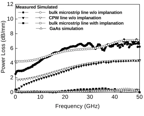
Figure 2.1.1 shows the power loss for a 3 mm long microstrip line on 1.5 µm SiO2-isolated Si, where the loss increases from 2.8 dB/mm to 6.7 dB/mm as the
frequency increases to 50 GHz. This loss is greater than that of the CPW transmission line, as shown in Figure 2.1.1, over the same frequency range. The larger loss in the microstrip transmission line than in the CPW line is due to the vertical EM field being fully inside the lossy Si substrate, whereas the horizontal EM field in CPW line is only partially within the Si substrate.
The increasing power loss at high frequency is an issue for Si RF IC technology since future wireless communications require higher frequencies and bandwidths. As shown in Figure 2.1.1, our microstrip transmission lines with proton implantation show an improved power loss of ≤ 0.4 dB/mm at 50 GHz. This value is similar to that of CPW transmission lines with the same ion implantation [6, 8] and comparable to the loss in semi-insulating GaAs obtained from EM simulation using IE3D.
2.1.4 Thin-film Microstrip Lines on Si
Using the same approach of forming a high resistivity layer by proton implantation, we have also designed and fabricated thin-film microstrip transmission lines. The isolation layer is from the multiple layers of SiO2 used in the VLSI backend
seen, the power loss is ~0.9 dB/mm at 20 GHz which is much lower than that of the un-implanted bulk CPW and microstrip lines shown in Figure 1. Although the loss of thin-film microstrip line at 20 GHz is larger than the 0.25 dB/mm in ion-implanted bulk microstrip lines, this process used simple layout technology without adding additional mask and process.
Because the transmission line is a passive device, the RF loss (L) is equivalent to the generated noise with equivalent noise temperature by (L-1)T0. The noise from
advanced 0.18 and 0.13 µm MOSFETs is ~2.5 dB at 20 GHz, whereas the un-implanted CPW and microstrip transmission lines typically show larger noise and would dominate the overall noise floor of an RF system. However, the noise floor can be significantly reduced by using the thin-film microstrip line, even for a length as long as 1 mm. Further improvement may be possible by improving the dielectric loss of the low-temperature-formed SiO2 or by increasing the thickness of the dielectric
layer. This will be possible using the advanced 1-poly-9-metal layer (1P-9M) process of the 90 nm technology node and beyond. This will further reduce the performance gap with the bulk microstrip transmission line using proton implantation or that on GaAs, with the inherit merit of only changing the layout of current VLSI.
GHz) and thin-film (0.9 dB/mm at 20 GHz) microstrip transmission lines on VLSI-standard Si substrates. Proton implantation selectively transforms the low resistivity Si substrates of bulk microstrip transmission line into a high resistivity state. The high performance of thin-film microstrip line results from the high-resistivity SiO2-dielectric being inside the microstrip line body. Both transmission lines can be
integrated into RF circuits and distributed devices at a reduced size compared with using CPW lines.
2.2
CPW and Microstrip Ring Resonators on Silicon
Substrates
2.2.1 Motivation
Integrated ring resonators are desirable due to their compact size, low cost, and easy fabrication. Owing to the narrow passband bandwidth and low radiation loss, ring resonators have been applied to band-pass filters, oscillators, mixers, and antennas [2.2.1]-[2.2.3]. Integrating a ring resonator in a CMOS circuit, on a Si substrate has advantages in producing low-cost and compact MMICs. However, the most difficult challenge in integrating such resonators is the large substrate loss from the low resistivity Si. To overcome this problem, high-resistivity Si [2.1.4] and MEMS [2.1.5] technology have been developed. Previously, we proposed an alternative method to reduce the large RF loss from standard Si substrates using simple ion implantation, which can selectively translate the VLSI-standard Si substrates (10 Ω–cm) into high resistivity material (106 Ω–cm) [2.1.6]-[2.1.10]. Excellent RF passive devices such as inductors, transmission lines, filters, and antennas have been integrated into CMOS-based Si technology. In this section, we have successfully implemented high performance 40-GHz coplanar and 30-GHz microstrip ring resonators into Si technology using ion implantation. The resonators on conventional Si, without implantation, show large insertion loss from the substrate.
This is the first successful demonstration of integrated mm-wave ring resonators on Si with a process employing a VLSI-compatible technology.
2.2.2 Design Process
The ring resonators were designed using IE3D employing coplanar waveguide (CPW) and microstrip structures with 50-Ω input impedances. The CPW structure is widely used in Si RF ICs technology because of its lower loss than microstrip type structures. VLSI-standard Si wafers with typical 10 Ω-cm resistivity were used in this study. The substrate thickness was 525 µm or 200 µm for CPW or microstrip type resonators, respectively. To reduce the RF loss from the low resistive Si substrate, a 1.5 µm SiO2 layer from the VLSI backend process was first deposited. The ring
resonators were fabricated on SiO2/Si substrates using 4 µm thick Al and standard
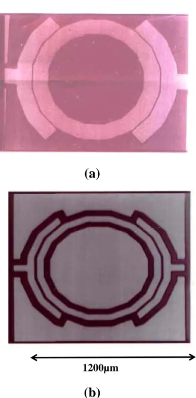
VLSI processing for patterning. The coplanar coupled lines were laid out to form resonators, with the length (λ/2) of the coplanar resonator being dependent on the resonant frequency. For microstrip-type resonators, 2 µm Al was also deposited on the backside of the 200 µm thick Si, as the ground plane. Figures 2.1.2 (a) and (b) are the images of the fabricated CPW and microstrip ring resonators designed at 40 GHz and 30 GHz, respectively. After ring resonator device fabrication, ion implantation of protons was applied to reduce the RF substrate loss. The device RF characteristics
were measured using an HP 8510C Network Analyzer and a probe station to 50 GHz.
2.2.3 Experimental Results
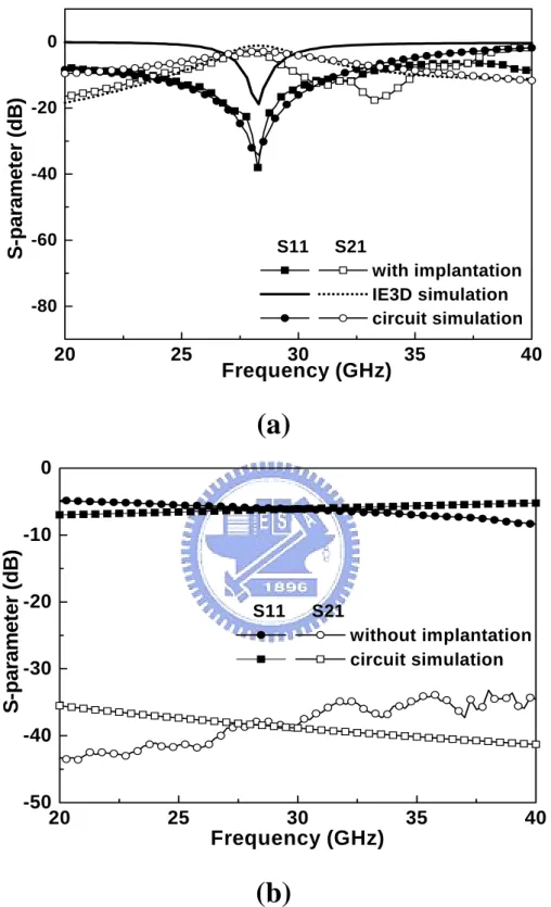
Figures 2.2.1 (a) and (b) present the RF characteristics of CPW ring resonators on VLSI-standard oxide-isolated Si, with and without the ion implantation respectively. For comparison, the IE3D-designed characteristics are also shown in Figure 2(a). The implanted ring resonator has excellent RF performance, with only –1.35 dB S21
insertion loss at the peak transmission of 39.2 GHz and a broad ~13 GHz bandwidth. The small insertion loss is due to the large surrounding stubs being close to the ring that enhance the coupling efficiency. The measured transmission and bandwidth are close to the ring resonator simulation, using IE3D, for an ideal lossless Si substrate. This is the first report of high performance ring resonators on Si substrates at mm-wave regime. The merit of this ion implantation method is the simple process and it being compatible with current VLSI technology. In contrast, the ring resonator device on the same 1.5-µm isolated Si substrate, without ion implantation, shows much worse insertion loss of 15-20 dB over the whole frequency range. Such high loss and poor resonator performance makes the devices unusable.
Figures 2.2.3 (a) and (b) present the RF characteristics of the microstrip ring resonators, shown in Figure 2.2.1 (b), on conventional oxide-isolated Si, with and
without the ion implantation respectively. For comparison, the EM- designed characteristics from an IE3D simulation are also plotted in Figure 3(a). For the ring resonator with ion implantation, good RF performance is achieved with only –3.37 dB S21 insertion loss at the peak transmission of 28.3 GHz and a broad ~6 GHz
bandwidth. This successful microstrip type ring resonator on Si is much more difficult to achieve than the CPW resonator because of the EM field being fully inside the lossy Si substrate. In contrast, the un-implanted microstrip ring resonators show large ~40 dB insertion loss, which prohibits their integration into any RF circuit.
2.3
Modeling and Mechanisms
2.3.1 Analysis from Modeling
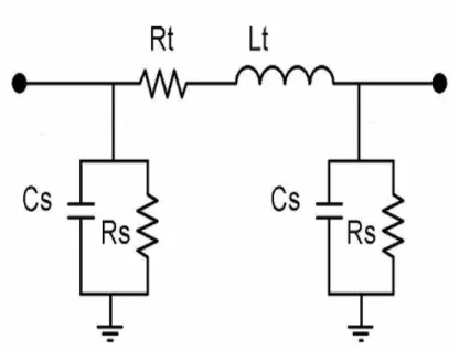
We use the physically-based equivalent circuit model shown in Figure 2.3.1 to simulate the S-parameters. Lt and Rt are the series inductor and parasitic resistor from the long microstrip transmission line body, respectively. The symmetrical Rs and Cs at the input and output ports represent the RF signal loss to the ground plane, which should be large for the bulk microstrip line formed on VLSI-standard low resistivity Si substrate (10 Ω-cm) without ion implantation.
The measured and simulated S-parameters of the bulk and thin-film microstrip transmission lines, with or without implantation, are shown in Figure 2.3.2 (a) and Figure 2.3.2 (b). Good agreement is obtained between the measured and modeled S-parameters, suggesting that the equivalent circuit model in Figure 2.3.3 is appropriated.
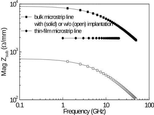
The extracted substrate impedances, deduced from the Rs-Cs sub-circuits for both bulk and thin-film microstrip transmission lines, are shown in Figure 2.3.3. For the bulk microstrip lines on standard Si, the proton implantation can increase the substrate impedance by more than one order of magnitude. For the thin-film microstrip lines, the relatively high substrate impedance arises from the high resistivity SiO dielectric inside the microstrip line body.
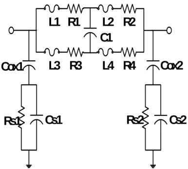
We have also used a physically-based equivalent circuit model, shown in Figure 2.3.4 to simulate the RF characteristics of the ring resonator. The shunt Rs and Cs sub-circuits simulate the substrate loss, and Cox is the parasitic oxide capacitor underneath the resonator of the 1.5 µm SiO2 on the Si substrate. The capacitor C1
represents the gap-coupling capacitor, while the series L and R are the parasitic inductor and resistor from the ring and coupling metal stub. The series LC forms the resonator realized by these coupling lines and the ring body. Figure 2.3.4 shows the equivalent circuit simulated and measured RF characteristics of both the CPW and microstrip ring resonators with ion implantation. Excellent agreement between the measured and simulated S-parameters, shown in Figure 2.3.2 for both CPW and microstrip resonators, was achieved. This indicates the accuracy of the equivalent circuit model. Similar good matching between circuit-simulated and measured S-parameters was also obtained for the resonators without proton implantation in Figure 2.3.2 (b) and Figure 2.3.3 (b). Thus the equivalent circuit can be used to extract the substrate loss from Rs-Cs sub-circuits.
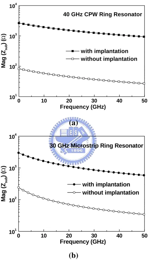
The extracted substrate impedance from the Rs-Cs sub-circuits is shown in Figure 2.3.5. Proton implantation increases the substrate impedances by more than an order of magnitude. The decreasing substrate impedance with increasing frequency is due to the effect of shunt capacitance to ground, which is also consistent with the
higher loss at higher frequency of the transmission line and filter loss in our previous publications.
2.4
Conclusions
We have achieved extremely low power loss for both bulk (0.4 dB/mm at 50 GHz) and thin-film (0.9 dB/mm at 20 GHz) microstrip transmission lines on VLSI-standard Si substrates and fabricated CPW and microstrip ring resonators on Si substrates with good RF performance at ~40 and ~30 GHz, was close to that for ideal IE3D-designed resonators. Proton implantation selectively transforms the low resistivity Si substrates of bulk microstrip transmission line into a high resistivity state. The high performance of thin-film microstrip line results from the high-resistivity SiO2-dielectric being inside the microstrip line body. Both transmission lines can be
integrated into RF circuits and distributed devices at a reduced size compared with using CPW lines. Without implantation such resonators have worse insertion and reflection loss and completely fail. By using equivalent circuit models and EM simulation we conclude that the substrate impedances are the major cause of the poor RF performance.
0 10 20 30 40 50 0 2 4 6 8 10 12 Measured Simulated
bulk microstrip line w/o implanation CPW line w/o implanation
bulk microstrip line with implanation GaAs simulation
Frequency (GHz)
Power Loss (dB/mm)
Fig. 2.1.1 The measured and EM-simulated power loss of 3 mm long bulk microstrip transmission lines. For comparison, results for a 1 mm long CPW line are included. Implantation produces a large loss reduction, from 6.7 dB/mm to 0.4 dB/mm at 50 GHz.
4 8 12 16 20 0 1 2 3 4 5 6 measurement
equivalent circiut simulation IE3D simulation
Power Loss (dB/mm)
Frequency (GHz)
Fig. 2.1.2 The measured and EM-simulated power loss of 0.75 mm long thin-film microstrip transmission lines. The measured loss at 20 GHz is < 1 dB/mm, i.e. much lower than the bulk CPW (3 dB/mm) and microstrip lines (6 dB/mm) in Figure 1 without implantation.
1200µm
(a)
(b)
Fig. 2.2.1Images of fabricated (a) CPW and (b) microstrip ring resonators designed at 40 GHz and 30 GHz, respectively. The long surrounded stubs near the ring are to enhance the coupling efficiency.
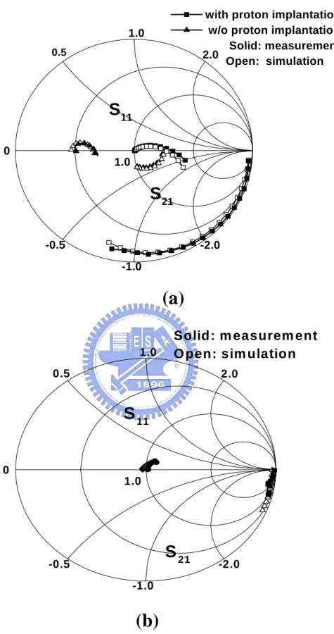
30 35 40 45 50 -70 -60 -50 -40 -30 -20 -10 0 S11 S21 with implantation IE3D simulation circuit simulation S -param et er ( d B ) Frequency (GHz)
(a)
30 35 40 45 50 -40 -30 -20 -10 0 S11 S21 w ithout im plantation circuit sim ulationS -param e te r ( d B) Frequency (G H z)
(b)
Fig. 2.2.2 The measured S-parameters of CPW ring resonators (a) with and (b) without proton implantation. The EM and circuit simulated filter characteristics are shown for reference.
20 25 30 35 40 -80 -60 -40 -20 0 S11 S21 with implantation IE3D simulation circuit simulation S-p a ram e te r ( d B ) Frequency (GHz)
(a)
20 25 30 35 40 -50 -40 -30 -20 -10 0 S11 S21 without implantation circuit simulation S -p a ra m e te r (d B ) Frequency (GHz)(b)
Fig. 2.2.3 The measured S-parameters of 30 GHz microstrip line ring resonators (a) with and (b) without proton implantation. The EM-simulated and the equivalent circuit simulated filter characteristics are also shown for reference. No resonance is observed in (b) due to the substrate loss of ~40 dB.
Fig. 2.3.1 The physically-based equivalent circuit for the microstrip transmission lines. The Lt represents the line inductor, and Rt the parasitic resistor of the transmission line. The substrate loss is modeled by the shunt Rs and Cs to ground.
0.5
S
21S
11with proton implantation w/o proton implantation
Solid: measurement Open: simulation 1.0 -2.0 -1.0 -0.5 2.0 1.0 0
(a)
Solid: m easurem ent O pen: sim ulation
0.5
S
21S
11 1.0 -2.0 -1.0 -0.5 2.0 1.0 0(b)
Fig. 2.3.2 The measured and equivalent-circuit modeled S-parameters of (a) bulk and (b) thin-film microstrip transmission lines on Si substrates. The effect of proton implantation is shown in (a). The different curve lengths are due to different
0.1
1
10
100
10
210
310
4bulk microstrip line
with (solid) or w/o (open) implantation thin-film microstrip line
Mag Z
s ub(
Ω/mm)
Frequency (GHz)
Fig. 2.3.3 The extracted magnitude of the substrate-impedance/mm derived from the bulk and thin-film microstrip transmission lines. The effect of proton implantation is to increase the substrate impedance and thus reduce the loss of the bulk microstrip transmission line.
Cox1
Rs1
R1
R2
R3
R4
L1
L2
L3
L4
Cox2
Cs1
Rs2
Cs2
C1
Fig. 2.3.4 The physically-based equivalent circuit of ring resonators. The L expresses the metal stub, and the C1 is the fringing coupling capacitance of the ring. The
0 10 20 30 40 50 101 102 103 104 Ma g (Z su b ) ( Ω ) with implantation without implantation 40 GHz CPW Ring Resonator Frequency (GHz)
(a)
0 10 20 30 40 50 101 102 103 104Ma
g
(
Z
sub) (
Ω)
with implantation
without implantation
30 GHz Microstrip Ring Resonator
Frequency (GHz)
(b)
Fig. 2.3.5 The extracted magnitude of the substrate impedance from (a) CPW ring resonators and (b) microstrip ring resonators with or without implantation.
Chapter 3
Microwave Filters and Couplers
3.1 Microwave Band-pass Filters on PCB
3.1.1 Motivation
Microstrip ring resonator filters are been widely used in RF front end of a microwave transceiver [3.1.1]. From circuit design point of view, ring resonators have many attractive features, like compact size, low cost, easy fabrication and good out-of-band rejection [3.1.2]. This device has been widely employed and integrated with oscillators, mixers, and antennas. The stepped impedance design [3.1.3]-[3.1.5] can further control the odd- and even-mode resonant frequencies by adjusting geometric parameters of the resonator. This makes ring resonator filters applicable for designing dual-mode bandpass filters with a fractional bandwidth up to 10% [3.1.6]. Due to the need of newly proposed ultra wide band (UWB) specifications, bandpass filters with GHz bandwidth will be required. Microstrip ring resonator filters fabricated on a PCB usually have a relatively small bandwidth. This is mainly due to
chemical etching process and dry etching are about 100 – 150 µm. There are still few papers devoted in investigating microstrip passive devices with coupling gaps less than 100 µm. Previously, we have shown CPW and microstrip ring resonators, broadband and narrow band filters, antenna and transmission lines on ion-implanted Si substrates with excellent RF performance up to 100 GHz [3.1.7]-[2.1.10]. The achievement is partially due to a sufficiently small gap size fabricated on a low RF loss Si substrate generated by ion-implantation by lithography technique. We apply lithography technique to realize a dual-mode ring resonator filter on PCB. The purpose is to make a sufficiently narrow gap between the resonator and feed lines, so that the fractional bandwidth of a dual-mode ring resonator filter can be pushed up to 30%. It is found that the pass band of the fabricated filter has not only good flatness but also a very low insertion loss.
3.1.2 Filter Design and Fabrication
The dual-mode ring resonator shown in Fig. 3.1.1 has two stepped impedance junctions. If there is no impedance junction, the leading two resonances will degenerate into one frequency, and the use of this kind of resonator will be limited. Here, the junctions are symmetric about the skew symmetric plane, the dashed line in Fig. 3.1.1, and make the degenerated resonant frequencies split up into even- and
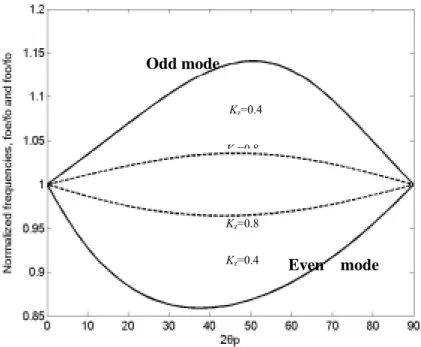
odd-mode resonant frequencies, foe and foo. When the circuit operates in even- and odd-modes, the symmetric plane is an open circuit and grounded plane, respectively. Let the microstrip line section of electrical length of 2θp has a characteristic impedance ZL and the remaining part has ZH. Define an impedance ratio
H L z Z Z K = (1) At respective resonances, the admittance sum of the microstrip sections seen at the impedance junction should be zero. Thus, the resonant frequencies foe and foo can be respectively determined by solving the following transcendental equations:
tan ( ) tan =0 + − p o oe p o oe z f f f f K π θ θ (2) tan tan ( )=0 − + p o oo p o oo z f f f f K θ π θ (3)
Fig. 3.1.2 plots normalized frequencies foo/fo and foe/fo as a function of 2θp. It can be seen that frequencies of the even-mode are always higher than those of the odd-mode when Kz < 1. Also, the smaller the impedance ratio Kz is, the larger separation between the resonant frequencies is. The plots are used to approximate coupling coefficient C12 of the filter:
2 2 2 2 12 oo oe oo oe f f f f C + − = (4)
Note that this coefficient has also to be specified by the formula of filter synthesis: 2 1 12 g g C = ∆ (5)
where g1 and g2 are element values of the low-pass filter prototype and ∆ is the
fractional bandwidth. Thus, for achieving a filter with broad bandwidth, it is important to choose a proper θp with the largest separation between the even- and odd-modes. In our design, θp and Kz are chosen to be 50o and 0.4, respectively.
The second step of the design is to establish proper couplings between the ring resonator and input /output feeding networks. This is important since the passband response will be destroyed due to either over or under coupling. The external quality factor Qe and the fractional bandwidth ∆ are related by
=
∆
0 1g
g
Q
e (6)The coupling capacitance can be found to be 1 1 1 − = e H o Q Z Z Z C π (7)
Where Zo is the system reference impedance. It can be expected that if a large bandwidth is required, the coupling capacitance C can be quite large so that a small coupling gap will be required.
3.1.3. Results and Discussion
Two dual-mode ring resonator filters are designed, fabricated and characterized by an HP 8720C vector network analyzer. The first one has a gap size 240 µm for design a Chebyshev filter with ∆ = 10%, and the other has a gap 40 µm for design a filter with ∆ = 30%. Both filters have a center frequency fc = 1.9 GHz. Figs. 3.1.3 (a) and 3.1.4(b) show the simulated responses.
Figs. 3.1.4(a) and 3.1.4(b) show the measured |S21| and |S11| responses of the
filters with 240 µm and 40 µm, respectively. In Fig.3.1.4 (a), the measured fractional bandwidth is found to be only 9.5%. In the passband, the best insertion return losses are 1.3 dB and -13 dB, respectively. In Fig.3.1.4 (b), the measured fractional bandwidth is 30% which is the same as the simulation. The best in-band insertion and return losses are only 0.50 dB and -17 dB, respectively. It can be observed that the simulation and measured results have a good agreement, which is mainly due to a good process control with small variation. The small coupling gap is the key factor for achieving small insertion loss and broadband characteristics of band-pass filter.
3.1.4 Conclusions
We have fabricated a broadband (30% bandwidth) dual-mode ring resonator filter with a performance closely matching with ideal EM simulation. A small coupling gap realized by using the IC lithography technique, low insertion loss is also obtained. In contrast, the conventional large gap size of the same filter structure has much smaller fractional bandwidth (10%) and larger insertion loss. This technology can be further applied to design microwave passive devices with even smaller coupling gap.
3.2 Microwave Couplers on PCB
3.2.1 Motivation
Directional couplers are important elements in microwave integrated circuits (MIC’s) [3.2.1]. It can be used in design of baluns, power dividers/combiners, filters, attenuators and instrumentation systems. A hybrid coupler, i.e. a coupler with 3-dB coupling, is found useful in building a power distributed amplifier [3.2.2], a balanced mixer [3.2.3], etc. A fully planar conventional microstrip coupler has a coupling less than 10 dB due to lower realizable limit of slot width in microstrip technology. This leads to the development of many methods. In the vertically installed planar (VIP) circuit [3.2.4], coupled lines are constructed perpendicularly to the main microstrip circuit board. In [3.2.5]- [3.2.6], a semi reentrant microstrip section is used to realize the tight coupling. In [3.2.7], couplers are designed in a multilayer structure with two- and three-strip couplings. These approaches rely on the broadside coupling through a dielectric layer between the microstrip lines.
It is also possible to use an original or unfolded Lange coupler for 3 dB coupling. The design concept is based on multifold constructive edge couplings to enhance the coupling capacitance between the two main lines in multiple coupled microstrip. It is found that bond wires are inevitably required in circuit realization, since nonadjacent lines are assumed to have identical potentials.
In this paper, we try to make a conventional single-stage microstrip coupler with a coupling level as high as possible. The high-level coupling is achieved by fabricating a narrow gap between the coupled microstripe using low cost IC process. The design is based on the structure of a 3-dB coupler. Measurement shows that the fabricated coupler has a 4-dB coupling. The measured good results are due to the small coupling gap used in our previous RF passive devices. Note that the entire circuit is fully planar, requires no bond wire, and retrieves the simplicity of the original circuit design.
3.2.2 Filter Design and Fabrication
For a coupler with coupling C, the even and odd mode impedances are required to be [1]
C
C
Z
Z
oe o−
+
=
1
1
(1) C C Z Zoo o + − = 1 1 (2)The Z0 are chosen to be 50 and 42.3 Ω for Device 1 and 2 respectively, where
additional λ/4 converter impedance (Zt) of 46.0 Ω is used for Device 2 to match the
εr = 10.2 and thickness = 1.27 mm is chosen to realize the circuit. The EM simulator IE3D [10] is used to validate the circuit design before the circuit is fabricated. The required line width are 309 µm and 4 µm; the interline spacing are 560 µm and 4 µm for Device 1 and 2, respectively. The circuit is fabricated by conventional low cost IC process with a >1-µm resolution and standard FeCl etching. An infrared red aligner is used for pattern exposure, and HFD5 solution for circuit development. The solution is heated up to 50 – 60 oC to have a better etching in the valley of the central gap.
Circuit measurements are performed by an Agilent/HP 8720C vector network analyzer.
3.2.3 Results and Discussion
Figure 3.2.1(a) shows the photo of the fabricated coupler where an enlarged pattern of a part of the coupled lines is displayed in Figure 3.2.1 (b). Transmission line sections with 50Ω characteristic impedance are used to extend the circuit ports for saving an enough spaces of the SMA connectors for measurement. Since the chemical solution etching is isotropic, the fabricated circuit inevitably has a V-shape coupling gap. From the enlarged circuit picture in Figure 3.2.1 (b), the upper opening of the V-shape gap can be estimated to be 24 µm, since total distance between the outer edges of the strips is 620 µm. The performance of the coupler is simulated by
µm width at valley. Figure 3.2.2 compares the simulated and measured responses of Device 1. In Figure 3.2.2 (a), the measured |S21| (through) and |S31| (coupling)
responses have very good agreement over a frequency range from 3 to 9 GHz. In Figure 2 (b), the isolation and return loss responses of the fabricated coupler are better than 20 dB.
Figure 3.2.3 (a) and 3.2.3 (b) show the measured coupling response, return loss and isolation loss of Device 2, respectively. Good coupler characteristics of high coupling of 3.8 dB, small insertion loss of -3.9 dB and very wide bandwidth (1dB) of 52% are achieved that are comparable to even better than the reported very wide bandwidth data. The slightly inferior return loss of -24.3 dB and directivity of -21.0 dB may be due to small power reflection in non-ideal impedance transformer. The reason of good agreement between measured and modeled coupler characteristics is due to the sharp and accurate etching profile close to EM simulation shown in the insert picture of Figure 3.2.1. However, since the used IC technology is ~2 decades old with only line definition of >1µm, this process may provide simple and low cost solution for fabricating high performance coupler and other RF devices.
Table 3.2.1 summarizes the measured and simulated data of the couplers at 5GHz. The Device 1 has a coupling level (|S31|) of 3.8 dB in simulation and 4.0 dB in
are better than 20 dB, and the 1 dB bandwidth of the circuit is more than 50%. The Device 2 also has a coupling level (|S31|) of 3.8 dB in simulation and 3.9 dB in
measurement. These simultaneously measured high coupling, high directivity, and broad bandwidth are simply due to the smaller coupling gap from the fundamental theory analysis that was justified by the close match between measurements to EM simulations.
3.2.4 Conclusions
A microstrip coupler with a 4-dB coupling level is fabricated on PCB. It is achieved by etching a 14-µm gap. Entire circuit is fully planar and needs no bond wire. This simple technology will have applications to high performance RF passive devices on PCB.
3.3 Conclusions
A fully planar microstrip coupler with a high coupling level up to 4 dB is fabricated on PCB. Based on the conventional coupled-line structure, a gap size of coupled lines about 14 µm is realized by low cost IC process. It has a single stage and requires no bond wire. In measurement, a bandwidth more than 50% and isolation and return loss better than -20 dB are achieved. The measured responses have good agreement with EM simulation data. A high-performance ring resonator filter is fabricated on PCB with aid of the IC lithography technique. The filter, designed at 1.9 GHz, has a very large fractional bandwidth (up to 30%), an insertion loss of 0.50 dB, a flat |S21| response in pass-band, a
return loss better than ~30 dB at two transmission poles and a rejection level of –40 dB at attenuation poles. In addition, the measured characteristics are very close to ideal design by EM simulation. The achieved excellent broadband device characteristics are due to a small coupling gap in the filter. In contrast, the conventional method can only have a large coupling gap with relatively small bandwidths and relatively large insertion losses. The excellent device performance reflects that this technique makes the ring resonator filter applicable from narrow band to broadband designs.
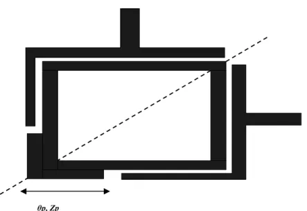
Fig. 3.1.1 Structure of a dual-mode ring resonator filter θp, Zp
Fig. 3.1.2 Normalized frequencies foe/fo and foe/fo as a function of electrical length 2θp Odd mode Even mode Kz=0.4 Kz=0.8 Kz=0.4 K =0 8
1.0 1.5 2.0 2.5 3.0 -50 -40 -30 -20 -10 0 S11, S21 (dB) Frquency (GHz) simulated s11 simulated s21 240 µm coupling gap (a) 1.0 1.5 2.0 2.5 3.0 -50 -40 -30 -20 -10 0 S11, S21 (dB) Frquency (GHz) simulated s11 simulated s21 40 µm coupling gap (b)
Fig. 3.1.3 Simulated responses of the dual-mode ring resonator filter with center frequency fc = 1.9 GHz. (a) Coupled gap = 240 µm, ∆ = 10%. (b) Coupling gap = 40 µm, ∆ = 30%.
1.0 1.5 2.0 2.5 3.0 -50 -40 -30 -20 -10 0 S11, S21 (dB ) Frquency (GHz) measured s11 measured s21 240 µm coupling gap (a) 1.0 1.5 2.0 2.5 3.0 -50 -40 -30 -20 -10 0 S11, S21 (dB) Frquency (GHz) measured s11 measured s21 40 µm coupling gap (b)
Fig. 3.1.4 responses of the dual-mode ring resonator filter with center frequency fc = 1.9 GHz. (a) Coupled gap = 240 µm, ∆ = 10%. (b) Coupling gap = 40 µm, ∆ = 30%.
(a)
(b)
Fig. 3.2.1 The fabricated coupler. (a) Photo of the entire circuit. (b) Enlarged picture of the coupled lines.
31 21 |S |, |S | (d B) 21 Simulated |S | 21 Measured |S | 31 Simulated |S | 31 Measured |S | 0 -10 -20 -30 -40 Frequency(GHz) 10 9 8 7 6 5 4 3 2 1 (a) |S |, |S | (dB) 11 41 11 41 11 Simulated |S | Measured |S | Simulated |S | 10 8 7 9 6 5 4 2 3 Frequency(GHz) Measured |S |41 0 -10 -20 -40 -30 1 -50 (b)
Fig. 3.2.2 The measured and simulated responses of the fabricated Device 1. (a) |S21|
-40 1 -30 -20 -10 Measured |S | Frequency(GHz) 5 2 3 4 6 7 8 31 Simulated |S | Measured |S | Simulated |S | 21 21 31 0 10 9 31 21 |S |, |S | (dB) (a) Simulated |S | Simulated |S | -40 -50 1 2 -30 -10 -20 0 Frequency(GHz) 3 4 5 6 7 8 9 10 41 Measured |S |41 Measured |S | 11 11 |S |, |S | (dB) 11 41 (b)
Fig. 3.2.3 The measured and simulated responses of the fabricated Device 2. (a) |S21|
Device1 Simulated Measured S11(dB) S21(dB) S31(dB) S41(dB) 1 dB BW (GHz) -28.2 -3.07 -3.82 -30.0 3.1-6.0 58% -26.9 -2.91 -4.02 -21.0 3.4-6.0 52%
Device2 Simulated Measured
S11(dB) S21(dB) S31(dB) S41(dB) 1 dB BW (GHz) -35.4 -2.90 -3.90 -29.8 3.3-6.2 58% -24.3 -2.90 -3.80 -21.0 3.7-6.3 52%
Chapter 4
Coupling and Dynamic Power
Losses in VLSI Interconnects
4.1. AC Power Loss and Signal Coupling
4.1.1 Motivation
The down-scaling of silicon device technology into the sub-100nm regime results in the static and dynamic power consumption becoming a major impediment for high-performance integrated circuits (ICs). The importance of the dynamic power consumption issue has been prominent recently [4.1.1]-[4.1.2], because the dynamic power loss is an even more difficult challenge than for the DC power case [4.1.1]-[4.1.4]. The latter can be reduced by using a high-κ gate dielectric and alternative device designs, such as FinFETs. The dynamic power at high frequency (f) mainly arises from the parasitic capacitance (C) of both the MOSFETs and the backend interconnects, and is essentially described by the term Cv2f/2, where the v is
concern of dynamic power loss in the interconnects can be reduced by using Si-on-Insulator (SOI) [4.1.2], [4.1.5]. The trend in high performance ICs, such as microprocessors and communication ICs, is towards higher operation frequencies and interconnect densities which exacerbate the problem.
Recently we proposed and demonstrated a three-dimensional (3D) VLSI integration structure to address this issue, by using shorter interconnects [4.1.4]. Here we report measurements of the dynamic power loss and also the coupling loss in VLSI backend interconnects. We found good agreement between Electro-Magnetic (EM) simulations and the data, supporting our previous conclusions [4.1.4]. The integration scheme yields shorter interconnects and helps reduce both the coupling and dynamic power losses for high density and closely-spaced interconnect lines.
4.1.2 Experimental Procedure
To imitate the parasitic loss in the interconnects, such as those shown schematically in Fig. 4.1.1. The two long parallel lines with lengths of 0.25, 0.5 and 1 mm and with different line-spacings of 2, 5, and 10 µm are depicted in Fig. 4.1.1(b). The 3D integration [4.1.3]-[4.1.4] can reduce parasitic effects of the interconnects by as much as a half or ¼, by folding the 2D IC once or twice. Different inter-metal dielectric (IMD) thickness of 0.7 or 6 µm were used to simulate the local or global
interconnects using metal-1 (M1) or metal-6 (M6) layers of the 1-Poly-6-Metal (1P6M) structures shown in Fig. 4.1.1(a). Figs. 4.1.2(a) and 4.1.2(b) show the images of fabricated parallel lines, where additional co-planar waveguide (CPW) structure and 150 µm spacing GSG probing pads were used to study the power loss and signal coupling loss. The CPW transmission lines were fabricated using 2 µm thick Al metal on PECVD deposited IMD SiO2 above the Si substrate. The RF power loss
(1-|S21|2-|S11|2) was directly obtained from the S-parameters measured with an 8510C
network analyzer [4.1.6]-[4.1.9]. This approach was necessary due to the open and shorts being non-ideal in the RF regime. The EM method avoids using complicated equivalent circuit models that can be difficult to solve for the intricate interconnects [4], which are distributed. For comparison we also studied the dynamic power loss and coupling of parallel lines on high-resistivity Si (HRS) substrates [4.1.10]-[4.1.11] which had a resistivity of 1.5×10⁴ Ω-cm
4.2 1-Poly-1-Metal 0.18-
µm Si MOSFETs
4.2.1 Experimental Results and Discussion
Figures 4.2.1(a), 4.2.1(b) and 4.2.1(c) show the simulated and measured S21, S11
and dynamic power loss, respectively, of 1 mm and 0.25 mm long parallel M1 lines with 2 µm gap widths. The M1 lines with 0.7 µm IMD SiO2 imitate the local
interconnects in VLSI ICs. There is good agreement between the measured S21
coupling, S11 and power loss with the simulation data, suggesting that the 3D EM
simulation is valid. Such good matching is difficult to achieve using an equivalent circuit model with discrete elements, due to the complicated parasitics and distributed circuit effects that must be accounted for. The S21 coupling increases with increasing
frequency resulting in signal loss in the parent transmission line and creates signal disturbances (cross-talk) in nearby lines. The power loss also increases with increasing frequency which is an important issue for future high performance circuits. We define the maximum operation frequency of an IC to be where either the power or signal coupling loss is 3 dB. Then the maximum operation frequency is limited to 3 GHz by the power loss if 1 mm long local M1 parallel lines are used. This can be increased to 20 GHz by using shorter parallel interconnect lines of 0.25 mm in length. Thus the performance of high frequency ICs is limited by the total length of local interconnects, and by the line spacing to other interconnection lines. One method to
overcome this problem is to use higher resistivity substrates, compared with VLSI-standard 10 Ω-cm resistivity ones. The power loss improves significantly for the same parallel lines on HRS substrates. This is due to the reduced power loss in the parasitic substrate RC networks [7], [9]. This power loss reduction comes at the cost of increased S21 coupling, so that the maximum operation frequency is limited to ~16
GHz by the 3 dB coupling loss of 1 mm long M1 lines. Decreasing the line length from 1 mm to 0.25 mm is the most effective way to reduce both the coupling and dynamic power losses and can be achieved by a 3D integration scheme shown in Fig. 1(b).
We also measured structures that had the (M1) line spacing increased to 10 µm. Good agreements between the measurements and the EM simulation was also obtained, with data similar in functional form to those shown in Fig. 3. Table 1 details the values of the parameters for various structures, at 20 GHz. Increasing the line spacing from 2 to 10 µm improves the coupling loss slightly but the improvement at the cost of a reduction of the interconnect density. By using HRS the dynamic power loss can be reduced but the coupling loss unfortunately increases. This suggests that the best way to reduce both coupling and dynamic power losses in high density interconnects is to use shorter interconnect lengths, as provided by 3D integration and HRS substrates.
4.3 1-Poly-6-Metal 0.18-
µm Si MOSFETs
4.3.1 Experimental Results and Discussion
We have also investigated the coupling and power losses of global interconnect lines using M6. Figures 4.3.1(a), (b) and (c) show the simulated and measured S21, S11
and dynamic power loss, respectively, of 1 mm and 0.25 mm long parallel M6 lines with a 2 µm gap width. Since the parallel lines have 6 µm thick SiO2 isolation above
the Si substrate, the power loss was significantly reduced, compared with those for the 0.7 µm SiO2 case. The coupling loss was only slightly improved due to the strong
gap-width dependence of the lateral EM field. This confirms the importance of reducing the interconnect line length by 3D integration.
4.3.2 Signal Coupling Loss and Power Loss
Figures 4.3.2(a) and 4.3.2(b) show the measured signal coupling loss and dynamic power loss, respectively, with different line length, gap width, and substrate resistivity dependences. Only M1 local interconnects were studied since the losses are more severe than those using M6. The signal coupling loss improves with increasing gap spacing from 2 µm to 10 µm; however this in conflict with the increased interconnect density provide by down-scaling.