in 40-nm digital bulk CMOS technology. The theoretical max-imum voltage gain that an amplifier can achieve and the loss of a matching network are derived for the optimization of a few hundred gigahertz amplifiers. Accordingly, the bias and size of transistors, circuit topology, and inter-stage coupling method can be determined methodically to maximize the amplifier gain. The measured results show that the amplifier exhibits a peak power gain of 10.5 dB at 213.5 GHz and an estimated 3-dB bandwidth of 13 GHz. The power consumption is only 42.3 mW under a 0.8-V supply. To the best of the authors’ knowledge, this work demon-strates the CMOS amplifier with highest operation frequency reported thus far.
Index Terms—Amplifier, maximum gain, shunt stub matching, transmission line.
I. INTRODUCTION
A
PPLICATIONS beyond 200 GHz, aiming at the broad bandwidth for communication and the penetration capa-bilities for object detection, have drawn great attention recently [1], [2]. These wireless systems need high integration tech-nology to achieve mobile, reliable, and economic production. Advanced digital CMOS technologies offer a promising oppor-tunity to meet the requirements at such high frequencies. With continuous device scaling, the transistor speed is fast enough that circuits working near and even beyond 200 GHz become feasible, such as frequency dividers [3], [4], oscillators [5]–[7], and amplifiers [8]–[10].Among the circuits, the amplifier is very critical to provide gain and improve system sensitivity. Yet amplifier design above Manuscript received April 18, 2013; accepted April 23, 2013. Date of pub-lication May 14, 2013; date of current version May 31, 2013. This work was supported by the National Science Council, Taiwan, under Grant NSC 101-2220-E-009-013 and Grant 101-2220-E-009-053, by the Ministry of Ed-ucation in Taiwan under the Aiming for the Top University (ATU) program, and by MediaTek Inc. under a fellowship.
C.-L. Ko is with the Department of Electronic Engineering and the Institute of Electronics, National Chiao Tung University, Hsinchu 300, Taiwan, and is also with the National Chip Implementation Center (CIC), National Applied Research Laboratories, Hsinchu 300, Taiwan (e-mail: [email protected]).
C.-H. Li and C.-N. Kuo are with the Department of Electronic Engineering and the Institute of Electronics, National Chiao Tung University, Hsinchu 300, Taiwan (e-mail: [email protected]).
M.-C. Kuo is with the Information and Communications Research Labo-ratories (ICL), Industrial Technology Research Institute (ITRI), Hsinchu 310, Taiwan.
D.-C. Chang is with the National Chip Implementation Center (CIC), Na-tional Applied Research Laboratories, Hsinchu 300, Taiwan.
Color versions of one or more of the figures in this paper are available online at http://ieeexplore.ieee.org.
Digital Object Identifier 10.1109/TMTT.2013.2260767
lenges. Firstly, the unity current gain frequency is lim-ited. For instance, is only around 300 GHz in 40-nm dig-ital CMOS. As the operation frequency gets close to , the transistor gain becomes relatively low. Although device scaling can improve , it indeed lowers the output resistance, which is unfavorable for the amplifier gain. This explains why there exists debate if advanced technologies are really beneficial for RF, and even terahertz, circuit designs. Secondly, passive com-ponents have a low quality factor ( ) because of a lossy silicon substrate. The condition is worse in digital processes for lack of an ultra-thick metal layer and high performance metal–in-sulator–metal (MIM) capacitors. Low passive components cause significant signal loss in impedance matching networks. Another issue is that the supply voltage scales down with the technology, making circuit design more challenging. All these issues need to be considered carefully to have a high-gain am-plifier in an advanced digital CMOS process.
Many prior studies presented amplifiers operating beyond 100 GHz in CMOS technologies [8]–[20]. The common-source (CS) or cascode topologies are commonly seen for signal amplification. However, the aforementioned circuits lack of a design methodology to deal with the issues of low-gain tran-sistors and low- passive components. The passive loss issue confuses designers in transistor sizing, e.g., in [21]. Previous study of the design algorithm [22] is not easy to include the passive loss and select device size. In this paper, the amplifier design is developed based on the maximum voltage gain of an amplifier and the insertion loss (IL) of an impedance transfor-mation network. With the design methodology, the bias, device size, circuit topology, and inter-stage coupling method can be optimized to achieve the maximal gain near .
This paper is organized as follows. In Section II, the design methodology for the 210-GHz amplifier is presented. The an-alytical formulas of the maximum achievable voltage gain and the IL of a matching network are derived. Section III presents the implementation of a 210-GHz CMOS amplifier in 40-nm digital CMOS technology. The experimental results are shown in Section IV. Finally, Section V concludes this work.
II. AMPLIFIERDESIGNMETHODOLOGY
An amplifier can offer a maximum available power gain (MAG) related to its -parameters [23]. Researchers used to design amplifiers based on MAG. The design, however, lacks of the information how to select circuit topology and choose transistor size. This paper is aimed to obtain the design guideline for amplifier design at frequencies close to . It will be shown that the passive matching network reduces amplifier 0018-9480/$31.00 © 2013 IEEE
Fig. 1. Equivalent-circuit model of a narrowband amplifier.
gain significantly although the active device is still capable of providing good gain.
A. Maximum Achievable Voltage Gain
Unilateral amplifier design can serve as the design guideline for maximum gain. The unilateral assumption is often found ac-ceptable when the error is less than 0.5 dB or so. A unilateral narrowband amplifier can be modeled by the equivalent circuit, as illustrated in Fig. 1. Instead of using -parameters, it is easier to obtain design insight by modeling the input and output im-pedances of the active device as and in series and and in parallel, respectively. The transconductance of the active device is designated as .
According to the unilateral model in Fig. 1, the maximum voltage gain under lossless matching network can be derived as (1) where is the frequency of interest and is approximated as . Similar analysis is also given in [24] and [25], but the input impedance is not taken into consideration, which might lead to errors in evaluating the active device gain. When
, (1) can be further simplified as
(2) Fig. 2 shows of a 40-nm nMOS transistor, together with MAG and the current gain for comparison. The tran-sistor width is 10.8 m. The gate-to-source voltage and the supply voltage are both set to 0.8 V. As can be observed, derived using the unilateral model matches MAG very well within the unconditionally stable region, which is the fre-quency band of interest in this work. This shows that unilateral design is suitable.
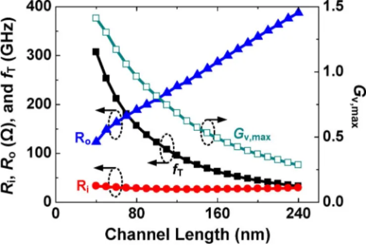
Consequently, can be used as a guideline to design millimeter-wave amplifiers at 210 GHz, although only analog parameters appears in (2). The equation indicates that high and can increase amplifier gain. From the device viewpoint, a long channel length benefits the former, but jeopardizes the latter. To the first-order effect, device characteristics give
and , which, in turn, yields to . Obviously, advanced technologies are still preferred. This is dif-ferent from the analog circuit design using large intrinsic gain,
Fig. 2. Simulated MAG, , and current gain of a 40-nm nMOS transistor.
Fig. 3. Simulated , , , and of a 40-nm nMOS transistor at 210 GHz.
which might be actually lower in advanced technologies. Fig. 3 shows the simulated parameters extracted from the -parame-ters of a 40-nm nMOS transistor, as that in Fig. 2 if the channel length is varied. Smaller gives a larger gain. When ap-proaches to , a proper resistance ratio of can still en-sure a good gain level.
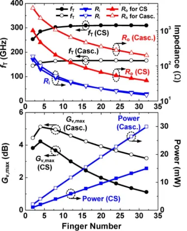
From the circuit viewpoint, the topology of a high is advantageous, such as the cascode. As compared to the CS, the gain boost is roughly by a factor of , where represents the transistor intrinsic gain. The intrinsic gain actu-ally decreases in very advanced technologies so that the advan-tage becomes less effective. The comparison is shown in Fig. 4 by sweeping the finger number. is set at 0.8 V for tran-sistors. is 0.8 V and 1.6 V for the CS and cascode, re-spectively. is about the same in both cases and decreases as the finger number increases. The cascode topology exhibits a larger impedance ratio, about five times larger than that of the CS. Yet its is lower due to the parasitic capacitance between the CS and common-gate transistors. Accordingly, the cascode topology shows a maximum gain around 1 dB higher at the finger number of 4. Nevertheless, the power dissipation is twice that of the CS. Actually, it will be shown later that the cascode no longer has a higher gain than that of the CS once the IL of
Fig. 4. Simulated , , , , and power consumption of CS and cascode (Casc.) topologies at 210 GHz.
matching network is considered. The details will be discussed as follows.
B. IL of Matching Network
The IL of the matching network inevitably decreases the am-plifier gain. It is valuable to assess how the network loss affects amplifier design. Instead of the common simple L-section net-works and transformers [26], the shunt stub of transmission lines used in other designs beyond 200 GHz [23], [24] is chosen as the matching network in this work to eliminate the issue of lim-ited self-resonant frequency.
To analyze the IL, we consider the impedance transformation from arbitrary load impedance of to a source impedance of , as illustrated on a Smith chart in Fig. 5(a) for . The shunt-stub matching network comprises two lossy trans-mission lines of and with length and , respec-tively, as shown in Fig. 5(b). Both lines are with a characteristic impedance of . Either path through A or B can be selected. As far as the loss is concerned, a shorter path is always better.
Let the line loss be dB/ . The IL is characterized by the
ratio of , given by
(4)
Fig. 5. (a) Smith chart of impedance matching. (b) Shunt-stub matching circuit.
Fig. 6. IL of the shunt-stub matching network.
Fig. 7. Calculated , , and total gain of CS and cascode (Casc.) topolo-gies at 210 GHz.
where and are the real parts of the two admittance
and , respectively, and is the
load reflection coefficient referring to . The length of and can be acquired from fulfilling the input complex conjugate matching condition [29].
Given equal to 50 , the calculated and the simulated re-sults of the IL at 210 GHz are as shown in Fig. 6. The line loss is assumed 2.8 dB/ , taking from the transmission line de-signed in Section III(a). In general, and could be com-plex values. In the analysis, is assumed to be real, and is 50 . The simulation is conducted using the transmission line
Fig. 8. Schematic of the proposed amplifier.
Fig. 9. Measured and modeling losses of the microstrip lines.
Fig. 10. Simulated versus current density .
model in the Agilent Advanced Design System (ADS). The re-sults confirm that IL can be reduced if is close to . In other words, IL is larger if the impedance transformation ratio is higher. A similar conclusion with different types of matching networks can be found in [26].
This raises an issue of the tradeoff between and IL. A large calls for a large ratio of , which, in turn, requires a large impedance transformation ratio in the matching networks and leads to a high IL. This is especially serious at a few hundred gigahertz because IL can significantly deteriorate
Fig. 11. Simulated versus power consumption for a single stage.
Fig. 12. Cross-section view of the MOM capacitors formed by dummy metals for the ac bypass at the power node, and the connection to the signal line and the ground of the microstrip line.
the low active gain. An optimal ratio of is therefore nec-essary, which can be achieved by the selection of proper tran-sistor size.
ILs are added to the analysis to obtain the total am-plifier gain. The better circuit topology and the optimal tran-sistor size can then be determined. The IL of the input matching network is due to impedance transformation from to 50 , and the IL of the output matching network from to 50 , where and are the input and output impedance of the active circuits. Fig. 7 shows the total ampli-fier gain as the finger number is varied from 2 to 32, with per
Fig. 13. Inter-stage matching topology and IL as the short stub is near the: (a) previous stage and (b) present stage.
finger width of 0.9 m. The bias condition is the same as that in Fig. 4. The of the cascode topology is the worst because of a high-impedance transformation ratio. This greatly reduces the total gain of the cascode topology. It turns out that both circuits give similar total gain around 1.5 dB with an optimal finger number of 12 and 20 for the CS and cascode, respectively. Note that the current dissipation is proportional to the finger number. The cascode topology consumes more current together with a higher supply voltage. Evidently, the CS topology shall be chosen to make the best tradeoff among the realized gain, supply voltage, and power consumption.
III. 210-GHz AMPLIFIERDESIGN
Fig. 8 shows the proposed 210-GHz amplifier using a 40-nm digital CMOS process. Multiple CS amplifiers are cascaded without inter-stage coupling capacitors. Based on the above discussion, the finger number of the transistor is chosen as 12 to have the maximum total gain. The shunt-stub matching network is applied to the input and output matching networks. Eventually the inter-stage matching is realized by a single short stub. Moreover, the number of cascaded stages is designed to be nine to achieve sufficient gain. The details will be presented as follows.
A. Microstrip Line Design
The planar types of coplanar waveguides and microstrip lines are commonly chosen in on-chip implementation. The microstrip line is adopted in this work because of the struc-ture simplicity and better ground accessibility to reduce the connecting loss to the ground. Besides, its ground plane also shields the lines from the lossy substrate to reduce the line loss. The top copper metal is used as the signal line. The two bottom
metal layers, M1 and M2, are connected together by vias as the ground plane. Note that opening slots are required on the ground plane to meet the metal density rule in chip fabrication. The slots are placed on M1 and M2 in a complementary manner to reduce the field penetration into the lossy substrate.
The microstrip lines are used to match the input and the output impedance of an nMOS transistor to 50 . The line width is chosen as 4.5 m in this circuit. The measured line loss using two network analyzer systems for the frequency bands of 0.01–67 and 140–220 GHz is shown in Fig. 9. The multi-line de-embedding method is used to remove the pad effects with two lines of 720- and 540- m long [30]. However, the de-embedded results are still affected by the line resonance at high frequencies so that there exists ripples in the measured data over the frequency range of 140–220 GHz. The microstrip line is also modeled using the MLIN model in ADS by the approach in [31]. The measured loss is 2.8 dB/ at 210 GHz, where is around 750 m for the microstrip line at 210 GHz. The data is comparable to the reported results, around 2.5 to 6.7 dB/ at 110 GHz [32]–[36] and 2.2 dB/ at 200 GHz [9] in bulk CMOS technologies. The measured is around 55 at 210 GHz.
B. Bias Optimization
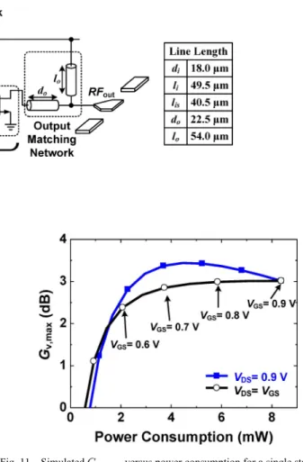
The transistor shall be biased at a proper current density for maximum [37]. Fig. 10 shows versus the current density. Two cases are included, one with a fixed of 0.9 V, and the other with equal to . The differences in and the corresponding optimal current densities are negligible, meaning that is insensitive to variation. Actually the latter case benefits in inter-stage connection as far as direct dc coupling is concerned. Hence, the current density of 0.67 mA/ m is chosen in this work.
Fig. 14. Chip micrograph of the 210-GHz amplifier.
Fig. 15. Measured (symbols) and simulated (solid lines) -parameters and noise figure of the 210-GHz amplifier.
C. Inter-Stage Design
In the multi-stage amplifier design, the inter-stage connection can be realized either by ac or dc coupling. Although ac coupling allows each stage to have independent gate bias voltage for the optimal gain, it causes extra signal loss induced by the dc block capacitor.
Fig. 11 shows of a single-stage CS amplifier. Given the same power consumption, the case with an independent gate bias gives larger by 0.45 dB, as compared to the case of . However, a metal–oxide–metal (MOM) capacitor for dc blocking induces over 1-dB loss at 210 GHz based on the simulation. It is obvious that dc coupling is preferred to alleviate gain degradation.
Keeping the dc voltage node well ac grounded for single-ended circuits is essential to reduce parasitic effects. This work adopts decoupling capacitors for ac grounding, which are formed by the metal layers distributed on the entire chip, as shown in Fig. 12. Odd and even metal layers are connected to the power and ground, respectively. The layers are connected to one another by vias through the holes in the
Fig. 17. Measured output power, gain, and PAE of the 210-GHz amplifier.
Fig. 18. Measured and calculated gain of the 210-GHz amplifier.
adjacent layers. This can maximize the capacitance between and the ground and also reduce the parasitic effects of the needed interconnects between the pads and circuits.
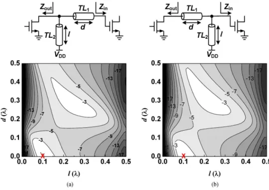
The inter-stage connection is implemented by the shunt-stub matching network from to directly. Generally, shorter transmission lines are better. Two possible configurations are illustrated as shown in Fig. 13. In each one, two solution sets of transmission-line lengths can be found to meet the matching condition. The contour plots of the network IL provide more in-formation over the ranges with and . From the plots, the optimal length of and for the minimum loss, marked as anX, can be determined as zero and , re-spectively, for both cases. This concludes that the inter-stage matching can be reduced to a single shunt stub. The loss is only 0.94 dB at 210 GHz.
D. Layout Consideration
The circuit layout needs to be carefully arranged to reduce undesired parasitic effects. Fig. 14 shows the chip micrograph of the fabricated amplifier. For coupling reduction, the shunt stubs for the inter-stage matching are placed in the upper position for the odd stages and in the lower position for the even stages. In this way, the currents of the adjacent stubs have the same phase, and the magnetic field coupling increases the inductance. This helps to reduce the required line length and the loss can be further minimized. Note that the amplifier with this layout style is checked and shows no stability issue.
The signal pads with the dimension of 40 m 40 m are ta-pered to reduce the step discontinuity. Two bottom metal layers are used as ground shielding from the substrate. The power pads for dc bias are placed 200 m away from the signal pads to avoid probe collision. All areas, except pads and active areas, are used to form the MOM capacitors between and the ground. They also act as the dummy metals to fulfill the density rule. The entire chip occupies the area of 450 m 270 m, while the core circuit only 103 m 130 m.
Agilent ADS Momentum is used to conduct the post-layout simulation. The layout parasitic increases and to be 1.0 and 0.9 dB, respectively, and each inter-stage matching loss to 1.6 dB. The simulated gain of each stage has 3.0 dB at 210 GHz when and are 0.8 V. To have the gain larger than 10 dB with a margin, a stage number of 9 is selected. The total gain of the nine-stage amplifier is 12.3 dB at 210 GHz, which in-cludes the losses of the input, the output, and the eight inter-stage matching networks. The simulated power consumption is only 52.6 mW.
IV. MEASUREMENTRESULTS
The proposed amplifier is implemented using TSMC 40-nm digital CMOS technology where MIM capacitors and ultra-thick top metal are not available.
The amplifier is measured on chip using a network analyzer system that can support measurement from 140 to 220 GHz. The system consists of a dc subsystem HP 4142B and an RF
subsystem Agilent E8361C with millimeter head controller, N5260A, and millimeter-wave test head module, N5256AW05. The calibration by line–reflect–reflect–match (LRRM) is ap-plied to move the reference planes to the probe tips. After calibration, the line standard shows that and
are all smaller than 40 dB, and is 0.02 with 0.02-dB variation. The match standard has and of 25 dB with 5-dB variation. The input power level at the probe tip is fixed at 25 dBm.
Fig. 15 presents the measured -parameters. The measured peak is 10.5 dB at 213.5 GHz. The gain remains 9.3 dB at 220 GHz. If the upper 3-dB frequency is symmetric with respect to the peak gain frequency, the 3-dB bandwidth can be estimated as 13 GHz. and are 12 and 22 dB at 213.5 GHz, re-spectively. The reverse isolation, , is below 30 dB, which confirms that the amplifier is unconditionally stable. The ampli-fier consumes only 52.9-mA dc current under a 0.8-V supply. Limited by experimental equipment, the noise figure (NF) is only available by simulation. As shown in Fig. 15, the NF is 13.4 dB at 210 GHz.
Linearity performance is measured by the customized setup in Fig. 16. The system contains a signal source, a power ampli-fier, 2 and 3 multipliers, an attenuator, a probe station with ground–signal–ground (GSG) probes, and the power meter. The output power is measured by directly connecting output of the attenuator to a power meter. The device-under-test (DUT) is tested using on-wafer GSG probes. The power at the probe tip is calibrated with the measured loss of each probe. Fig. 17 shows input power sweep results at 0.8-V power supply and signal source of 35.583 GHz. Output 1-dB gain compression point dB is at 7.2 dBm. The saturated output power is 3.2 dBm when gain drops to 0 dB. The peak power-added efficiency (PAE) is around 0.75%. At V, increases to
2.4 dBm.
The measured results under different supply voltages are also examined as shown in Fig. 18 along with the associated power consumption. The calculation results are also included for com-parison. The trend of calculation and measurement results is
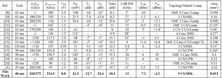
100 GHz. Clearly, the proposed amplifier presents the highest operating frequency while using the lowest supply voltage and the smallest chip area.
V. CONCLUSION
A 210-GHz amplifier is successfully designed and verified in 40-nm digital CMOS technology. The measured results show the peak power gain of 10.5 dB at 213.5 GHz. The power con-sumption is only 42.3 mW under a 0.8-V supply. The occu-pied chip area is only 0.013 mm . The agreement between the measured and the simulated results verifies the proposed design approach.
ACKNOWLEDGMENT
The authors would like to acknowledge the Taiwan Semicon-ductor Manufacturing Company (TSMC), Hsinchu, Taiwan, for technology providing and chip fabrication, National Device Laboratories (NDL), Hsinchu, Taiwan, for the measurement support, and ANSYS, Taipei, Taiwan, for design tool support.
REFERENCES
[1] B. Cetinoneri, Y. A. Atesal, A. Fung, and G. M. Rebeiz, “ -band am-plifiers with 6-dB noise figure and milliwatt-level 170–200-GHz dou-blers in 45-nm CMOS,” IEEE Trans. Microw. Theory Techn., vol. 60, no. 3, pp. 692–701, Mar. 2012.
[2] I. Kallfass, A. Tessmann, H. Massler, A. Leuther, M. Schlechtweg, and O. Ambacher, “A 200 GHz active heterodyne receiver MMIC with low sub-harmonic LO power requirements for imaging frontends,” in Proc. Eur. Microw. Conf., 2009, pp. 45–48.
[3] Q. J. Gu, H.-Y. Jian, Z. Xu, Y.-C. Wu, F. Chang, Y. Baeyens, and Y.-K. Chen, “200 GHz CMOS prescalers with extended dividing range via time-interleaved dual injection locking,” in Proc. IEEE RFIC Symp., May 2010, pp. 69–72.
[4] I. T. Lee, C. H. Wang, B. Y. Lin, and S. I. Liu, “258.16–259.95 GHz injection-locked frequency divider,” IET Electron. Lett., vol. 46, no. 21, pp. 1438–1439, Oct. 2010.
[5] Y. M. Tousi, O. Momeni, and E. Afshari, “A 283-to-296 GHz VCO with 0.76 mW peak output power in 65 nm CMOS,” in IEEE Int. Solid-State Circuits Conf., 2012, pp. 258–259.
[6] D. Shim, D. Koukis, D. J. Arenas, D. B. Tanner, E. Seok, J. E. Brewer, and K. K. O. , “Components for generating and phase locking 390-GHz signal in 45-nm CMOS,” in IEEE VLSI Circuits Tech. Symp. Dig, 2012, pp. 10–11.
[7] B. Razavi, “A 300-GHz fundamental oscillator in 65-nm CMOS tech-nology,” IEEE J. Solid-State Circuits, vol. 46, no. 4, pp. 894–903, Apr. 2011.
[8] Z. Xu, Q. J. Gu, and M.-C. F. Chang, “200 GHz CMOS amplifier working close to device ,” Electron. Lett., vol. 47, no. 11, pp. 639–641, May 2011.
[9] M. Seo, B. Jagannathan, J. Pekarik, and M. J. W. Rodwell, “A 150 GHz amplifier with 8 dB gain and 6 dBm in digital 65 nm CMOS using dummy-prefilled microstrip lines,” IEEE J. Solid-State Circuits, vol. 44, no. 12, pp. 3410–3421, Dec. 2009.
[13] R. Fujimoto, M. Motoyoshi, K. Takano, and M. Fujishima, “A 120 GHz/140 GHz dual-channel ASK receiver using standard 65 nm CMOS technology,” in Proc. Eur. Microw. Conf., 2011, pp. 628–631. [14] D.-R. Lu, Y.-C. Hsu, J.-C. Kao, J.-J. Kuo, D.-C. Niu, and K.-Y. Lin, “A 75.5-to-120.5-GHz, high-gain CMOS low-noise amplifier,” in IEEE MTT-S Int. Microw. Symp. Dig., 2012, pp. 910–912.
[15] Q. J. Gu, Z. Xu, and M.-C. F. Chang, “Two-way current-combining -band power amplifier in 65-nm CMOS,” IEEE Trans. Microw. Theory Techn., vol. 60, no. 5, pp. 1365–1374, May 2012.
[16] O. Momeni and E. Afshari, “A high gain 107 GHz amplifier in 130 nm CMOS,” in Proc. IEEE Custom Integr. Circuits Conf., Sep. 2011, pp. 1–4.
[17] B. Heydari, M. Bohsali, E. Adabi, and A. M. Niknejad, “Millimeter-wave devices and circuit blocks up to 104 GHz in 90 nm CMOS,” IEEE J. Solid-State Circuits, vol. 42, no. 12, pp. 2893–2903, Dec. 2007. [18] Y.-S. Jiang, J.-H. Tsai, and H. Wang, “A -band medium power
am-plifier in 90 nm CMOS,” IEEE Microw. Wireless Compon. Lett., vol. 18, no. 12, pp. 818–820, Dec. 2008.
[19] D. Sandström, M. Varonen, M. Kärkkäinen, and K. A. I. Halonen, “ -band CMOS amplifiers achieving 10 dBm saturated output power and 7.5 dB NF,” IEEE J. Solid-State Circuits, vol. 44, no. 12, pp. 3403–3409, Dec. 2009.
[20] N. Deferm and P. Reynaert, “A 100 GHz transformer-coupled fully differential amplifier in 90 nm CMOS,” in Proc. IEEE Radio Freq. Integr. Circuits Symp., 2010, pp. 359–362.
[21] C.-M. Lo, C.-S. Lin, and H. Wang, “A miniature -band 3-stage cas-code LNA in 0.13 m CMOS,” in IEEE Int. Solid-State Circuits Conf. Tech. Dig., 2006, pp. 402–403.
[22] T. Yao et al., “Algorithmic design of CMOS LNAs and PAs for 60 GHz radio,” IEEE J. Solid-State Circuits, vol. 42, no. 5, pp. 1044–1057, May 2007.
[23] G. Gonzalez, Microwave Transistor Amplifiers Analysis and Design, 2nd ed. Upper Saddle River, NJ: Prentice-Hall, 1996.
[24] C.-H. Li and C.-N. Kuo, “16.9-mW 33.7-dB gain mmWave receiver front-end in 65 nm CMOS,” in 12th Silicon Monolithic Integr. Circuits in RF Syst. Top. Meeting, 2012, pp. 179–182.
[25] E. Laskin, P. Chevalier, A. Chantre, B. Sautreuil, and S. P. Voinigescu, “165-GHz transceiver in SiGe technology,” IEEE J. Solid-State Cir-cuits, vol. 43, no. 5, pp. 1087–1100, May 2008.
[26] I. Aoki, S. D. Kee, D. B. Rutledge, and A. Hajimiri, “Distributed active transformer—A new power-combining and impedance-transformation technique,” IEEE Trans. Microw. Theory Techn., vol. 50, no. 1, pp. 316–331, Mar. 2002.
[27] T. B. Reed, M. J. W. Rodwell, Z. Griffith, P. Rowell, M. Field, and M. Urteaga, “A 58.4 mW solid-state power amplifier at 220 GHz using InP HBTs,” in IEEE MTT-S Int. Microw. Symp. Dig., 2012, pp. 1–3. [28] J.-D. Park, S. Kang, and A. M. Niknejad, “A 0.38 THz fully
inte-grated transceiver utilizing quadrature push-push circuitry,” in IEEE VLSI Circuits Tech. Symp. Dig., 2011, pp. 22–23.
[29] D. M. Pozar, Microwave Engineering, 3rd ed. New York: Wiley, 2005.
[30] A. M. Mangan et al., “De-embedding transmission line measurements for accurate modeling of IC designs,” IEEE Trans. Electron Devices, vol. 53, no. 2, pp. 235–241, Feb. 2006.
[31] C.-L. Ko, C.-N. Kuo, and Y.-Z. Juang, “On-chip transmission line modeling and application to millimeter-wave circuit design in 0.13 m CMOS technology,” in Int. VLSI Design, Automat., Test Symp., Apr. 2007, pp. 1–4.
[32] R. Islam and R. M. Henderson, “Performance of coplanar interconnects for millimeter-wave applications,” in 12th Silicon Monolithic Integr. Circuits in RF Syst. Top. Meeting, Jan. 2012, pp. 117–120.
Clement, G. Dambrine, S. Lepilliet, F. Saguin, P. Scheer, P. Benech, and J. M. Fournier, “65 nm RFCMOS technologies with bulk and HR SOI substrate for millimeter wave passives and circuits characterized up to 220 GHz,” in IEEE MTT-S Int. Microw. Symp. Dig., 2006, pp. 1927–1930.
[37] T. O. Dickson, K. H. K. Yau, T. Chalvatzis, A. M. Mangan, E. Laskin, R. Beerkens, P. Westergaard, M. Tazlauanu, M.-T. Yang, and S. P. Voinigescu, “The invariance of characteristic current densities in nanoscal MOSFETs and its impact on algorithmic design method-ologies and design porting of Si(Ge) (Bi)CMOS high-speed building blocks,” IEEE J. Solid-State Circuits, vol. 41, no. 8, pp. 1830–1845, Aug. 2006.
Chun-Lin Ko (S’04–M’12) received the B.S. and
M.S. degrees in electrical engineering from National Taiwan University, Taipei, Taiwan, in 1998 and 2000, respectively, and is currently working toward the Ph.D. degree in electronics engineering at National Chiao Tung University, Hsinchu, Taiwan.
From 2000 to 2004, he was a Circuit Design Engi-neer with the SoC Technology Center (STC), Indus-trial Technology Research Institute (ITRI), Hsinchu, Taiwan. In 2005, he joined the National Chip Imple-mentation Center (CIC), National Applied Research Laboratories (NARL), Hsinchu, Taiwan. His current work is the development of the RF design environment and flow for advanced CMOS technologies. His research has been focused on CMOS front-end circuits for GSM and WLAN systems. His current research interests include design and analysis of CMOS millimeter-wave and terahertz integrated circuits for imaging and wireless com-munication systems.
Chun-Hsing Li (S’10) received the B.S. degree
in electrophysics and M.S. degree in electronics engineering from National Chiao Tung University (NCTU), Hsinchu, Taiwan, in 2005 and 2007, respectively, and is currently working toward the Ph.D. degree at NCTU.
Following one year of military service as a Second Lieutenant with the Marine Corps, he was a Research Assistant with the RF System Integration Laboratory, NCTU, until June 2009. In Fall 2009, he joined the Department of Electrical Engineering, University of California at Los Angeles (UCLA). In Winter 2010, he was with the Department of Electrical and Computer Engineering, University of California at Santa Bar-bara. Since April 2010, he has been with NCTU. His current research is focused on RF and terahertz circuit design.
Mr. Li was the recipient of the Best Paper Award of the Chinese Institute of Engineers (2013). He was a corecipient of the Best Paper Award of the 13th IEEE International Conference on Electronics, Circuits, and Systems, Nice, France, 2006. He was also the recipient of the MediaTek Fellowship in 2011.
ment of Electronics Engineering, National Chiao Tung University. His research interests include wireless transceiver front-end and system integration design, low-power design for the application of wireless sensor networks, terahertz imaging circuit and system design, and development of circuit-package co-de-sign in the system-in-package (SiP) technique.
Ming-Ching Kuo (S’06–M’08) received the B.S.
degree in electrical engineering and M.S. degree in electronics engineering from National Tsing Hua University, Hsinchu, Taiwan, in 1998 and 2000, respectively, and the Ph.D. degree in electronics engineering from National Chiao Tung University, Hsinchu, Taiwan, in 2010.
In 2001, he joined the SoC Technology Center (STC), Industrial Technology Research Institute (ITRI), Hsinchu, Taiwan, where he was involved in the design of several radio projects for cellular, WLAN, and mobile TV applications. In 2011, he joined MediaTek Inc., Hsinchu, Taiwan, as a Technical Manager. He is currently with the Information and Communications Research Laboratories (ICL), ITRI, where he is an Asso-ciate Technical Director. His research interests include RF circuit and system integration designs, analog front-end design for medical imaging applications, and development of single photon avalanche diode (SPAD) sensors.
Da-Chiang Chang (M’11) was born in Taipei,
Taiwan, in 1966. He received the B.S. and M.S. degrees in electrical engineering from National Tsing-Hua University, Hsinchu, Taiwan, in 1989 and 1991, respectively, and the Ph.D. degree in electronic engineering from the National Taiwan University of Science and Technology, Taipei, Taiwan, in 2001.
From July 1991 to June 1993, he was an officer with the R.O.C. Air Force. In Fall 1993, he joined the Department of Electronic Engineering, Chinese Insti-tute of Technology, Taipei, Taiwan, as an Instructor, and in 2001 become an Associate Professor. From 2002 to 2003, he was with the United Microelectronics Cooperation (UMC), Hsinchu, Taiwan. From 2003 to 2005, he was with Acer Laboratories Inc. (ALi), Taipei, Taiwan. In 2005, he joined the National Chip Implementation Center (CIC), Hsinchu, Taiwan, where he is currently a Researcher and a Division Manager in charge of the development of RF system-in-package design environment and technologies. His current research interests are in high-speed RF and analog CMOS circuit design, integration of RF front-ends for millimeter-wave applications, and the co-design flow for CMOS and system-in-package technologies.