行政院國家科學委員會專題研究計畫 成果報告
應用於 WLAN 之雙頻平衡式帶通濾波器之設計
研究成果報告(精簡版)
計 畫 類 別 : 個別型 計 畫 編 號 : NSC 98-2221-E-018-005- 執 行 期 間 : 98 年 08 月 01 日至 99 年 07 月 31 日 執 行 單 位 : 國立彰化師範大學電子工程學系 計 畫 主 持 人 : 李清和 計畫參與人員: 碩士班研究生-兼任助理人員:鄭博鈞 碩士班研究生-兼任助理人員:余弘翔 碩士班研究生-兼任助理人員:張宗翰 碩士班研究生-兼任助理人員:王相為 碩士班研究生-兼任助理人員:陳重融 報 告 附 件 : 出席國際會議研究心得報告及發表論文 公 開 資 訊 : 本計畫可公開查詢中 華 民 國 99 年 10 月 31 日
應用於WLAN之雙頻平衡式帶通濾波器之設計
(Design of Dual-Band Balanced Bandpass Filters for WLAN
Applications)
計畫編號:NSC 98-2221-E-018-005 執行期限:98 年 8 月 1 日至 99 年 7 月 31 日 主持人:李清和 國立彰化師範大學 電子工程學系 E-mail: [email protected] 計畫參與人員:鄭博鈞、王相為、張宗翰、余弘翔、陳重融 中文摘要 本計畫旨在應用具有帶通或全止響應 之兩節式平行耦合微帶線與λ/4 及λ/2 兩節 步階式阻抗共振器(SIRs)之耦合結構來設計 雙頻平衡式帶通濾波器(balanced BPFs)。所 設計之雙頻平衡式帶通濾波器其中心頻率 分別為2.45 GHz 及 5.2 GHz,可用於 WLAN (IEEE 802.11 FH、802.11g、802.11b、IEEE 802.11a)規格所設計之相關通訊系統。 本計畫分兩年進行,目前完成者為第一 年之部分。第一年的平衡式帶通濾波器設計 概念為利用兩節式耦合微帶線於差模操作 時可控雙頻之特性來設計所要之通帶,並利 用其共模操作時具有之全止響應來達成共 模雜訊抑制之目的。所設計之雙頻平衡式帶 通濾波器經實驗證明其在差模操作時,兩輸 出在通帶內大小幾乎相等,且維持近 180o 之相差;而共模時則有良好之拒斥響應。在 第一年所規劃並完成之研究項目中,目前已 有數項發表於國外之期刊以及全國性之研 討會。 預期本研究之成果將可作為平衡式濾 波器設計之有用參考,所提出之平衡式濾波 器結構亦具有相當之學術與實用價值。 關鍵詞:平衡式帶通濾波器,兩節式耦合微 帶線,兩節步階式阻抗共振器、全止耦合線 結構。 AbstractThis project is mainly devoted to design of dual-band differential-to-differential balanced bandpass filters (abbreviated as
balanced BPFs) by using the concepts and configurations of bandpass- and bandstop-type two-section coupled lines and λ/4 and λ/2 coupled stepped impedance resonators (SIRs). The two designated operating bands are centered at 2.45 and 5.2 GHz, respectively. The designed balanced BPFs are intended for application in WLAN systems complying with IEEE 802.11 FH、802.11g、802.11b、IEEE 802.11a specifications.
The proposed research work is divided in two parts, and be completed in two years. In the first year, new dual-band balanced BPFs are designed using two-section coupled microstrip-line configurations which have two controllable passbands while operating in the differential modes and exhibit bandstop characteristics when working in the common modes. Measured results demonstrate that the designed balanced BPFs have very good differential-mode performance with the two outputs almost equal in magnitude and 180o different in phase. They also show a favorable CMRR while operating in common modes.
Some of the research work finished in the first year have been published in well-known international journals and conferences. Results obtained from this project are expected to serve as a useful reference for designers working in this field. And the proposed dual-band (multi-band) balanced BPF structures will have practical value for use in the industrial area.
Keywords: balanced BPF, two-section coupled microstrip lines, two-section stepped- impedance resonator, all-stop coupled lines.
1. Introduction
Balanced circuits are widely used in modern communication systems due to their good common-mode (CM) rejection capability, which results in higher immunity to the environmental noise as compared with their single-ended counterparts. A variety of RF and microwave components such as filters, low-noise amplifiers, mixers, and power amplifiers have been seen implemented in balanced topologies more in recent years than ever. In particular, balanced topologies are favored by circuit modules implemented using integrated-circuit (IC) technology because the need for vias to connect devices on one of the metal layers in an IC to a ground reference on another may be reduced [1].
For a balanced BPF to be competent, not only should its differential-mode (DM) operations meet passband specifications, but its CM transmission must also be appropriately suppressed for the frequency range of interest. Hence, the design of a balanced BPF appears to be more challenging than that of a single-ended one. Coupled-line structures have been proposed to construct the balanced BPFs in [2], and coupled-resonator structures have been employed to form the ones in [3] and [4]. Although novel and performing extremely well, these balanced BPFs are suitable for single-narrow-band operations only. For wideband and ultra-wideband operations, multi-stage branch-lines have been demonstrated to be effective in the design of balanced BPFs [5, 6].
The balanced BPFs mentioned so far are all single-banded, either narrow or wide or ultra-wide. There are indeed demands for balanced dual-band BPFs since dual-band operations are required in many modern wireless-communication systems. In [7], a balanced dual-band BPF was designed using two unequal-electric-length (UEL) stepped- impedance resonators (SIRs) and two uniform-impedance resonators (UIRs), the former of which were designed to resonate at the two desired DM passband center frequencies (corresponding to the odd-mode
resonant frequencies of the SIRs) and at the undesired CM passband center frequency (corresponding to the even-mode resonant frequency). The two SIRs were meandered to provide a self-feedback mechanism so that a transmission zero is generated around their even-mode resonant frequency. Although novel, the notched band around the CM transmission zero is not wide enough, leading to a minimum CM rejection of only 13 dB in 1-7 GHz. In [8], two quarter-wavelength (λ/ 4) SIRs were designed to resonate at the two desired DM passband center frequencies. The SIRs and the feeding lines loaded by a high-impedance folded section were properly arranged in a manner suggested in [2] to form an all-stop-like coupling configuration for CM suppression. However, the minimum CM rejection achieved is only slightly improved to 15.7 dB in 1-7 GHz, as compared with that of the BPF in [7]. Note that the BPFs in [7] and [8] are both fabricated using FR4 substrates, which are perceived to be of high loss. If a low-loss substrate is adopted instead, the resulting minimum CM rejection of the BPF with the topology proposed in [9] would be worse and would not be as large as 15.7 dB.
Recently, some other dual-band balanced BPFs with improved performance have been published [10-12]. All these work use coupled resonators as main building blocks. However, as compared with the number of the existing single-ended dual-band BPFs, the available balanced counterparts are relative less seen. Hence research and development in this area are still needed.
2. Objective of This Project
This project devotes to the study and development of dual-band balanced BPFs which are intended for application in WLAN systems complying with IEEE 802.11 FH, 802.11g, 802.11b, and IEEE 802.11a specifications. The principles behind two-section coupled lines and coupled resonator are studied with formula for application derived. Example dual-band balanced BPFs are designed and verified by measured results.
3. Research Methodology
In this project, dual-band balanced BPFs are designed using two-section coupled lines (TSCLs) and coupled stepped-impedance resonators (SIRs).
(A) Analysis of two-section coupled lines
Fig. 1 Schematic of two-section coupled lines. For the TSCLs shown in Fig. 1, its ABCD matrix can be expressed as
1 2 1 0 0 0 0 2 0 0 0 0 sin sin cos 0 2 2 sin sin 0 cos 2 2 sin sin cos 0 2 2 sin sin 0 cos 2 2 I I I I I A D I I I I I D A I I I I A D I I I I I e o e o I I I I D A I I I I I e o e o j j Z Z V j j Z Z V j j I Z Z Z Z Z Z I j j Z Z Z Z Z Z θ θ θ θ θ θ θ θ θ θ θ θ ⎡ ⎤ ⎢ ⎥ ⎢ ⎥ ⎡ ⎤ ⎢ ⎥ ⎢ ⎥ ⎢ ⎥ ⎢ ⎥ = ⎢ ⎥ ⎢ ⎥ ⎢ − ⎥ ⎢ ⎥ ⎢ ⎥ ⎣ ⎦ ⎢ ⎥ ⎢− ⎥ ⎢ ⎥ ⎣ ⎦ 3 4 3 0 0 0 0 0 0 0 sin sin cos 0 2 2 sin sin 0 cos 2 2 sin sin cos 0 2 2 sin sin 0 cos 2 2 II II II II II A D II II II II II D A II II II II A D II II II II II e o e oo II II II II D A II II II II II e o e o j j Z Z V j j Z Z V j j I Z Z Z Z Z Z j j Z Z Z Z Z Z θ θ θ θ θ θ θ θ θ θ θ θ ⎡ ⎤ ⎢ ⎥ ⎢ ⎥ ′ ⎢ ⎥ ⎢ ⎥ ′ ⎢ ⎥ − ′ ⎢ − ⎥ ⎢ ⎥ ⎢ ⎥ ⎢− ⎥ ⎢ ⎥ ⎣ ⎦ 4 I ⎡ ⎤ ⎢ ⎥ ⎢ ⎥ ⎢ ⎥ ⎢− ′⎥ ⎣ ⎦ (1) To simplify, we rewrite the above formula as
⎥ ⎥ ⎥ ⎥ ⎦ ⎤ ⎢ ⎢ ⎢ ⎢ ⎣ ⎡ ′ − ′ − ′ ′ ⎥ ⎥ ⎥ ⎥ ⎦ ⎤ ⎢ ⎢ ⎢ ⎢ ⎣ ⎡ = ⎥ ⎥ ⎥ ⎥ ⎦ ⎤ ⎢ ⎢ ⎢ ⎢ ⎣ ⎡ 4 3 4 3 44 43 42 41 34 33 32 31 24 23 22 21 14 13 12 11 2 1 2 1 I I V V T T T T T T T T T T T T T T T T I I V V (2) where 11 0 0 0 0 0 0 sin
cos cos ( sin )( )
2 2 sin ( sin )( ) 2 2 sin sin cos cos ( ) 4 I II II I II I A II II A e o I II II I D II II D e o I II I II I II I II II II D D A A e o j j T Z Z Z Z j j Z Z Z Z Z Z Z Z Z Z θ θ θ θ θ θ θ θ θ θ = + + − = + − 12 0 0 0 0 0 0 sin ( sin )( ) ( sin ) 2 2 2 sin ( ) 2 sin sin ( ) 4 I II II I I A II II D I D e o II II A II II e o I II I II I II A D D A II II e o j j j T Z Z Z Z Z j Z Z Z Z Z Z Z Z Z θ θ θ θ θ θ = − + = − II I A I I II A II Z j Z j T θ θ sinθ cosθ 2 cos sin 2 13 = + II I D I I II D II Z j Z j T θ θ sinθ cosθ 2 cos sin 2 14 = + ) 2 sin ( cos ) 2 sin ( cos 0 0 0 0 31 II A II o II e II I I A I o I e I II Z Z Z j Z Z Z j T = θ θ + θ θ ) 2 sin ( cos ) 2 sin ( cos 0 0 0 0 32 II DII o II e II I I D I o I e I II Z Z Z j Z Z Z j T = θ − θ + θ − θ 33 0 0 0 0 0 0 sin ( sin )( ) ( sin ) 2 2 2 sin ( ) cos cos 2 sin sin cos cos ( ) 4 II I I II II A I I A II D e o I I D I II I I e o II I II I I II I II I I A A D D e o j j j T Z Z Z Z Z j Z Z Z Z Z Z Z Z Z θ θ θ θ θ θ θ θ θ θ = − + = − − 34 0 0 0 0 0 0 sin ( sin )( ) ( sin ) 2 2 2 sin ( ) 2 sin sin ( ) 4 II I I II II D I I A II A e o I I D I I e o II I II I I II A D D A I I e o j j j T Z Z Z Z Z j Z Z Z Z Z Z Z Z Z θ θ θ θ θ θ = + − = −
Due to circuit symmetry, T21 = T12 ,T22 = T11, T23 = T14, T24 = T13, T41 = T32, T42 = T31, T43 = T34,T44 = T33.
Next, By imposing boundary conditions
(B. C.s) to the TSCLs, bandpass and all-stop characteristics can be obtained. Four cases are examined.
(a) Bandpass Case (I):
Fig. 2 TSCLs for Bandpass Case (I). By employing B. C.s that V1=0 , 0 4′= V , and let V2 =VA, I2 =IA , V3′=VB , B I I′ =− − 3 , (2) can be rewritten as
⎥ ⎥ ⎥ ⎥ ⎦ ⎤ ⎢ ⎢ ⎢ ⎢ ⎣ ⎡ ′ − − ⎥ ⎥ ⎥ ⎥ ⎦ ⎤ ⎢ ⎢ ⎢ ⎢ ⎣ ⎡ = ⎥ ⎥ ⎥ ⎥ ⎦ ⎤ ⎢ ⎢ ⎢ ⎢ ⎣ ⎡ 4 44 43 42 41 34 33 32 31 24 23 22 21 14 13 12 11 1 0 0 I I V T T T T T T T T T T T T T T T T I I V B B A A (3) Expansion of (3) gives 4 14 13 11 0=T VB −T IB −T I′ 4 24 23 21V T I T I T VA = B − B − ′ 4 34 33 31 1 T V T I T I I = B− B− ′ 4 44 43 41V T I T I T IA = B − B − ′
Solving to get a reduced 2 × 2 ABCD matrix equation for the circuit of bandpass case (I).
⎥ ⎦ ⎤ ⎢ ⎣ ⎡ − ⎥ ⎥ ⎥ ⎥ ⎦ ⎤ ⎢ ⎢ ⎢ ⎢ ⎣ ⎡ − − − − = ⎥ ⎦ ⎤ ⎢ ⎣ ⎡ B B A A I V T T T T T T T T T T T T T T T T I V ) ( ) ( ) ( ) ( 13 14 44 43 11 14 44 41 13 14 24 23 11 14 24 21 . (4) (b) Bandpass Case (II): Similarly, by imposing B. C.s V2 =0 , 0V3′= , and let V1 =VA ,
A
I
I1 = , V4′=VB, −I4′ =−IB, a reduced 2× 2
ABCD matrix equation for the circuit of bandpass case (II) is obtained as
⎥ ⎦ ⎤ ⎢ ⎣ ⎡ − ⎥ ⎥ ⎥ ⎥ ⎦ ⎤ ⎢ ⎢ ⎢ ⎢ ⎣ ⎡ − − − − = ⎥ ⎦ ⎤ ⎢ ⎣ ⎡ B B A A I V T T T T T T T T T T T T T T T T I V ) ( ) ( ) ( ) ( 24 23 33 34 22 23 33 32 24 23 13 14 22 23 13 12 . (5) (c) Bandstoop Case (I): We Apply B. C.s
0 1 = I ,V4′=0, and let V2 =VA, I2 =IA, B V V3′= , −I3′ =−IB, this gives a 2 × 2
ABCD matrix equation for the circuit of bandstop case (I) as
⎥ ⎦ ⎤ ⎢ ⎣ ⎡ − ⎥ ⎥ ⎥ ⎥ ⎦ ⎤ ⎢ ⎢ ⎢ ⎢ ⎣ ⎡ − − − − = ⎥ ⎦ ⎤ ⎢ ⎣ ⎡ B B A A I V T T T T T T T T T T T T T T T T I V ) ( ) ( ) ( ) ( 33 44 43 31 34 44 41 33 34 24 23 31 34 24 21 34 . (6)
(d) Bandstoop Case (II): Finally, by B. C.s
0 2 = V , I3′ =0 , and let V1 =VA , I1=IA , B V V4′= , −I′4 =−IB, we have a 2× 2 ABCD
matrix equation for the circuit of bandstop case (II) as ⎥ ⎦ ⎤ ⎢ ⎣ ⎡ − ⎥ ⎥ ⎥ ⎥ ⎦ ⎤ ⎢ ⎢ ⎢ ⎢ ⎣ ⎡ − − − − = ⎥ ⎦ ⎤ ⎢ ⎣ ⎡ B B A A I V T T T T T T T T T T T T T T T T I V ) ( ) ( ) ( ) ( 24 21 31 34 22 21 31 32 24 21 11 14 22 21 11 12 (7) In this project, Equations (4) – (7) serves as the basic principles for belanced dual-band BPF designs using TSCP.
(B) Design of Balanced Dual-Band BPFs Using Coupled SIRs
The design methodology for balanced dual-band BPFs is similar to that of single-ended ones. Namely, for given passband center frequency and bandwidth, the lowpass prototype filter parameters (g- parameters) and related BW-g-parameter formulas are used to find the external quality factor of input/output SIRs and coupling coefficients for internal SIRs. However, the challenge of such balanced dual-band BPF designs is the suppression of common modes. In this project, the method of separating common modes of the whole BPF circuit (effectively, these pertain to the even modes of the SIRs) is adopted. The mode separation is achieved by employing the characteristic of the plane of symmetry and by stub-loading the SIRs of intermediate stages, so that the SIRs will have different resonant frequencies while in CM operation.
Application of the aforementioned approaches in balanced dual-band BPF designs are shown in Section 4.
4. Results and Discussion
(A) Dual-Band Balanced BPF Using λ/4 Stepped-Impedance Resonators and Folded Feed Lines [8]
In the first part of Section 4, a second- order dual-band balanced BPF designed using
bi-section quarter-wavelength (λ 4) SIRs and folded feed lines, as depicted in Fig. 3 is presented. The first two modes of the λ 4 SIRs are designed to resonate in the designated 2.4- and 5.2-GHz WLAN bands. High-impedance folded transmission-line sections are inserted in series with the feed lines to improve the overall impedance matching at the input/output ports, so that the signal transmission can be enhanced. In addition, the feed lines and the λ 4 SIRs are properly arranged to form an all-stop-like coupling configuration for common-mode operation.
Fig. 3 Schematic of the dual-band balanced BPF using λ/4 SIRs and folded feed lines.
(a)
(b)
Figure 4 Simulated and measured frequency responses of the proposed dual-band balanced BPF: (a) DM response and (b) CM response.
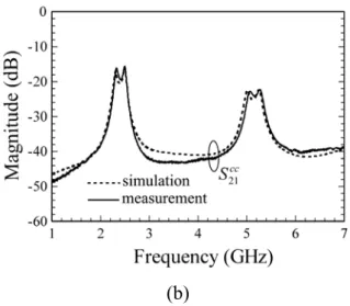
The proposed dual-band balanced BPF is simulated and verified by measurement of a fabricated circuit printed on an FR4 substrate. Results show that for the first (second) operating band of interest, the balanced BPF was measured to have a minimum differential- mode insertion loss of 3.03 dB (4.3 dB) and a minimum common-mode rejection level of as high as 15.7 dB (22.3 dB), as shown in Fig. 4.
(B) Balanced Dual-Band BPF with Stub- Loaded SIRs for CM Suppression [9]
In the second part of Section 4, a new fourth-order balanced dual-band BPF designed using four coupled bi-section half-wavelength (λ 2 ) SIRs is presented (see Fig. 5). To obtain the required DM operation with suppressed CM transmission, the SIRs were designed to have the same odd-mode, but different even-mode, resonant frequencies. For that purpose, the two inner SIRs were loaded at the center with T-shaped open stubs of different dimensions so that their even-mode resonant frequencies are shifted away from those of the outer SIRs and that their odd-mode ones remain almost intact.
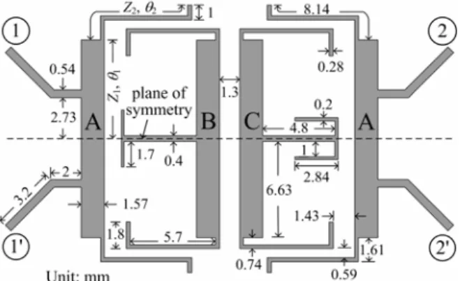
Fig. 5 Configuration of the proposed fourth- order balanced dual-band BPF using four coupled bi-section λ 2 SIRs.
The proposed balanced dual-band BPF is intended for use in the 2.4-GHz (2.4−2.484 GHz) and 5.2-GHz (5.15−5.35 GHz) WLAN bands and to be printed on a 0.635-mm-thick RT/Duroid 6010 substrate with a dielectric constant of 10.2 and a loss tangent of 0.0023. All the λ/2 SIRs should have the same odd-mode resonant frequencies of around 2.45 and 5.25 GHz, denoted by f1 and f3,
respectively. Assuming an equal electric length for the two sections of these SIRs (namely, θ θ1= 2 = ), the impedance ratio Rθ0 z
= Z2/ Z1 of the λ/2 SIRs can be found to be
2.42 using 1
(
)
3 1
tan Rz π 1 f f
− = + [13]. In
addition, the electric length of each line section is θ0=57.27° at 2.45 GHz.
Considering the precision limit of the fabrication process, the widths of Z1 and Z2
sections are set to 1.57 and 0.28 mm, respectively, which are equivalently 26.43 and 64 Ω in characteristic impedance.
With the dimensions of the basic SIRs available, we continue to determine the widths and lengths of the coupling gaps between the coupled λ/2 SIRs as well as the input/output tap positions. To proceed, we set the initial goal for the fractional bandwidths (FBWs) of the two passbands to be both 7%, which, to be on the safe side, is larger than the actually needed ones (namely, 3.4% and 3.8%, respectively, for the first and the second passbands of the proposed balanced BPF). Meanwhile, we use a fourth-order Butterworth
function as the target BPF response. The required external quality factor dd
e
Q of SIRs A at the two passband center frequencies can be calculated to be 10.93. The coupling coefficients between λ/2 SIRs can be found to be ABdd
M = MCAdd = 0.059 and MBCdd = 0.038, where dd
Mαβ, α β, =A, B,C stands for
the coupling coefficient between SIRs α and
β [14]. Once the external quality factor and the coupling coefficients are known, the gap width and the coupling length between the coupled λ/2 SIRs as well as the tap positions of the input/output SIRs can be determined by parametric studies through simulation [14].
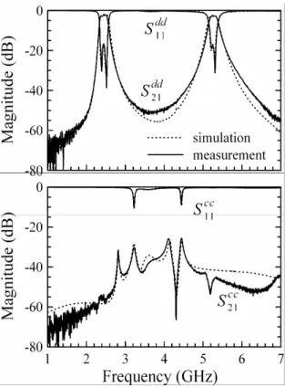
A prototype circuit of the proposed balanced dual-band BPF with structural parameters shown in Fig. 5 was fabricated and measured to verify its performance. Shown in Fig. 6 are the reasonably agreed simulated and measured S-parameters against frequency. For the DM response, the measured (simulated) first and second passbands are centered at 2.44 (2.45) and 5.25 (5.25) GHz, respectively, with 3-dB frequency ranges of 2.34−2.55 (2.34−2.58) and 5.14−5.38 (5.13−5.38) GHz. The measured (simulated) minimum insertion losses, respectively, are 2.4 (2) and 2.82 (2.33) dB for the first and second passbands. For the CM response, the measured (simulated) insertion loss is greater than 25 (25.6) dB in 1−7 GHz. Not shown in a figure for brevity, the measured amplitude imbalance ( S21 − S2 1′ ) (phase imbalance (∠S21− ∠S21' )) for the first
band is between 0.214 and 0.318 dB (178.31°and 181.61°) and that for the second band is between 0.285 and 0.433 dB (177.37°and 182.73°). The designed BPF circuit, with the feeding lines excluded, occupies an area of only 19.82 × 17.92 mm2.
Fig. 6 Simulated and measured S-parameters of the proposed balanced dual-band BPF for differential- and common-mode operations.
(C) Balanced Dual-Band BPF Using Only Equal-Electric-Length SIRS For Common- Mode Suppression [15]
In the third part of Section 2, a new fourth-order dual-band balanced BPF using only equal-electric-length (EEL) SIRS (see Fig. 7) and has very good CM suppression is presented. Again, the BPF is implemented on a low-loss RT/Duroid 6010 substrate. In this circuit design, the first and third resonant frequencies of the outer SIRs, also known to be their first two odd-mode resonant frequencies, are chosen the same as the two DM passband center frequencies of the BPF. The second resonant mode of the outer SIRs is indeed an even mode, whose existence always permits the CM transmission around the corresponding resonant frequency. To reduce the CM transmission, four additional EEL SIRs are inserted between the two outer SIRs and are designed to resonate only at the two odd-mode resonant frequencies of the outer EEL SIRs, not at the even-mode resonant frequency.
Fig. 7 Geometry of the proposed balanced dual-band BPF using only EEL SIRs.
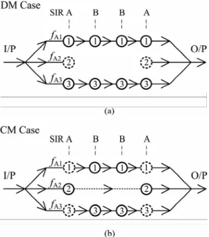
In Fig. 7, since SIRs A are deployed across the POS, their odd-mode resonance frequencies, fA1 and fA3, are the DM passband
center frequencies of the balanced BPF. On the other hand, since SIRs B are not deployed across the POS and are symmetrically located on both sides of the POS, all their resonant modes can be employed to support both the differential- and common-mode transmission. To block the common-mode transmission of the BPF, SIRs B must be designed not to resonate around fA2 (which is equal to
(fA1+fA3)/2, of course), the even-mode resonant
frequency of SIRs A. The reason for that can be more clearly elucidated using the signal-coupling schematics shown in Figs. 8(a) and 8(b) for DM and CM operations, respectively. In these schematics, a solid (dotted) circle with an enclosed number of i implies that the associated SIR can (cannot) resonate at fAi for the indicated operation mode
of the BPF (i.e., DM or CM). Moreover, a solid line section with an arrow signifies that the signal can be coupled or directly transmitted through it, whereas a dashed one suggests that the signal coupling is very weak because the two associated SIRs are too far apart.
As long as SIRs B are designed such that fB1 = fA1 and fB2 = fA3, DM transmission can be
established around fA1 and fA3, but not around fA2 (see Fig. 8(a)). For the CM operation
shown in Fig. 8(b), resonant signals excited in the input SIR A at fA2 are not likely to be
coupled to the adjacent SIR B because the latter does not resonate at that frequency.
Hence, these resonant signals in the input SIR A can only be very weakly coupled to the output SIR A that is far apart from the input one. In addition, although SIRs B can support the CM transmission of the BPF around fA1
and fA3, the signal transmission from the input
to the output around these two frequencies must be weak since SIRs A do not provide even-mode resonances around these two frequencies.
Fig. 8 Signal-coupling schematics for (a) DM and (b) CM operations
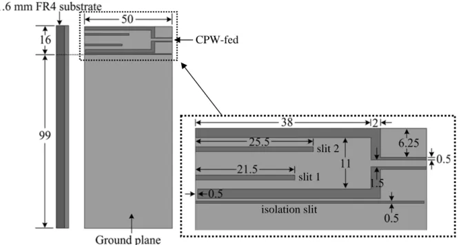
For validation, a balanced dual-band BPF that can be used in the 2.4-GHz (2.4−2.484 GHz) and 5.2-GHz (5.15−5.35 GHz) WLAN bands is designed on a 0.635-mm-thick RT/Duroid 6010 substrate. The detailed dimensions are shown in Fig. 7.
Fig. 9 shows the photograph of the fabricated BPF, which with the feeding lines excluded measures only 19.3 × 20.6 mm2. The
measured and simulated two-port DM and CM S-parameters shown in Fig. 10 are seen to agree well to each other. For the DM response, the measured (simulated) first and second passbands are centered at 2.476 (2.47) and 5.26 (5.25) and 5.26 (5.25) GHz, respectively, with 3-dB frequency ranges of 2.39−2.56 (2.38−2.56) and 5.14−5.38 (5.13−5.37) GHz. The measured (simulated)
minimum insertion losses, respectively, are 2.1 (2.2) and 2.55 (2.1) dB for the first and second passbands. For the CM response, the measured (simulated) insertion loss is greater than 33.3 (32.3) dB over the displayed frequency range of 1−7 GHz.
Fig. 9 The photograph of the fabricated balanced dual-band BPF.
(a)
(b)
Fig. 10 Simulated and measured S parameters of the proposed balanced dual-band BPF using only EEL SIRs. (a) DM and (b) CM operations.
4. Conclusions
All the main research topics included in the project proposal have been completed. Results were divided into several parts and
published in the well-known international journals such as “IEEE Microwave and Wireless Components Letters” and “Journal of Electromagnetic Waves and Applications” (Please see references [8], [9], and [15]). Results obtained from this research project are expected to serve as a useful reference for designers working in this field. The proposed dual-band abalanced BPFs will have practical value for use in the industrial area.
References
[1] G. Breed, Tutorial—Balanced circuits: A review of their operation and behavior, High Freq. Electronics, vol. 3, no. 8, pp.44−46, Sept. 2004.
[2] Wu, C. H., C. H. Wang, and C. H. Chen, “Novel balanced coupled-line bandpass filters with common-mode noise suppression,” IEEE Trans. Microwave Theory Tech. vol. 55, no. 2, pp. 287−295, Feb. 2007.
[3] Wu, C. H., C. H. Wang, and C. H. Chen, “Stopband-extended balanced bandpass filter using coupled stepped-impedance resonators,” IEEE Microw. Wireless Compon. Lett. vol. 17, no. 7, pp. 507-509, Jul. 2007.
[4] Wu, C. H., C. H. Wang, and C.H. Chen, “Balanced coupled-resonator bandpass filters using multisection resonators for common-mode suppression and stopband extension,” IEEE Trans. Microwave Theory Tech. vol. 55, no. 8, pp. 1756-1763, Aug. 2007.
[5] Lim, T. B. and L. Zhu, “Differential-mode wideband bandpass filter on microstrip mine for UWB application,” IEEE Microw. Wireless Compon. Lett. vol. 19, no. 10, pp. 632−634, Oct. 2009.
[6] Lim, T. B. and L. Zhu, “Differential-mode ultra-wideband bandpass filter on microstrip line,” Electronics Lett., vol. 45, no. 22, pp. 1124-1125, Oct. 2009.
[7] Chen, X., G. Han, R. Ma, J. Gao, and W. Zhang, “Design of balanced dual-band Bandpass Filter with self-feedback
structure,” ETRI Journal, vol. 31, no. 3., pp. 475-477, Aug. 2009.
[8] Lee, C.-H., I.-C. Wang, and C.-I. G. Hsu, “Balanced dual-band BPF using λ/4 stepped-impedance resonators and folded feed lines,” Journal of Electromagnetic Wave and Applications, vol. 23, no. 17/18, pp. 2441-2449, Dec. 2009.
[9] C.-H. Lee, C.-I G. Hsu, and C.-C. Hsu, “Balanced dual-band BPF with stub-loaded SIRs for common-mode suppression,” IEEE Microwave Wireless Compon Lett, vol. 20, no. 2, pp. 70-72, Feb. 2010.
[10] J. Shi and Q. Xue, “Balanced bandpass
filters using center-loaded half-wavelength resonators,” IEEE Trans
Microwave Theory Tech vol. 58, no. 4, pp. 970-977, Apr. 2010.
[11] J. Shi and Q. Xue, “Dual-band and wide-stopband single-band balanced bandpass filters with high selectivity and common-mode suppression,” IEEE Trans Microwave Theory Tech vol. 58, no. 8, pp. 2204−2212, Apr. 2010.
[12] J. Shi and Q. Xue, “Novel balanced dual-band bandpass filter using coupled stepped-impedance resonators,” IEEE Microwave Wireless Compon Lett, vol. 20, no. 1, pp. 19-21, Jan. 2010.
[13] M. Makimoto and S. Yamashita, “Bandpass filters using parallel coupled stripline stepped impedance resonators,” IEEE Trans. Microwave Theory Tech., vol. 28, no. 12, pp. 1413-1417, Dec. 1980.
[14] J.-S. Hong and M. J. Lancaster, Microstrip filters for RF/Microwave Application, John Wiley and Sons, pp. 129-159, 2001.
[15] Chung-I G. Hsu, Chih-Chan Hsu, Ching-Her Lee, and Shun-Hsiang Chen, ”Balanced dual-band BPF using only equal-electric-length SIRS for common-mode suppression,” Journal of Electromagnetic Waves and Applications, vol. 24, no. 5/6, pp. 695-705, 2010.
國科會補助專題研究計畫項下出席國際學術會議心得報告
日期:98 年 10 月 30 日計畫編號
NSC 98-2221-E-018-005
計畫名稱
應用於 WLAN 之雙頻平衡式帶通濾波器之設計
出國人員姓名
李清和
服務機構
及職稱
國立彰化師範大學 電子工程
學系暨電信工程研究所 教授
會議時間
98 年 10 月 20 日至
98 年 10 月 23 日
會議地點
泰國曼谷
會議名稱
2009 年國際天線與傳播論文研討會
The 2009 International Symposium on Antennas and Propagation
(ISAP 2009)
發表論文題目
應用於行動裝置之六頻帶天線設計
2009 年國際天線與傳播論文研討會(ISAP 2009)
(The 2009 International Symposium on Antennas and
Propagation (ISAP 2009))
(參加會議報告)
李 清 和 國立彰化師範大學 電子工程學系暨電信工程研究所 一、參加會議經過 國 際 天 線 與 傳 播 論 文 研 討 會 (International Symposium on Antennas and Propagation, ISAP )為亞洲及太平 洋地區知名之國際性天線與微波領 域會議,其內容包括天線(如各型多 頻、寬頻天線、小型天線、天線振陣 列等)與傳播、電磁量測、微波與射 頻技術、無線(衛星)通訊、導波理論 與結構、左手系材料與其應用及其他 相關領域等。ISAP 最早由日本發起, 過去每四年例行於日本舉行,近年則 每年舉辦一次。2009 年之 ISAP 則在 泰國曼谷舉行,會期由十月二十日至 同月二十三日,本次大會之總主席 (General Chair) 為 Dr. Prayoot Akkaraekthalin , 技 術 議 程 主 席 (Technical Program Chair) 為 Dr. Chuwong Phongcharoenpanich。 本年度會議共有來自全球 32 個 國家(主要為亞太地區),約 324 位學 者、專家及學生與會。365 篇論文被 接受做口頭發表或公開展示討論, 其中 7 篇為 invited papers。投稿論文 中有相當大之部份來自日本、台灣、 中國大陸、香港、韓國、新加坡、泰 國、印度、澳洲等。除了亞太地區外, 亦有少部份與會學者來自歐洲及美 洲。本年度國內相關領域之專家學者 及學生約有十餘人參加,在亞洲地區 國家中,除日本外,算是比較多的。 本年度會議於十月二十日報到 (註冊),當天下午進行五場之講習課 程,晚上並於會場所在皇后公園酒店 (Imperial Queen’s Park Hotel) Dinner Hall 舉行歡迎酒會。而技術性議程則 於十月二十ㄧ日至二十三日間分約 六十個場次依領域與順序進行口頭 論文發表。二十二日開幕式當天邀請 了國際天線學界之知名人士美國的 Dr. Prabhakar H. Pathak、日本的 Dr. Makoto Ando 及澳洲的 Dr Trevor S. Bird 分 別 主 講 三 場 之 keynotes speeches , 講 題 涵 蓋 大 型 天 線 之 分 析、應用於毫米波系統之平面波導陣 列及感測系統之天線等。 除了口頭論文發表外,主辦單位 為了能增進輪文研討效果,於十月二 十二日當天安排有優良論文之璧報 展示及論文競賽,讓與會者有面對面 討論之機會。此外,主辦單位亦邀了 數家贊助廠商於會場舉辦產品成果 或技術展示,以提供與學術界交流之 機會,例如 The Microwave Vision Group, BLUESET.se, FECO, CST Studio Suite, Agilent Technology 等。二、與會心得 在四天的研討會期中,大會在技 術議程期間每天依論文性質共安排 二十四個不同場次(上、下午各十二 場)同時進行論文發表和討論。綜觀 此次會議所提之論文主題,其領域涵 蓋了天線與傳播、小型(手機)天線、 多頻與寬頻天線、Patch 及陣列天 線 、 槽 線 (slot) 及 槽 孔 (aperturre) 天 線、適應型天線、MIMO 及 Diversity 天線、智慧型陣列天線、左手系物質 與其應用,以及天線相關之數值計算 方法等不少的研究方向,有些領域在 四天會期中有多個場次進行。其中與 筆者較相關之議題有小型天線與多 頻/寬頻天線等。 在多頻與寬頻天線方面,此次 ISAP 會議共有數個場次。論文之研 究重點主要集中在各種形狀與用途 之主動式與被動式(尤其是後者,包 括平面與非平面式)多頻與寬頻天線 結構設計、訊號饋入方式、增大頻寬 與縮小尺寸之技術及相關應用等,包 括模擬與實驗測試、驗證。 在及小型天線方面,設計之重點 主要在小型化及多頻或寬頻操作,以 方便能用於 thin-profile 之行動通訊 系統,例如手機、WLAN、及工作於 DCS 、 PCS 、 UMTS 、 WCDMA 、 Bluetooth 等多頻段之行動通訊裝置 等。 本年度之論文發表會,為了擴大 參與面,除了天線及相關主題外,亦 包括電磁數值計算及主動與被動微 波電路等之主題,各約有四個場次。 電磁數值計算方面,主要為各種數值 方 法 例 如 Method of moments 、 Constrained interpolation profile method、Equi-spaced-points method、 Time domain integral equation algorithmm、FDTD 等的新應用或新 型電磁系統模型之建立及更有效率 之數值方法之提出或已有方法之改 善等。被動微波電路方面則主要為新 的濾波器、baluns、波導裝置等之設 計、研發介紹。 本次會議在展示論文方面,為選 擇口頭報告論文中之較佳者參與,以 便有興趣者能有與作者進一步討論 之機會。論文展示會於週四上午舉 行,與會之學者相當多,且討論也相 當踴躍,文章則呈多面性。這些展示 論文作者亦成為本次大會論文競賽 之當然候選人,並由參觀者投票選出 優勝作品。值得一提者,本次前三名 之作品中,有一篇之作者即為來自台 灣。 三、建議 國內天線及微波方面之研究學 者近年來增加不少,尤其是天線方 面,主要集中在台大電機、電信、交 大電信、成大電機、中山電機、元智 通訊等校系所及中山科學院等,目前 都已有天線工程師學會之組織。此次 ISAP 會議即有近十餘篇之論文發 表,成果可說不錯。天線、微波與無 線通訊方面之研究,對國內發展電信 中心及通信產業界與國防科技等皆 相當重要。過去台灣在這方面之研究 位階不算頂尖,但這些年來由於政府 在相關科技研發及產業技術水平之 提升方面大力推動,且研究人才不斷 培育,已有長足的進展。
建議未來國科會、教育部及其他 政府部門可在此領域之支持可以再 予加強,尤其是經費方面。並多鼓勵 學者參與國際性論文研討會或由國 內 相 關 機 構 舉 辦 會 議 ( 今 年 ISAP 2009 期間,台灣之 IEEE AP-S Tainan Chapter 即申請、爭取 2012 年之 ISAP 在台灣舉行(但大會上未開會作最後 之決定)),以吸取各先進國家之經 驗,以期對國內相關學術研究及產業 之發展有更大之助益。 四、攜回資料 包括 ISAP 20096 會議議程及摘 要手冊與論文集光碟,參展廠商資 料,明年於日本橫濱舉行之 APMC 2010、於法國巴黎舉行之 European Microwave Week (含第 40 屆歐洲微 波會議、雷達會議及無線技術會議 等)、在加拿大多倫多舉行之 2010 APS、美國夏威夷舉行之 AP-S 2007 等論文研討會之徵稿資料等。 圖 1、ISAP 2009 大會開幕式。
Design of a Hexa-band Antenna for Mobile Devices
#
Po-Chun Cheng 1, Chow-Yen-Desmond Sim 3, Ching-Her Lee 1,2
1
Graduate Institute of Communications Engineering, National Changhua University of Education No. 2, Shi-da Rd., Changhua City, 500, Taiwan, R.O.C., [email protected]
2
Department of Electronic Engineering, National Changhua University of Education No. 2, Shi-da Rd., Changhua City, 500, Taiwan, R.O.C., [email protected]
3
Department of Electrical Engineering, Feng Chia University
No. 100, Wenhua Rd., Seatwen, Taichung 40724, Taiwan, R.O.C., [email protected]
1. Introduction
One of the most common antenna design for mobile devices is planar inverted-F antenna (PIFA) design [1-3], which normally covers the quad-band operation such as global system for mobile communication (GSM, 890-960 MHz), digital communication system (DCS, 1710-1880 MHz), personal communication system (PCS, 1850-1990 MHz), and universal mobile telecommunication system (UMTS, 1920-2170 MHz). Although this antenna design is attractive for achieving multi-band and broadband operations; however, it requires a top radiating patch that locates above the system ground plane, with a height commonly fixed at around 6 mm, thereby potentially increasing the thickness of the mobile devices. With the rapid growth in mobile communications, it is not until recently that dual-network system applications such as the wireless local-area network (WLAN) and worldwide interoperability for microwave access (WiMAX) are also being considered to incorporate into the mobile devices [4-5]. Hence, in this paper, a hexa-band internal printed co-planar antenna is proposed due to the advantages such as low-profile and easy to fabricate at low cost. Besides the ability to cover the usual GSM/DCS/PCS/UMTS band, the proposed antenna also includes the dual-network band operating at WLAN (2400-2480 MHz) and WiMAX (2500-2690 / 3400-3600 MHz). Details of the antenna design are described, and the measured results of all fabricated prototypes are presented and discussed.
2. Antenna Design
The geometry of the proposed internal printed co-planar monopole antenna fabricated on a single side of a FR4 substrate is depicted in Figure 1, showing a simple CPW-fed design occupying a small area of 50 × 16 mm2. Note that the lower left corner of the rectangular-shaped radiating element is linked back to the lower co-planar ground plane along the isolation slit, which in turn shorted to the circuit ground plane of 99 × 50 mm2. Two slits, slit 1 and slit 2, of length 21.5 and 25.5 mm, respectively, are embedded parallel to each other on the radiating element. Impedance matching can be achieved by tuning the gap distance between the radiating element and the CPW ground plane, which in this case is 2 mm.
3. Experimental Results and Discussion
The fabricated prototype antennas are initially studied by using the simulation software, and since the measured return loss results are well related to the simulated one, only the measured data is presented in Figure 2. In this figure, it demonstrates that the proposed antenna is stemmed from studying prototype A antenna (without embedding slits 1 and 2), which can excite a triple resonant modes at 960, 2250, and 3571 MHz. Besides these 3 resonant modes, if only slit 2 is embedded (prototype B), an additional mode at 1813 MHz will be stimulated due to the current distribution along this slit, and if only slit 1 is loaded (prototype C), an additional mode at around 1900 MHz will also be excited. Hence, by loading both the slits onto prototype A, the proposed antenna is formed and interestingly, improvement in impedance matching are observed for the lower (GSM) and upper (WiMAX, 3.5 GHz) band centred at 955 and 3353 MHz, respectively, with a measured
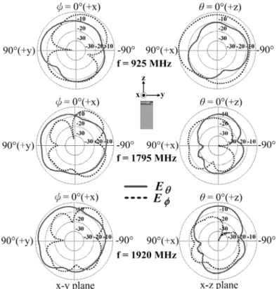
bandwidth of 210 and 753 MHz along 3:1 VSWR. As for the middle band for DCS/PCS/UMTS/WLAN/WiMAX (2.6 GHz) operation, a 1100 MHz bandwidth centred at around 2215 MHz is achieved due to combination of the 3 resonant modes, although the current distribution along slit 1 has caused a slight perturbation on the 2250 MHz mode. Figures 3 and 4 present the measured radiation characteristics of the proposed antenna at 2 principal planes at the centre frequencies of GSM, DCS, PCS, WLAN and WiMAX bands. Since the pattern for UMTS is similar to the DCS/PCS band, it is not presented here. The measured peak gain variation for all operating bands of the proposed antenna is presented in Figure 5, showing a stable gain variation of less than 2 dB. CPW-fed isolation slit slit 1 slit 2
Figure 1: Geometry of the proposed internal printed CPW-fed hexa-band antenna
VSWR 3:1
Figure 3: Measured radiation patterns for GSM, DCS, and PCS band
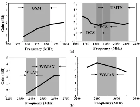
Figure 5: Measured peak gain variation of the proposed antenna for (a) GSM/DCS/PCS/UMTS, and (b) WLAN/WiMAX
References
[1] K. L. Wong, Y. C. Lin, “Thin internal planar antenna for GSM/DCS/PCS/UMTS operation in a PDA phone”, Microwave and Optical Technology Letters, vol. 47, No. 5, pp. 423-426, 2005. [2] H. Park, J. Choi, “Design of broad quad-band planar inverted-F antenna for
cellular/PCS/UMTS/DMB applications”, Microwave and Optical Technology Letters, vol. 47, No. 5, pp. 418-421, 2005.
[3] K. Seol, Y. Yang, J. Choi, “PIFA with PIL patch having bent feed line for GSM/DCS/UMTS/WiBro applications”, Electronics Letters, vol. 43, No. 8, pp. 436-437, 2007. [4] K. L. Wong, L. C. Chou, “Internal composite monopole antenna for WLAN/WiMAX operation
in a laptop computer”, Microwave and Optical Technology Letters, vol. 48, No. 5, pp. 868-871, 2006.
[5] C. I. Lin, K. L. Wong, S. H. Yeh, “Wideband EMC chip antenna for WLAN/WiMAX operation in the sliding mobile phone”, Microwave and Optical Technology Letters, vol. 48, No. 7, pp. 1362-1365, 2006.
國科會補助計畫衍生研發成果推廣資料表
日期 2010年11月01日國科會補助計畫
研發成果名稱
發明人
(創作人)
技術說明
技術移轉可行性及
預期效益
技術/產品應用範圍
產業別
計畫名稱: 計畫主持人: 計畫編號: 學門領域: (中文) (英文)成果歸屬機構
(中文) (英文) 應用於WLAN之雙頻平衡式帶通濾波器之設計 李清和 98 -2221-E -018 -005 - 電磁 具共模抑制之雙頻平衡式帶通濾波器A balanced dual-band bandpass filter with common-mode suppression
國立彰化師範大學 李清和,許智強,許崇宜 本作品為利用耦合式雙節步階式阻抗共振器(SIR)來設計可用於2.45 GHz及5.2 GHz WLAN通訊系統之雙頻平衡式帶通濾波器,兩個通帶可由式當設計SIR之長度 與調整其兩節維帶段之阻抗比來輕易達成。另外,藉由於內層兩個SIRs中央加 載T型開路殘段之方式,使該兩個SIRs之共模頻率與外側兩SIRs者錯開,如此讓 共模訊號無法於級間得到有效之耦合而被衰減,藉此可設計出差模特性極佳且 共模拒斥比高之施用雙頻平衡式帶通濾波器。
The proposed balanced dual-band bandpass filter (BPF) which is intended for application in WLAN systems is consructed using bi-secton stepped-impedance resonators. The two designated passbands can be easily designed by properly choosing the impedance ratio of the SIR. In addition, by loading at the centers of the two inner SIRs with T-shalpe open stubs to shift their even resonant-mode
frequencies, the common-mode (CM) signals can effectively be
attenuated. Thus a balanced BPF with good DM characteristics and high CM suppression can be obtained.
研究發展服務業 本作品具有產業利用價值,於WLAN通訊系統或相關產品均可應用到本技術。技術承接 單位人員則應具備通訊系統與微波電路之理論基礎及相關知識與背景,並具備電路製 作與測試、儀器量測與分析以及整合系統架構之能力。 本設計可技術移轉給相關產業之廠商,預估在無線網路卡等需要雙頻操作的系統應用 中,能降低電路成本、提高射頻電路操作特性,並達成產品縮小化之目標。
98 年度專題研究計畫研究成果彙整表
計畫主持人:李清和 計畫編號: 98-2221-E-018-005-計畫名稱:應用於 WLAN 之雙頻平衡式帶通濾波器之設計 成果項目 量化 單位 備 註 ( 質 化 說 明:如 數 個 計 畫 共 同 成 果、成 果 列 為 該 期 刊 之 封 面 故 事 ... 等) 實際已達成 數(被接受 或已發表) 預期總達成 數(含實際已 達成數) 本計畫實 際貢獻百 分比 國內 論文著作 期刊論文 0 0 100% 篇 研究報告/技術報告 1 1 100% 研討會論文 3 3 100% 專書 0 0 100% 專利 申請中件數 0 0 100% 件 已獲得件數 0 0 100% 技術移轉 件數 0 0 100% 件 權利金 0 0 100% 千元 參與計畫人力 (本國籍) 碩士生 5 5 100% 人次 博士生 0 0 100% 博士後研究員 0 0 100% 專任助理 0 0 100% 國外 論文著作 期刊論文 3 3 100% 篇 研究報告/技術報告 0 0 100% 研討會論文 1 1 100% 專書 0 0 100% 章/本 專利 申請中件數 0 0 100% 件 已獲得件數 0 0 100% 技術移轉 件數 0 0 100% 件 權利金 0 0 100% 千元 參與計畫人力 (外國籍) 碩士生 0 0 100% 人次 博士生 0 0 100% 博士後研究員 0 0 100% 專任助理 0 0 100%其他成果