二氧化鈦在高電子移動率電晶體上之應用
The Application of TiO
2on High-Electron-Mobility Transistor
研究學生:賴政弘 Student: Cheng-Hung Lai
指導教授:李冠慰 博士 Advisor: Dr. Kuan-Wei Lee
義守大學
電子工程學系
碩士論文
A Thesis Submitted toDepartment of Electronic Engineering I-Shou Universityin
Partial Fulfillment of the Requirements for the Master Degree with a Major in Electronic Engineering
July 2015 Kaohsiung, Taiwan
Republic of China
二氧化鈦在高電子移動率電晶體上之應用
賴政弘* 李冠慰** 義守大學電子工程學系 摘要 本論文為使用溶膠-凝膠法沉積二氧化鈦作為金氧半-變晶高電子移動率電晶體的 閘極氧化層,溶膠-凝膠混合溶液以旋轉塗佈均勻沉積於磷化銦表面。溶膠-凝膠法相較 於其他的氧化系統更為簡易且此方法不需要牽涉額外的能量,以高介電常數材料為元件 的閘極氧化物可減少表面狀態並且進一步改善元件的直流特性。 對於金氧半-變晶高電子移動率電晶體使用二氧化鈦為閘極氧化層而言,飽和電流 密度在閘極電壓相對源極電壓為 2 V 的偏壓下為 307 mA/mm,轉導的峰值為 193 mS/mm, 漏電流改善了 1 個數級,以金氧半-變晶高電子移動率電晶體而言,正向導通電壓為 7 V, 逆向崩潰電壓為-40 V。 關鍵字: 溶膠-凝膠法、二氧化鈦、閘極氧化層、磷化銦、變晶、金氧半、高電子移動 率電晶體 *:作者 :The Application of TiO2 on High-Electron-Mobility Transistor
Cheng-Hung Lai*, Kuan-Wei Lee**
Department of Electronic Engineering, I-Shou University
Abstract
The study uses solution gelation (sol-gel) processed titanium dioxide (TiO2) as gate oxide
layer of metal-oxide-semiconductor metamorphic high-electron-mobility transistor (MOS-MHEMT), the mixed solution was uniformly deposited on the surface of the InP Schottky layer using spin coating. The sol-gel method is simple compared with other oxide systems and this method need not involve excessive energy, the gate oxide using high permittivity may reduce the surface state and further improve the DC characteristics of device.
For MOS-MHEMT using TiO2 as gate oxide layer, the saturated drain current density is 307
mA/mm which bias at the gate to source voltage of 2 V, and the peak transconductance is 193 mS/mm, the gate current density improved one order of magnitude, for the MOS-MHEMT, the turn on voltage is 7 V, and the breakdown voltage is -40 V.
Keywords: solution gelation (sol-gel), titanium dioxide (TiO2), gate oxide, InP, metamorphic,
致謝
時光飛逝,幾年前還是大學新鮮人的我,轉眼間,從大學到研究所歷經了漫長的八 年終於要邁入尾聲而我的人生將要開啟新的一頁,首先,我要由衷感謝我的指導教授李 冠慰老師,從大四專題到研究所的求學途中,他不僅教導我很多的半導體製程方面的知 識,也教導我求學的態度,也時常教我許多待人處事的道理,更在我低迷時伸出援手將 我從谷底拉起,並且分享他的人生經歷以鼓勵我幫助我,使我感慨此生能與你這樣難得 的貴人相遇真的是我的福份,也希望未來還能有機會再與你合作。 感謝國立成功大學微電子所的王永和教授,提供寶貴的儀器和資源使我能夠在成大 的 AMD 實驗室做研究,在我儀器操作出問題時如嚴父般教導我其嚴重性並在我口試時給 予不少寶貴的建議,且於試後如慈父般的鼓勵我,令我難以忘懷。感謝黃榮生教授在我 半導體理論與模擬方面抽空指導我,使我了解許多半導體理論的一些數學推導與物理意 義並在我模擬有問題時提出很多的意見更想盡辦法幫助我化簡問題,在此感謝黃榮生老 師這段時間的幫忙與生活上的協助。 而在研究生的求學途中除了感激三位老師外,也特別感謝成大微電子的同學們智鈞 、元閔、承恩、祖儀、御琦、承融、建樺、育松在儀器的教導與熱心幫助。我也感謝跟 我同指導老師的義守同志泓偉、俊杰 、永捷在研究還有生活上的幫助跟鼓勵,讓我在 走到今日的路途中不至於孤寂,真的謝謝你們的幫助與陪伴。 在剛踏入碩士生活日期間我有幸能跟之前大學同學暐翔、峻豪、俊良、盛傑在同一 個屋簷下一起為碩士生活打拼,並且互相幫忙並分享自己的研究與實驗室的狀況。在碩 士階段進入後期,我有緣遇到宇謙、孟康這兩個可愛的學弟,感謝他們的幫助也因為他 們讓我在壓力中能獲得一些抒發,希望他們在未來裡能開創屬於他們自己的豐功偉業。 漫長的義大求學路程使我累積好多的回憶與點點滴滴,真的很感謝一路上的每一位 夥伴們,而我會好好珍惜這些回憶,最後要感謝我的父母與親戚,是他們在背後默默支 持鼓勵我讓我可以好好地走完大學到研究所這段路程。 政弘 2015 年 7 月List of Contents
Abstract (Chinese)
…...Ⅰ
Abstract (English)
...Ⅱ
致謝
...Ⅲ
List of Contents ...Ⅳ
List of Table ...Ⅵ
List of Figures ...Ⅶ
Chapter 1 Introduction ...1
1.1 Background and Motivation ...1
1.2 Organization ...3
Chapter2 Experimental Procedures and Characterization of Sol-Gel
Processed ... 5
Chapter 3 Fabrication Procedures of InAlAs/InGaAs MOS-
MHEMT ... 10
3.1 Device Structure ... 10
3.2 InAlAs/InGaAs MOS-MHEMT ... 11
Chapter4 The Performance of InGaAs/InAlAsMOS-MHEMT
... 23
4.1 Direct-Current Characteristics ... 23
4.1.1 The Drain Current Density... 23
4.1.2 The Transconductance ... 24
4.1.3 The Gate Leakage Current... 24
4.1.4 The Turn-on and Breakdown Voltage... 25
4.2 Numerical Simulation Results... 26
Chapter 5 Conclusion and Future Works ... 42
5.1 Conclusions ... 42
5.2 Future Works ... 42
List of Table
Table 1: The parameter of the simulated model………... 20 Table 2: DC characteristics of measurement for different devices in this
work ... 35
List of Figures
Chapter1
Fig.1-1 The organization chart of this study………..………... 4
Chapter 2 Fig. 2-1 The mixed solution preparation………...………... 6
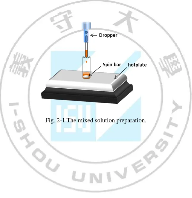
Fig. 2-2 Spin-coating a mixed solution on the sample……….. 7
Fig. 2-3 Soft baking ……….. 7
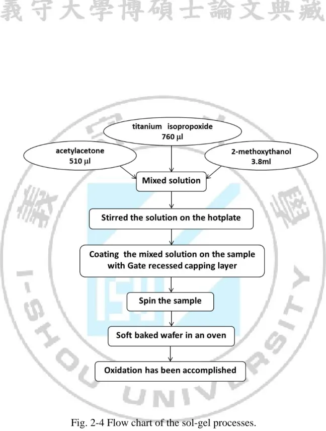
Fig. 2-4 Flow chart of the sol-gel processes ...……….. 8
Fig. 2-5 The oxidation of depositing the sol-gel processed TiO2 solution on InP schottky layer……….………… 9
Chapter 3 Fig. 3-1 Device substrate of this study ………...……... 14
Fig. 3-2 The cross-sectional view of (a) The conventional MHEMT and (b) The MOS-MHEMT with sol-gel TiO2……….……….. 15
Fig. 3-3 Step of the device fabrication (A) Mesa pattern defined, (B) Mesa isolation, (C) Removing the photoresist, (D) Source-drain pattern defined ...………. 16
Fig. 3-4 (E) Ohmic metal deposit, (F) Lift-off ohmic metal and photoresist, (G) Rapid thermal annealing, (H) Gate recess…….……….…… 17
Fig. 3-5 (I) Sol-Gel processed TiO2, (J) Gate pattern defined, (K) Gate metal deposit, (L) Lift-off gate metal and photoresist……… 18
Chapter 4
Fig. 4-1 The I-V characteristics of the conventional MHEMT………..27 Fig. 4-2 The I-V characteristics of the MOS-MHEMT……….. 28 Fig. 4-3 The drain current density and the transconductance versus gate voltage of the conventional MHEMT……….. 29 Fig. 4-4 The drain current density and transconductance versus gate voltages of the MOS-MHEMT………... 30 Fig. 4-5 The gate current density versus reverse gate voltages of the conventional MHEMT at VDS = 2 V, 2.25 V and 2.5 V….……… 31
Fig. 4-6 The gate current density versus reverse gate voltages of the MOS-MHEMT at VDS = 2 V, 2.2 V and 2.4 V……….. 32
Fig. 4-7 The turn-on voltage of MOS-MHEMT compared with conventional MHEMT………..………33 Fig. 4-8 The off-state breakdown voltage of MOS-MHEMT compared with conventional MHEMT……… 34 Fig. 4-9 The I-V characteristics which is amended by case 1... 36 Fig. 4-10 The I-V characteristics which is amended by case 2... 37 F i g . 4 - 1 1 T h e r e d u c e d I - V c h a r a c t e r i s t i c s a s s o c i a t e d w i t h F i g . 4-9 ……….……….…... 38 F i g . 4 - 1 2 T h e r e d u c e d I - V c h a r a c t e r i s t i c s a s s o c i a t e d w i t h F i g . 4-10 ...……….….………. 39 Fig. 4-13 The transconductance associated with Fig. 4-11…………...………. 40
Chapter 1
Introduction
1.1 Background and Motivation
The conventional Si-based semiconductor is already facing an issue of scaling limit of logical device, several researches about III-V compound semiconductors have developed in recent years, III-V compound semiconductors such as gallium arsenide (GaAs) and indium phosphide (InP) exhibited higher electron mobility and direct energy bandgap character compared well with Si.
The researches relating to the conventional high-electron-mobility transistors (HEMTs) stared in 1978 by Fujitzu [1], the operation of electron gas in HEMTs was somewhat different from field-effect transistors. The path of conduction electron is limited in two-dimensional gas (2DEG) further obtains the performance of high electron transport. Potential energy well was formed by heterojunction consists of a wide bandgap material and narrow bandgap material.
The heterojunctions containing InP substrate and InGaAs channel have achieved the high speed and high frequency application in the past few years [2]. Due to the InAlAs/InGaAs composite channel is not only lattice matched to InP, it also provide the high indium content for improving electron transport in the multiple quantum well.
high quality GaAs substrate are adaptable for large-scale millimeter wave integrated circuit application [3]. However, the InAlAs/InGaAs active layers with the increased in indium content, the lattice mismatch to GaAs substrate increase similarly. The lattice distortion thereby may obtain the lattice defects and dislocation on heterojunction and further decrease in performance of the device.
For solve above problem, the lattice matched buffer layers were grown on the GaAs substrate as metamorphic buffer, the material of the metamorphic buffer using similar indium mole compounds such as InAlAs. The graded InAlAs buffer layers grown on GaAs may effectively suppress the defect injected into the channel from substrate [4].
The GaAs based MHEMT with gate recessed schottky still suffered more problem such as higher gate leakage, lower breakdown voltage and narrow operation of gate voltage that may be attributed to the electrons trapped at the etched InP schottky surface.
In order to effectively overcome above problems, the gate oxide deposited on the schottky surface using high-k material has been researched in recent years. The high-k material such as SiO2 [5], Al2O3 [6], ZrO2 [7], HfO2 [8] and TiO2 [9],
the higher dielectric constant effectively enhance the performances of device contribute to high capacitance of this gate oxide.
TiO2 material had been widely application as the gate oxide due to its high
The TiO2 film growing on InGaAs [17, 18], AlGaAs [19], silicon [20] and
ITO [21] by sol-gel method have been reported. This thesis focus MOS-MHEMT with sol-gel processed TiO2 using easily operated spin coating.
The high coating uniform solvent rapidly obtained on InP surface by sol-gel method that further improve the DC characteristics of studied device comparing gate recessed HEMT [22].
1.2 Organization
This paper is divided into four chapters: Chapter 1: Introduction.
Chapter 2: Experimental Procedures and Characteristics of Sol-Gel Processed. Chapter 3: Fabrication Procedures of the InGaAs/InAlAs MOS-MHEMT. Chapter 4: The Performance of the InGaAs/InAlAs MOS-MHEMT. Chapter 5: Conclusion and Future Works.
The organization chart of this thesis is exhibited in Fig 1-1. Chapter 1 shows the background, motivation and organization of this thesis. Chapter 2 shows the preparation of sol-gel processed TiO2, we will describe the fabrication
procedures of the InGaAs/InAlAs MOS-MHEMT in chapter 3. In chapter 4, we will discuss the DC characteristics of MHEMT which compared with MOS-MHEMT, the finally conclusion and future work of this study will discuss in Chapter 5.
Chapter 2
Experimental Procedures and Characteristic of
Sol-Gel Processed
The experimental procedures of solution-gelation (sol-gel) processed titanium dioxide (TiO2) are prepared using the equipment consists of a dropper, a phial, a
magnetic stirrer, a stirrer bar, further depositing by spin casting and baking. The sol-gel systems in this study show in Figs. 2-1, 2-2 and 2-3. The flowchart about experimental procedures of sol-gel processed TiO2 is exhibited
in Fig. 2-4 and Fig. 2-5.
The advantages about sol-gel method are as followings [22, 23]: 1. Easy to control oxidation rate.
2. Low cost of this method compare with other oxidation process. 3. The oxidation system need not involve excessive energy.
4. Low controlled time for uniformity over on the sample rapidly. 5. Large-area oxide films obtained in this process.
The following steps of the sol-gel TiO2 procedures exhibited in below:
1. Sol-gel processed TiO2 prepared by mixed with oxide and Pentane-2, 4-dione
and 2-Methoxyethanol.
2. We placed dissolved solution in the shake table to stir the solution with a stirrer bar.
4. Spinning the sol-gel processedTiO2 using spin coater for obtaining uniformly
distributed thickness on the sample.
5. The final step about oxide bonding sample which is accomplished by baking the wafer in an oven.
Fig. 2-2 Spin-coating a mixed solution on the sample.
Fig. 2-5 The oxidation of deposited the sol-gel processed TiO2 solution on InP
Chapter 3
Fabrication Procedures of InAlAs/InGaAs
MOS-MHEMT
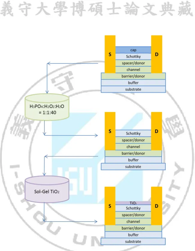
The gate recess using Phosphoric Acid mixture (H3PO4:H2O2:H2O) etch the
block of schottky layer, which obtain the roughness surface on the InP layer further causing the surface state. For solving above problem, we offer the oxidation about solution-gelation (sol-gel) process of the high-k TiO2 material.
The sol-gel processed TiO2 as gate oxide growing on InP surface that reduce the
gate leakage current.
In this study, The TiO2 solution mixed with Titanium isopropoxide (760 l)
and Pentane-2, 4-dione (510 l) and 2-Methoxyethanol (3.8 ml). After preparing above mixture, and placed this solution in the shake table to stir the solution. High-k oxidation process deposited by coating the sol-gel on the gate recessed schottky area of device and spin coated solution which attached to our samples, and then baking using oven for drying the moisture.
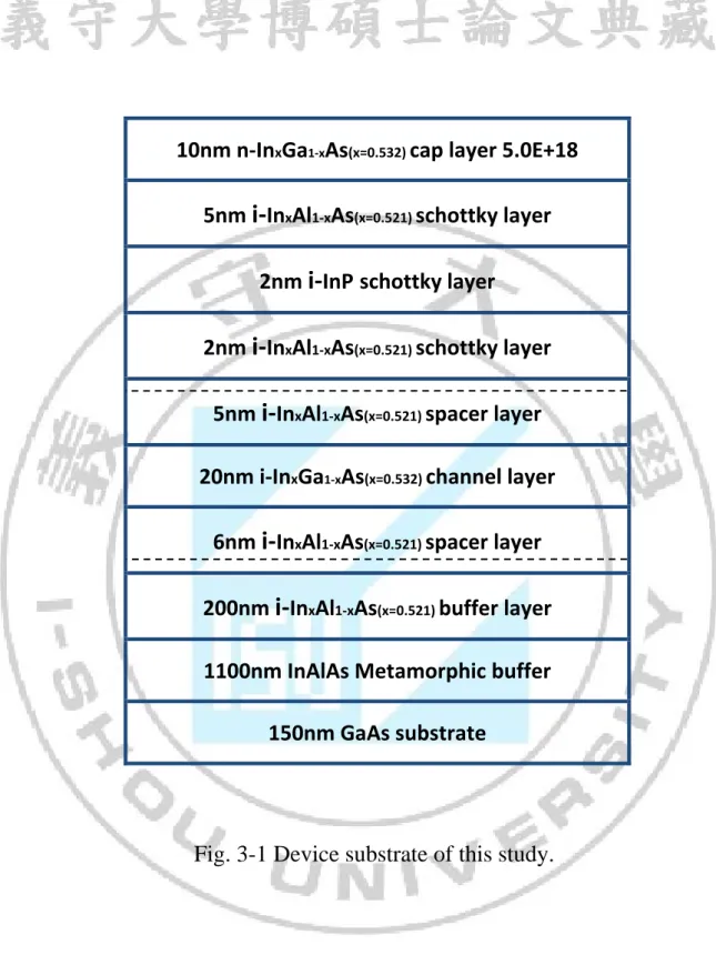
3.1 Device structure
layers, a undoped InP schottky layer, a 10nm InGaAs capping with a silicon doping density of 18
10
5 cm-3. The cross-sectional view of the device substrate
exhibited in Fig. 3-1.
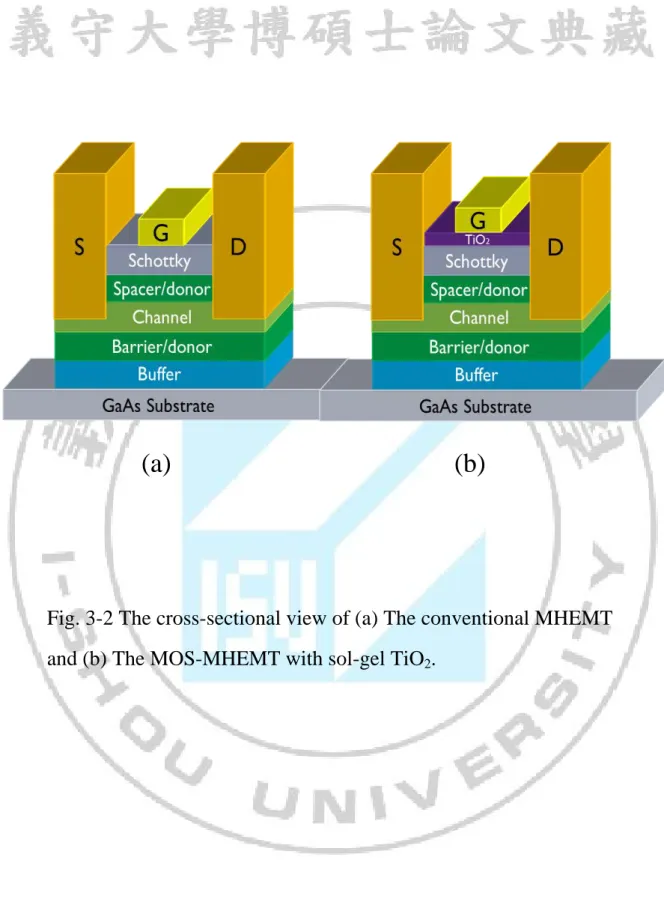
3.2InAlAs/InGaAs MOS-MHEMT
The experimental processes of sol-gel processed TiO2 as gate oxide for
InAlAs/InGaAs MOS-MHEMT with the gate dimensions are 100 1m2
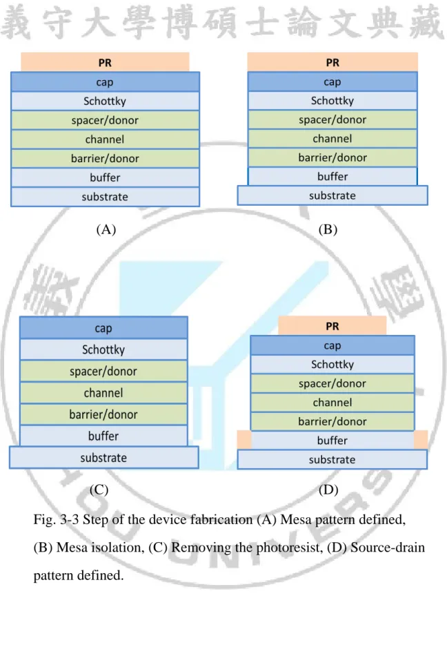
described in this section show in Figs. 3-2.The flow charts of MOS-MHEMT’s fabrication show in Figs. 3-3, 3-4 and 3-5. The related production methods of device as described below.
A. Mesa isolation
(1) In order to remove dust on the surface of the wafer, the wafers were cleaned by acetone, methanol, and DI water with ultrasonic vibration for 5 min.
(2) Coating the positive photoresist (I123) on the wafer and spin coated wafer by using spin coating at 7500 rpm for 37 s.
(3) Soft baked wafer on a hotplate at 90 ℃ for 5 min to dry the solvent in the photoresist.
(4) Mesa pattern defined by using DUV photolithograph aligner (Karlsuss MJB-3) to expose 8 s and then dip wafer in developer for 15 s to achieve development
(5) Mesa isolation defined was completed by wet etching Phosphoric Acid solution (H3PO4:H2O2:H2O = 1:1:20) to form an island region for prevent
(6) The wafer cleaned by immersing in the acetone for remove the photoresist.
B. Ohmic contact
(1) Coating the positive photoresist (I123) on the wafer and spin coated wafer by using spin coating at 7500 rpm for 37 s.
(2) Soft baked wafer on a hotplate at 90 ℃ for 5 min to dry the solvent in the photoresist.
(3) Ohmic pattern defined using a DUV photolithograph aligner (Karlsuss MJB-3) to expose 6 s and then dip the wafer in the developer for 15 s to achieve development.
(4) Ohmic metal deposition by evaporating AuGeNi alloy on the wafer.
(5) Lift off metal by immersing in heated PG remover and then clean the wafer in the IPA solution.
(6) Annealing the metal on Rapid thermal annealing (RTA) at 370 ℃ 50 s for forming the source-drain electrodes.
C. Gate recess and sol-gel process
(1) The sol-gel processed TiO2mixed with Titanium isopropoxide (760 l) and
Pentane-2, 4-dione (510 l) and 2-Methoxyethanol (3.8 ml) which placed in the shake table to stir the solution at last 18 hours.
(2) Gate recess accomplished by immersing the wafer in the Phosphoric Acid solution (H3PO4:H2O2:H2O = 1:1:40) to etch capping layer.
D. Gate pattern definition
(1) Coating the positive photoresist (I123) on the wafer and spin coated wafer by using spin coating at 7500 rpm for 37 s.
(2) Soft baked wafer on a hotplate at 90 ℃ for 5 min to dry the solvent in the photoresist.
(3) Gate pattern of the wafer defined by using DUV photolithograph aligner (Karlsuss MJB-3) to expose 8 s and then dip wafer in the developer for 30 s for 15 s to achieve development
(4) Gate metal deposition by evaporating gold (Au) on the oxide layer.
(5) Lift off metal by immersing in heated PG remover and then clean the wafer in the IPA solution.
(6) Fabrication of the device is completed and further measured the DC characteristics of the device.
Fig. 3-1 Device substrate of this study.
10nm n‐InxGa1‐xAs(x=0.532) cap layer 5.0E+18
5nm
i‐
InxAl1‐xAs(x=0.521) schottky layer 2nmi‐
InPschottky layer
2nm
i‐
InxAl1‐xAs(x=0.521) schottky layer 5nmi‐
InxAl1‐xAs(x=0.521) spacer layer 20nm i‐InxGa1‐xAs(x=0.532) channel layer 6nmi‐
InxAl1‐xAs(x=0.521) spacer layer 200nmi‐
InxAl1‐xAs(x=0.521) buffer layer 1100nm InAlAs Metamorphic buffer 150nm GaAs substrate(a)
(b)
Fig. 3-2 The cross-sectional view of (a) The conventional MHEMT and (b) The MOS-MHEMT with sol-gel TiO2.
Fig. 3-3 Step of the device fabrication (A) Mesa pattern defined, (B) Mesa isolation, (C) Removing the photoresist, (D) Source-drain pattern defined.
(A) (B)
Fig. 3-4 (E) Ohmic metal deposit, (F) Lift-off ohmic metal and photoresist, (G) Rapid thermal annealing, (H) Gate recess.
(E) (F)
Fig. 3-5 (I) Sol-gel processed TiO2, (J) Gate pattern defined,
(I) (J)
3.3Numerical Simulation Results
In this section, we focus on the simulation of gate recess MHEMT, this structure refer from, the y-axis is defined as the direction from the substrate to the gate and the x-axis is defined as the direction from the source to the drain. In this study, the numerical calculation domain is under the gate diode that indicated by red block, the base area of red block fallow the gate dimension
1 100 μm , the thickness from the gate to the channel expressed as (a1).
Permittivity in vacuum ∈ 8.854 10 F/cm Permittivity in InAlAs ∈ 12.73 ∈ F/cm Electron mobility μ 6500 cm / v ∙ s
Gate width W 100 μm
Gate length L 1 μm
The drain current of the HEMT at any y position is given by
I qn v w (3-1)
The electron drift velocity v is given by
v μ ε (3-2)
Inserting Eq. (3-2) into Eq. (3-1) we obtain
I qn μ ε W (3-3)
The electron field ε is related to potentialV as
ε (3-4)
The sheet carrier density is follow the Poisson equation [23] Table 1: The parameter of the simulated model.
The drain current is expressed as Eq. (3-6) using Eqs. (3-4) and (3-5)
I V V V μ W (3-6)
The integral of Eq. (3-6) from 0 to gate length (L) expressed by
I dx V V V μ WdV (3-7)
The integral of Eq. (3-7) is finally led to
I 2 V V V V (3-8)
When the transistor is operated at non saturation region:
0 V V
The equation of drain current density is expressed as
I = 2 V V V V ] (3-8)
When the transistor is operated at saturation region:
V V V , V V V V
The equation of drain current density is expressed as
I V V (3-9)
However, these equations of I-V curve haven’t to take non-ideal factors into consideration such as surface state and resistance effects. In addition, the thermal annealing of source/drain (S/D) metal of the simulated model which is desirable than somewhat of device fabrication, therefore the value of the drain current density will grow severely with increased gate to drain voltage and further cause breakdown of device.
In order to consider above non-ideal factors, the drain current density will be reduced by modifying some parameters of the simulated model that exhibited in below:
(1) The electron mobility has decreased from 9800cm / v ∙ s to 6500cm / v ∙ s according to surface state.
(2) The value of the saturation current density will be decreased threefold attribute to the effect on device resistance.
The results of modified drain current density can be divided into two cases and further discussing in chapter 4. The cases areas followings:
(1) The Vth is set to -0.2 V and the thickness (a1) may be gate recessed to 8nm.
Chapter 4
The Performance of InGaAs/InAlAs MOS- MHEMT
4.1 Direct-Current Characteristics
The DC measurement of studied device including current density-voltage curve (IDS), transconductance (gm), turn-on voltage (VON), breakdown voltage
(VBR) and gate current density (IGS) are discussed in this section.
4.1.1 Saturated Drain Current
The measured I-V curve of conventional MHEMT is exhibited in Fig. 4-1, the gate-to-source voltage (VGS) is biased from -2 V to 0.5 V in 0.5V step,
the saturated drain current density is 206.9 mA/mm at VGS = 0.5V. Fig. 4-2
shows the measured I-V curve of MOS-MHEMT, VGS is biased from -2 V to 2
V in 0.5 V step, the saturated drain current density is 307 mA/mm at VGS = 2 V.
Above MOS-MHEMT using sol-gel processed TiO2 as gate
dielectric increased the maximum operation of VGS due to high-k material
between oxide film and InP interface which provide a thick barrier to decrease the leakage current.
4.1.2 Transconductance
Transconductance (gm) of the definition following below equation:
The slope in this equation obtained by different in the value of drain current density (IDS) which associated which divided by associated VGS when the
drain-to-source voltage (VDS) is fixed in the saturation area [24].When the
drain-to-source voltage at 1 V, the maximumg of MHEMT is 230 mS/mm and the threshold voltage (Vth) is -1.25 V. The maximum g of the MOS-MHEMT
is 193mS/mm and Vth = -0.5 V.
4.1.3 The Gate Leakage Current
The measured gate current density versus the negative gate-to-source voltage of MHEMT and MOS-MHEMT with sol-gel processed TiO2 show in Fig. 4-5
and Fig. 4-6, respectively.
In this measurement, the bell-shaped behavior appear in the MHEMT but not in MOS-MHEMT, the high-k oxide decrease the impact ionization and further suppress hot electron causing in the narrow-bandgap channel.
4.1.4 The Turn-on and Breakdown Voltage
This section focused on the improved ability of DC characteristics. The measured turn-on and breakdown characteristics of conventional MHEMT and MOS-MHEMT with sol-gel processed TiO2 show in Fig. 4-7 and Fig. 4-8,
respectively.
The turn-on voltage (VON) obtained at the gate current as 1mA/mm, the
gate-to-source voltage sweeps from 0 V to the VON in 0.01 V step. The VTN
measured from conventional MHEMT and MOS-MHEMT are 0.5 V and 7 V, respectively.
The off-state breakdown voltage (VBR) of MHEMT and MOS-MHEMT
obtained at the gate current at -0.545 mA/mm and -0.398 mA/mm, respectively. The gate-to-source voltage sweeps from 0 V to the VBR in -0.01 V step. The VBR
measured from conventional MHEMT and MOS-MHEMT are -5 V and -40 V, respectively. The increasing VON and improved VBR in MOS-MHEMT with
4.2Numerical Simulation Result
The two cases of modified drain current density had exhibited in section 3.3. Fig. 4-9 shows the drain current density which has amended by case1andFig. 4-10 shows the drain current density which has amended by case 2, respectively.
However, the drain current density is still not conformed to the actual value of device fabrication. Therefore, we will adjust the current for attaining the actual value. Fig. 4-11 and Fig. 4-13 show the reduced I-V characteristics and associated gm which has adjusted from case 1, respectively. Fig. 4-12 and Fig. 4-14 show the reduced I-V characteristics and associated gm which has adjusted from case 2, respectively.
0.0 0.5 1.0 1.5 2.0 0 100 200 300 conventional MHEMT VGS = -2 V to 0.5 V, step = 0.5 V W / L = 100 m /1 m Dr a in c u rr e nt de n s it y (m A/ m m ) Drain-to-source voltage VDS (V)
0.0 0.5 1.0 1.5 2.0 2.5 0 100 200 300 400 MOS-MHEMT V GS = -2 V to 2 V, step = 0.5 V W / L = 100 m /1 m Dr ai n cur rent densi ty ( m A/mm) Drain-to-source voltage V DS (V)
-1.5 -1.0 -0.5 0.0 0.5 0 100 200 0 100 200 300 T ra n sco nduc tan c e (m S/ m m ) conventional MHEMT VDS = 1 V W / L = 100 m/1m Dra in cu rr ent d ensit y (m A/ m m ) Gate-to-source voltage VGS (V)
Fig. 4-3 The drain current density and the transconductance versus gate bias voltage of the conventional MHEMT.
-3 -2 -1 0 0 100 200 300 MOS-MHEMT VDS = 1 V W/L = 100 m /1 m D ra in c u rr e nt de n s it y ( m A /m m ) T ra ns c ondu c ta nc e ( m S /m m ) Gate-to-source voltage VGS (V) 0 100 200 300
Fig. 4-4 The drain current density and the transconductance versus gate bias voltage of the MOS-MHEMT.
V DS = 2 V V DS = 2.25 V V DS = 2.5 V -1.0 -0.8 -0.6 -0.4 -0.2 0.0 -0.55 -0.50 -0.45 -0.40 -0.35 -0.30 -0.25 -0.20 -0.15 -0.10 Gate-to-source voltage V GS (V) W/L = 100 m /1 m conventional MHEMT Gate c u rre nt d e ns ity (mA /mm)
Fig. 4-5 The gate current density versus reverse gate voltage of the conventional MHEMT at VDS= 2 V, 2.25 V and 2.5 V.
-2.4 -2.0 -1.6 -1.2 -0.8 -0.4 0.0 -0.050 -0.045 -0.040 -0.035 -0.030 -0.025 -0.020 -0.015 VDS = 2 V VDS = 2.2 V VDS = 2.4 V W/L = 100 m/1 m MOS-MHEMT G a te cur rent de nsit y ( m A/ mm) Gate-to-source voltage VGS (V)
Fig. 4-6 The gate current density versus reverse gate voltage of the MOS-MHEMT at VDS= 2 V, 2.2 V and 2.4 V.
0 1 2 3 4 5 6 7 8 0.0 0.2 0.4 0.6 0.8 1.0 MOS-MHEMT conventional MHEMT W/L = 100 m /1 m Gate c u rren t d ens ity (mA/mm) Gate-to-drain voltage VGD(V)
Fig. 4-7 The turn-on voltage of MOS-MHEMT compared with conventional MHEMT.
-45 -40 -35 -30 -25 -20 -15 -10 -5 0 5 1E-5 1E-4 1E-3 0.01 0.1 1 MOS-MHEMT conventional MHEMT W/L = 100 m /1 m Gate c u rren t de ns ity (mA/mm) Gate-to-drain voltage V GD (V)
Fig. 4-8 The off-state breakdown voltage of MOS-MHEMT compared with conventional MHEMT.
Table 2: DC characteristics of measurement for different devices in this work.
MHEMT MOS-MHEMT I mA/mm 206.9 307 gm (mS/mm) 230 193 Vt h (V) -0.5 -1.3 Vo n (V) 0.5 7 VB R (V) -5 -40
0.0 0.5 1.0 1.5 2.0 0 100 200 300 400 500 600 700 800 900 1000 conventional MHEMT V GS = -0.2 V to 0.7 V, step = 0.1 V W / L = 100 m /1 m Dr ai n c u rr ent dens ity ( m A/mm) Drain-to-sourcevoltage V DS (V)
0.0 0.5 1.0 1.5 2.0 0 100 200 300 400 500 600 700 800 900 1000 conventional MHEMT V GS = -0.5 V to 0.5 V, step = 0.1 V W / L = 100 m /1 m Drain curr ent density ( m A/mm ) Drain-to-source voltage VDS (V)
0.0 0.5 1.0 1.5 2.0 0 100 200 300 conventional MHEMT V GS = -0.2 V to 0.7 V, step = 0.1 V W / L = 100 m /1 m Dr ai n c u rr ent densi ty ( m A/mm) Drain-to-source voltage V DS (V)
0.0 0.5 1.0 1.5 2.0 0 100 200 300 400 conventional MHEMT V GS = -0.5 V to 0.5 V, step = 0.1 V W / L = 100 m /1 m Dr ai n c ur rent dens it y ( m A/mm) Drain-to-source voltage VDS (V)
-0.70 -0.35 0.00 0.35 0.70 0 100 200 300 Gate-to-source voltage VGS (V) conventional MHEMT V DS = 1 V W / L = 100 m /1 m D ra in c u rr e nt de ns it y ( m A /m m ) T ra n s c o n duc ta nce ( m S /m m ) 0 100 200 300 400 500 600
-1.0 -0.5 0.0 0.5 0 100 200 300 0 100 200 300 400 500 600 T ra n s c on duc ta nc e ( m S /m m ) conventional MHEMT VDS = 1 V W / L = 100m /1m Dr ai n c u rr en t d en s it y (m A /m m ) Gate-to-source voltage VGS (V)
Chapter 5
Conclusion and future works
5.1 Conclusions
The InGaAs/InAlAs MOS-MHEMT using sol-gel processed TiO2 as gate
dielectric in this thesis exhibited excellent DC characteristics compared with gate recessed HEMT, such as higher maximum drain current density widely rang of voltage operation, larger breakdown character, better turn-on voltage and reduced gate leakage current density.
MOS-MHEMT with high-k gate insulator contributed to enhance the maximum current density and also obtain a decreased surface state to suppress the impact ionization effect from the InGaAs channel layer. Therefore, the high permittivity gate insulator deposited on InP surface using sol-gel process that is suitable for power application.
5.2 Future Works
The sol-gel process after passivation treatment on schottky surface of MOS-MHEMT somewhat could be considered a promising procedure for
Reference
[1] T. Mimura, S. Hiyamizu, T. Fujii, and K. Nanbu, “A new field-effect transistor with selectively doped GaAs/n-AlxGa1-xAs heterojunctions,” Jpn.
J. Appl. Phys, vol. 19, pp. 225, 1980.
[2] Y. C. Chen, D. L. Ingram, R. Lai, M. Barsky, R. Grunbacher, T. Block, H. C. Yen, and D. C. Streit, “A 95-GHz InP HEMT MMIC amplifier with 427-mW power output,” IEEE Microwave and Guided Wave letters, vol. 8, no. 11, 1998.
[3] C. C Huang, Y.J. Liu, T. Y. Chen, C. S. Hsu, C. I. Kao, and W. C. Liu, “Improved thermal stability performance of an MHEMT with a double δ-doped structure,” Electrochemical and Solid-State Letters, vol. 14, issue. 1, 2011.
[4] C.S. Lee, C. J. Chian, W. C. Hsu, K. H. Su, and S. J. Yu, “channel-composition-dependent characteristics of δ -doped InxAl1-xAs/InyGa1-yAs metamorphic high electron mobility transistors,”
Journal of the Korean Physical Society, vol. 52, no. 4,pp. 1086-1092, 2008.
[5] L. Pang, Y. Lian, D. S. Kim, J. H. Lee, and K. Kim, “AlGaN/GaN MOSHEMT with high-quality Gate–SiO2 achieved by room-temperature
radio frequency magnetron sputtering,” IEEE Transactions On Electron
Devices, vol. 59, no. 10, pp. 2650-2655, 2012.
[6] P. D. Ye, B. Yang, K. K. Ng, J. Bude, G. D. Wilk, S. Halder, and J. C. M. Hwang, “GaN MOS-HEMT using atomic layer deposition Al2O3 as gate
dielectric and surface passivation,” International Journal of High Speed
[7] S. Abermann, G. Pozzovivo, J. Kuzmik, G. Strasser, D. Pogany, J. F. Carlin, N. Grandjean, and E. Bertagnolli, “MOCVD of HfO2 and ZrO2 high-k gate
dielectrics for InAlN/AlN/GaN MOS-HEMTs,” Semicond. Sci. Technol, vol.22, no.12, pp. 1-4, 2007.
[8] X. Sun, O. I. Saadat, K. S. Chang-Liao, T. Palacios, S. Cui, and T. P. Ma, “Study of gate oxide traps in HfO2/AlGaN/GaN MOS-HEMTs by use of ac
transconductance method,” Applied Physics Letters, vol. 102, no. 103504, 2013.
[9] B.Y. Chou, C. S. Lee, C. L. Yang, W. C. Hsu, H. Y. Liu,M. H. Chiang, W. C. Sun, S. Y. Wei, and S. M. Yu, “TiO2-dielectric AlGaN/GaN/Si
MOS-HEMTs by using nonvacuum ultrasonic spray pyrolysis deposition,”
IEEE Electron Device Letters, vol. 35, no. 11,2014.
[10] T. S. Yang, C. B. Shiu, and M. S. Wong, “Structure and hydrophilicity of titanium oxide films prepared by electron beam evaporation,” Surface
Science,vol. 548, issues 1-3, pp. 75-82, 2004.
[11] M. K. Lee, and C. F. Yen, “InP schottky barrier MOSFET withTiO2/Al2O3
as gate oxide,” Computer, Consumer and Control (IS3C), 2014
International Symposium on, Taichung, Taiwan, June. 10-12, 2014, pp.
573–576.
[12] G.A. Battiston, R. Gerbasi, A. Gregori, M. Porchiaa, S. Cattarin, and G.A. Rizzi, “PECVD of amorphous TiO2 thin films: effect of growth
[14] T. Y. Wu, S. K. Lin, P. W. Sze, J. J. Huang, W. C. Chien, C. C. Hu, M. J. Tsai, and Y. H. Wang, “AlGaN/GaN MOSHEMTs with liquid-phase-deposited TiO2 as gate dielectric,” IEEE Transactions on
Electron Devices, vol. 56, no. 12, 2009.
[15] P. Kajitvichyanukul, J. Ananpattarachai, and S. Pongpom, “Sol–gel preparation and properties study of TiO2 thin film for photocatalytic
reduction of chromium (VI) in photocatalysis process,” Science and
Technology of Advanced Materials, vol. 6, no.3-4, pp. 352–358, 2005.
[16] D. Rathee, M. Kumar, and S. K. Arya, “Deposition of nanocrystalline thin TiO2 films for MOS capacitors using Sol–Gel spin method with Pt and Al
top electrodes,” Solid-State Electronics, vol.76, pp. 71–76, 2012.
[17] C. C. Hu, C. E. Wu, H. C. Lin , K. W. Lee, and Y. H. Wang “Enhancement-mode In0.53Ga0.47As MOSFETs with sol–gel processed gate
dielectrics,” Materials Science in Semiconductor Processing, pp. 272–276, vol. 29, 2015.
[18] C. E. Wu and Y. H. Wang, “Enhancement mode In0.53Ga0.47As metal oxide
semiconductor field effect transistors with solution processed gate insulator,” National Cheng Kung University, July 2012.
[19] K. Ozasa, S. Nemoto, M. Hara a, M. Maeda, and K. Mochitate, “The passivation/modification of AlGaAs/GaAs surfaces by amorphous TiO2 for
the bio-sensing use in electrolytes,” Surface Science 601, pp. 4536–4540, 2007.
[20] D. Rathee, S. K. Arya, and M. Kumar, “Capacitance–voltage analysis of a high-k dielectric on silicon,” Journal of Semiconductors, vol. 33, no. 2, 2012.
[21] P, C, Yao, M. C. Lee, J. L. Chiang, “Annealing effect of Sol-gel TiO2 thin
film on pH-EGFET sensor,” Computer, Consumer and Control (IS3C),
2014 International Symposium on,Taichung, Taiwan, June. 10-12, 2014, pp.
577 – 580.
[22] J. S. Huang, C. H. Lai, H. W. Chen, Y. C. Chang, Y. H. Wang, and K. W. Lee, “Sol-gel processed TiO2 on InP and its application,” IEEE
International Symposium on Next-Generation Electronics 2015 (ISNE 2015),Taipei, Taiwan, May. 4, 2015, pp. 577 – 580.
[23] K. Kajihara, “Recent advances in sol–gel synthesis of monolithic silica and silica-based glasses,” Journal of Asian Ceramic Societies, vol. 1, no. 2, pp. 121–133, 2013.
[24] F. Schwierz and JJ. Liou, “Modern microwave transistors: theory, desigh, and performance,” USA, New Jersey, John Wiley & Sons, Inc, 2002.