ers grown by the atomic layer chemical vapor deposition are char-acterized as a function of the Hf concentration and the annealing temperature. The peaks of Fourier transform infrared spectra at 960, 900, and 820 cm−1originate from Hf–O–Si chemical bonds, revealing that a Hf-silicate interfacial layer began to form at the HfO2/SiO2 interface after postdeposition annealing process at
600◦C for 1 min. Moreover, the intensity of the peak at 750 cm−1 can indicate the degree of crystallization of HfO2. The formed
Hf-silicate layer between HfO2 and SiO2 is also confirmed by
X-ray photoelectron spectroscopy.
Index Terms—Fourier transform infrared (FTIR), HfO2,
Hf-silicate, high-k, X-ray photoelectron spectroscopy (XPS), X-ray reflectivity (XRR).
I. INTRODUCTION
I
N ORDER TO meet the International Technology Roadmap for Semiconductor [1] requirements for equivalent oxide thickness (EOT) and gate leakage current, the conventional SiO2 gate dielectric might need to be replaced by higher dielectric constant materials [2]. Using the “high-k dielectric” allows the device to maintain an EOT of 1 nm or less, while having a larger physical thickness to reduce the tunneling cur-rent. Among the various high-k dielectric materials, hafnium-based dielectrics are being widely investigated due to their high dielectric permittivity, high melting point, and accept-able thermal and chemical stabilities [3]–[6]. However, the hafnium-based dielectrics still have some critical issues, suchManuscript received May 8, 2006; revised December 19, 2006. The work of the National Taiwan University group was supported by the National Science Council, Taiwan, R.O.C., under Contract 93-2215-E-002-003 and Contract 93-2215-E-002-017. The review of this paper was arranged by Editor G. Groeseneken.
T. C. Chen, C.-Y. Peng, and C.-H. Tseng are with the Department of Elec-trical Engineering and Graduate Institute of Electronics Engineering, National Taiwan University, Taipei 10617, Taiwan, R.O.C.
M.-H. Liao, M.-H. Chen, and C.-I Wu are with the Department of Electrical Engineering and Graduate Institute of Electro-Optical Engineering, National Taiwan University, Taipei 10617, Taiwan, R.O.C.
M.-Y. Chern is with the Department of Physics, National Taiwan University, Taipei 10617, Taiwan, R.O.C.
P.-J. Tzeng is with the Electronics Research and Service Organization, Industrial Technology Research Institute, Hsinchu 310, Taiwan, R.O.C.
C. W. Liu is with the Department of Electrical Engineering, Graduate Institute of Electronics Engineering, and Graduate Institute of Electro-Optical Engineering, National Taiwan University, Taipei 10617, Taiwan, R.O.C. (e-mail: [email protected]).
Digital Object Identifier 10.1109/TED.2007.892012
[8], which impede their industrial application. Furthermore, it is hard to maintain the amorphous state for HfO2 due to its low crystallization temperature (300 ◦C−400◦C) [9]. The pseudobinary materials, such as Hf-aluminate and Hf-silicate, combine the advantages of acceptable dielectric constant and desirable higher crystallization temperature [10]. Therefore, the material change of high-k dielectrics after the thermal process is a significant issue for the future CMOS applications. In this paper, we investigate the material and electrical modification of Hf-based dielectrics at different annealing conditions and different Si incorporations.
II. EXPERIMENT
The high-k films were on the 15–25 Ω· cm p-type Si wafers. All samples were treated with an SC-1 preclean process before high-k dielectrics deposition. This cleaning process typically results in a chemical oxide layer between high-k dielectrics and the Si substrate to enhance initial growth of the high-k dielectrics. The HfO2 and Hf-silicate films were deposited by hot-wall atomic layer chemical vapor deposition [11] with a reaction temperature of 300 ◦C, using alternating surface-saturation reactions of HfCl4, SiCl4, and H2O. Note that Hf-silicate films with different Hf/Si ratios (Hf0.38Si0.62O2, Hf0.5Si0.5O2, and Hf0.66Si0.34O2) were grown using alternated nanomixed HfO2/SiO2[12]. After deposition, a silicon nitride cap to form a thin passivation layer (< 0.5 nm) was deposited at 600 ◦C for 10 s using NH3 and SiCl4 precursors. The samples were annealed in the furnace at 600◦C for 1 min and 1000◦C for 5 min in N2ambient for postdeposition annealing (PDA). The furnace was kept at the atmospheric pressure and purged by nitrogen. The electrical properties were studied using metal–insulator–semiconductor (MIS) capacitors with a 50-nm-thick Pt electrode deposited by E-gun and a circular area of 2.5× 10⁻⁴ cm2 defined by the shadow mask. Another Al contact is deposited on the back of the sample. The postmetal-lization annealing (PMA) was done in forming gas, N2(90%) + H2(10%), at 400◦C for 30 min before the electrical measure-ment. Fourier transform infrared (FTIR) spectroscopy was used to observe transmission spectra of the different chemical bonds and the change of bonding state after thermal processing. Each spectrum was measured with a resolution of 4 cm−1 and a range of 370–1800 cm−1 and transformed from transmission
760 IEEE TRANSACTIONS ON ELECTRON DEVICES, VOL. 54, NO. 4, APRIL 2007
Fig. 1. (a) Scheme of FTIR measurement structure. (b) FTIR spectra of HfO2
after PDA at 600◦C for 1 min in flowing N2 measured by “face-to-face”
structure. The intensity of IR signal with ultrathin high-k layer can be enhanced by the “face-to-face” method.
Fig. 2. FTIR spectra of ultrathin HfO2films as-deposited, annealed at 600◦C
for 1 min, and annealed at 1000◦C for 5 min in N2ambient. The positions of
the peaks in the three curves are indicated by dashed lines. The intensity of the peak at 750 cm−1is clearly seen to increase the thermal budget.
to absorption. High-resolution transmission electron micro-scope (HRTEM) and X-ray photoelectron spectroscopy (XPS) were used for physical thickness inspection and observation of the chemical composition of the gate dielectrics. X-ray reflectivity (XRR) using CuKα source was used to study the constituent thickness and roughness of these films. The thick-ness obtained by XRR was calibrated with HRTEM
measure-Fig. 3. FTIR absorption spectra of Hf-silicate. The samples in (a) were not annealed, and in (b) and (c), the samples were annealed in N2 ambient for
1 min at 600◦C and for 5 min at 1000◦C, respectively. There are only two peaks (at 600 and 512 cm−1) in the as-deposited nanomixed HfO2/SiO2,
indicating no Hf-silicate formation.
ments for layer thickness and atomic force microscopy (AFM) for surface roughness. The electrical properties of HfO2 and Hf-silicate films on chemical oxide with different PDA condi-tions were also studied. The capacitance–voltage (C–V ) and current–voltage (I–V ) characteristics for electrical properties were measured with HP 4284A and Keithley 4200 instruments, respectively.
Fig. 4. XPS results of the (a) Hf 4f, (b) O 1s, and (c) Si 2p peaks for HfO2films as-grown and annealed at 1000◦C for 5 min in N2ambient. The shift of the
Hf 4f, O 1s, and Si 2p peaks to higher binding energy is due to the formation of a Hf-silicate layer.
III. RESULTS ANDDISCUSSION
A. FTIR Results
FTIR analysis is a reliable and powerful method due to its convenient, rapid, and nondestructive measurement. However, the high-k gate dielectrics are too thin to detect in FTIR measurement, and the characteristics of a thin HfO2 layer may be quite different from those of a thick one due to the crystallization [13]. Previous work has shown that it is possible to detect the chemical bonding vibrations of SiO2, HfO2, and hydrogen defects in layers as thin as several nanometers using attenuated total reflection and multiple internal reflection measurements [14]–[16]. Those techniques use a complicated method to adjust the incident angle of the IR beam to enhance the signal. A simple method to detect the weak signal from the ultrathin film and from the interface between the high-k layer and the oxide is reported here. A schematic cross section of our “face-to-face” measurement structure is shown in Fig. 1(a). The absorption is enhanced in the “face-to-face” structure due to the doubling of the film thickness and the reflection at the interface between the surfaces of two samples. Note that there is no observable absorption signal if we use only one sample in our measurement system. Fig. 1(b) shows the FTIR spectra of HfO2 after annealing at 600 ◦C for 1 min by the “face-to-face” measurement structure. Fig. 2 shows the FTIR spectra of the as-deposited HfO2sample and the HfO2samples annealed at 600◦C (1000◦C) in N2ambient for 1 min (5 min). There are three peaks, at 750, 600, and 512 cm−1, attributed to the Hf–O chemical bonds in the spectra, and the peaks at 960, 900, and 820 cm−1 are assigned to Hf–O–Si stretching vibrations [17]–[19]. The peak at around 1120 cm−1may result
from the absorption by the Si–N bond [20] formed by surface nitridation or from Si–O–Si bond absorption in the chemical oxide layer. The as-deposited HfO2 film spectrum exhibits peaks at 600 and 512 cm−1 due to Hf–O chemical bonds, and these two peaks increase with annealing temperature, so does the 750 cm−1peak. The intensity of the 750 cm−1 peak increases with the thermal budget of the HfO2 due to the increasing degree of crystallization [21]. Comparing the three spectra (as-deposited, annealed at 600 ◦C, and annealed at 1000◦C), the intensities of the peaks at 960, 900, and 820 cm−1 are seen to increase with the thermal budget. This is due to the Hf–O–Si chemical bonds formed at the HfO2/SiO2interface. The formation of silicate cannot be avoided during the thermal process. During the annealing process, Hf-silicate is formed by the atomic diffusion mechanism [22]. As a result of Si diffusion into HfO2, the Hf-silicate should be formed in the original HfO2layer, thus increasing the interfacial layer thickness. The silicate interfacial layer shows no obvious contrast with the initial chemical oxide in the transmission electron microscopy (TEM) image (Fig. 5), indicating that the interfacial silicate might be Si rich. In Fig. 3, the FTIR absorption spectra of Hf-silicate are shown as a function of Hf concentration at differ-ent thermal annealing conditions. In Fig. 3(a), the as-deposited samples show no apparent peaks from 700 to 1000 cm−1, which indicates that the as-deposited nanomixed HfO2/SiO2 does not intermix, whereas the peaks at 600 and 512 cm−1 are detected in as-deposited nanomixed HfO2/SiO2, indicating Hf–O bond formation. The annealing at 600 ◦C and 1000◦C generates absorption peaks due to Hf–O–Si stretching vibra-tions [Fig. 3(b) and (c)], indicating the intermixture and forma-tion of Hf-silicate after the thermal annealing of the nanomixed
762 IEEE TRANSACTIONS ON ELECTRON DEVICES, VOL. 54, NO. 4, APRIL 2007
Fig. 5. HRTEM cross-sectional images of HfO2 (a) as-deposited, (b) after
600◦C/1 min/N2 annealing, and (c) after 1000 ◦C/5 min/N2 annealing.
The thickness of the interfacial layer between HfO2 and Si is increased by
annealing.
HfO2/SiO2. Moreover, the intensity of the peak at 750 cm−1 also increases the Hf concentration in Fig. 3(b) and (c), indi-cating slight occurrence of phase separation and crystallization at the high Hf concentration [23]. Due to the variation in each measurement, in Fig. 3, the intensity of oxide has been normalized. The integration of the Hf–O–Si peak area is only studied as a function of temperature in the Hf0.66Si0.34O2 samples. The ratio of this sample with PDA at 600◦C for 1 min and PDA at 1000◦C for 5 min is 2, which indicates the increase of Hf–O–Si bonds with the increase of temperature. Note that,
Fig. 6. XRR spectra of HfO2film as-deposited, after 1-min annealing in N2
at 600◦C, and after 5-min annealing in N2at 1000◦C. The inset is the surface
roughness for HfO2samples by AFM. The roughness of the HfO2surface is
lower than 0.5 nm even after high-temperature annealing.
although the HfO2 sample seems to have more pronounced Hf–O–Si peak (Fig. 2) than the nanomixed HfO2/SiO2samples [Fig. 3(c)], the integration of the Hf–O–Si peak area (filtering the background of the broad signal) is slightly lower than the nanomixed HfO2/SiO2 samples. The quantitative analysis of the FTIR signal is not obtained by the difference of the optical alignment and environmental condition for each measurement.
B. Structural Analysis
The HfO2 film on SiO2 following PDA at 1000◦C is also characterized by XPS measurements, as shown in Fig. 4. In Fig. 4(a), the peak of the XPS of HfO2after the PDA process is at about 17.9 eV. The shift of Hf peak to higher binding energy is attributed to the formation of Hf-silicate film, which is 0.5 eV higher than that of the as-grown HfO2film (17.4 eV). Note that the two peaks (Hf 4f7/2 and Hf 4f5/2) of XPS in Hf element cannot be distinguished due to the limit of resolution of the XPS equipment. Furthermore, the O 1s spectrum [Fig. 4(b)] and Si 2p spectrum [Fig. 4(c)] of the annealed samples are also shifted to higher energy as compared to those of as-grown sample, indicating a strong signature of Hf-silicate formation. The intensity of reflected X-ray is dependent on the surface and near-surface electron density. Consequently, XRR has been used to study a variety of surface and thin film properties. In order to understand the effects of the PDA process, it is important to realize the effect on the chemical reaction at interface and the growth of the interfacial layer due to the increasing thermal budget. XRR and TEM have been utilized to analyze the physical characteristics of as-grown and postan-nealed HfO2. The TEM images of HfO2thin films as-deposited, annealed at 600 ◦C for 1 min, and annealed at 1000 ◦C for 5 min are shown in Fig. 5(a), (b), and (c), respectively. Fig. 5(a) shows that the as-grown HfO2 partially crystallizes only after 600◦C for 10 s for the Si3N4cap. The degree of crystallization of HfO2 is clearly increased when the sample was annealed at 1000◦C, which is also indicated by the peak at 750 cm−1 in Fig. 2. The thickness of the interfacial layer between the HfO2 and the Si substrate increases with the thermal budget. Evidently, the HfO2film is partially consumed by the interfacial
silicate, since the HfO2 thickness decreases after annealing. Note that the Si3N4cap is not visible in the TEM picture, which may be due to the poor contrast between Si3N4and the TEM bonding glue or too thin thickness of the Si3N4 cap. Fig. 6 depicts the XRR response of the HfO2 film before and after thermal annealing. The period of oscillation in the XRR plot depends on the thickness of the layer with the highest electron density, which is HfO2 in our samples. The HfO2 sample response has a longer period after N2annealing, indicating the shrinkage of the HfO2 layers. This is confirmed by the TEM image in Fig. 5. Note that the XRR curves of annealed HfO2 are obviously different from the as-deposited one due to the formation of the Hf-silicate layer and the increase of the inter-face roughness between each layer, which is obtained by XRR simulation. The HfO2/SiO2interfacial roughness after anneal-ing at 1000◦C for 5 min, which was obtained from the XRR fitting (not shown here), showed an increase of 0.3–0.4 nm as compared to the as-deposited sample. The inset of Fig. 6 is the surface roughness of the HfO2, which is measured by AFM. The surface roughness of samples increases slightly after PDA [24]. The XRR of the annealed HfO2is fitted by the four-layer model (model 2 in Table I) that includes (in sequence): substrate Si, initial chemical oxide layer, Hf-silicate interfacial layer, and HfO2 [25], and the as-deposited sample is also fitted with the structure without a Hf-silicate layer (model 1 in Table I). Note that although the layer of Hf-silicate is not clearly observed in the TEM picture, a Hf-silicate layer should be reasonably assumed between HfO2 and SiO2. Table I lists the corresponding layer thickness T , film density D, and surface roughness R, obtained by XRR fitting, TEM, and AFM. The surface roughness calculated by simulation is quite similar to that obtained from AFM measurement. The interface roughness in TEM is observed in extremely local region on the scale of
Fig. 7. High-frequency (100 kHz) C–V characteristics of Pt/HfO2/Si and
Pt/Hf-silicate/Si MIS capacitors following PDA at 600◦C for 1 min and PMA at 400◦C for 15 min. The inset shows the device structure. The C–V curve without PMA would be stretched out due to a large number of interface states (not shown).
nanometers. However, the roughness measured by XRR is an average on a large area (in square millimeters). The correlation between TEM roughness and XRR roughness is not known. The error bar of TEM thickness can be roughly estimated from each TEM micrograph. The thickness of the interfacial layer between the Si and the HfO2increases significantly when the thin film was annealed at 1000 ◦C for 5 min (Table I). The oxygen needed for the growth of the interfacial oxide may have originated from the trace oxygen in the flowing N2 ambient and/or the oxygen in HfO2[26].
C. Electrical Properties
The high-frequency (100 kHz) C–V curves measured at room temperature are plotted in Fig. 7; the electrode area
764 IEEE TRANSACTIONS ON ELECTRON DEVICES, VOL. 54, NO. 4, APRIL 2007
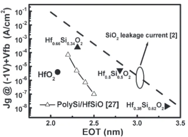
Fig. 8. Relation between leakage current and EOT of the HfO2 and
Hf-silicate devices. The SiO2trend line is also shown (dashed line).
Fig. 9. Dit of HfO2 and Hf-silicate devices with Pt electrodes before
and after PMA. The Dit value of all high-k samples with PMA is below
1012eV−1· cm−2.
is 2.5× 10⁻⁴ cm2. The interfacial chemical oxide is grown by SC-1 before the insulator to restrict the interface trap density. The capacitance of the accumulation region in-creases, indicating an increase in the dielectric constant with increasing Hf concentration (38% to 100%). The gate leakage current density versus EOT of HfxSi1−xO2 at a gate voltage of flatband voltage(VFB)− 1 for an n-channel metal–oxide–semiconductor diode is shown in Fig. 8. The HfO2device shows a 104× leakage current reduction as com-pared to the SiO2device, and the Hf-silicate devices show about one order of magnitude or less leakage current reduction as compared to the SiO2 device. Note that the relatively larger leakage current as compared to [27] may be due to the larger interfacial layer thickness of our silicate samples. The thinner interfacial layer thickness (1 nm in [27]) with the sample EOT (larger physical thickness of the high-k layer) will thus reduce the leakage current [27], [28]. The interface trap density Dit at VFB measured by the high–low (100 and 1 kHz) frequency method is shown in Fig. 9. The Ditof these devices is of the order of 1× 1012cm−2· eV−1without PMA and is reduced by about one order of magnitude after a PMA process. The HfO2 device has the smallest Ditboth after PMA and before PMA, indicating that the Si in Hf-silicate can create interface defects at the HfO2/SiO2interface.
IV. CONCLUSION
In summary, we find that the weak FTIR signal from thin Hf1−xSixO2 films can be detected by using a “face-to-face” structure. When the HfO2 thin film on oxide is annealed at high temperature (600 ◦C and 1000 ◦C), the formation of a Hf-silicate layer in the HfO2/SiO2 interface is evidenced by the occurrence of the FTIR peaks at 960, 900, and 820 cm−1, attributed to Hf–Si–O stretching vibrations. Moreover, XPS results also indicate a great signature of the formation of a Hf-silicate layer. The annealed nanomixed HfO2/SiO2sample has the same FTIR peaks, indicating that the nanomixed HfO2/SiO2 transformed into Hf-silicate after the thermal process.
ACKNOWLEDGMENT
The authors would like to thank Dr. M. Temple for proof-reading this paper.
REFERENCES
[1] International Technology Roadmap for Semiconductors, Semiconductors Industry Association, San Jose, CA, 2001.
[2] Y.-C. Yeo, T.-J. King, and C. Hu, “MOSFET gate leakage modeling and selection guide for alternative gate dielectrics based on leakage consid-erations,” IEEE Trans. Electron Devices, vol. 50, no. 4, pp. 1027–1035, Apr. 2003.
[3] C. Hobbs, H. Tseng, K. Reid, B. Taylor, L. Dip, L. Hebert, R. Garcia, R. Hegde, J. Grant, D. Gilmer, A. Franke, V. Dhandapani, M. Azrak, L. Prabhu, R. Rai, S. Bagchi, J. Conner, S. Backer, F. Dumbuya, B. Nguyen, and P. Tobin, “80 nm poly-Si gate CMOS with HfO2 gate
dielectric,” in IEDM Tech. Dig., 2001, pp. 651–654.
[4] G. D. Wilk, R. M. Wallace, and J. M. Anthony, “High-k gate dielectrics: Current status and materials properties considerations,” J. Appl. Phys., vol. 89, no. 10, pp. 5243–5275, 2001.
[5] R. Choi, C. S. Kang, B. H. Lee, K. Onishi, R. Nieh, S. Gopalan, E. Dharmarajan, and J. C. Lee, “High-quality ultra-thin HfO2gate
dielec-tric MOSFETs with TaN electrode and nitridation surface preparation,” in
VLSI Symp. Tech. Dig., 2001, pp. 15–16.
[6] S. Pidin, Y. Morisaki, Y. Sugita, T. Aoyama, K. Irino, T. Nakamura, and T. Sugii, “Low standby power CMOS with HfO2gate oxide for 100-nm
generation,” in VLSI Symp. Tech. Dig., 2002, pp. 28–29.
[7] R. Chau, S. Datta, M. Doczy, B. Doyle, J. Kavalieros, and M. Metz, “High-κ/metal-gate stack and its MOSFET characteristics,” IEEE
Electron Device Lett., vol. 25, no. 6, pp. 408–410, Jun. 2004.
[8] P. Punchaipetch, G. Pant, M. A. Quevedo-Lopez, C. Yao, M. El-Bouanani, M. J. Kim, R. M. Wallace, and B. E. Gnade, “Low-temperature deposi-tion of hafnium silicate gate dielectrics,” IEEE J. Sel. Topics Quantum
Electron., vol. 10, no. 1, pp. 89–100, Jan./Feb. 2004.
[9] W. Zhu, T. P. Ma, T. Tamagawa, Y. Di, J. Kim, R. Carruthers, M. Gibson, and T. Furukawa, “HfO2and HfAlO for CMOS: Thermal stability and
current transport,” in IEDM Tech. Dig., 2001, pp. 463–466.
[10] M.-Y. Ho, H. Gonga, G. D. Wilk, B. W. Busch, M. L. Green, W. H. Lin, A. See, S. K. Lahiri, M. E. Loomans, P. I. Raisanen, and T. Gustafsson, “Suppressed crystallization of Hf-based gate dielectrics by controlled ad-dition of Al2O3using atomic layer deposition,” Appl. Phys. Lett., vol. 81,
no. 22, pp. 4218–4220, Nov. 2002.
[11] E. Vainonen-Ahlgren, E. Tois, T. Ahlgren, L. Khriachtchev, J. Marles, S. Haukka, and M. Tuominen, “Atomic layer deposition of hafnium and zirconium silicate thin films,” Comput. Mater. Sci., vol. 27, no. 1/2, pp. 65–69, 2003.
[12] D.-S. Kil, K. Hong, K.-J. Lee, J. Kim, H.-S. Song, K.-S. Park, J.-S. Roh, H.-C. Sohn, J.-W. Kim, and S.-W. Park, “Development of highly robust nano-mixed HfxAlyOzdielectrics for TiN/HfxAlyOz/TiN capacitor
ap-plicable to 65 nm generation DRAMs,” in VLSI Symp. Tech. Dig., 2004, pp. 126–127.
[13] T.-H. Moon, M.-H. Ham, M.-S. Kim, I. Yun, and J.-M. Myoung, “Growth and characterization of MOMBE grown HfO2,” Appl. Surf. Sci., vol. 240,
tional, and lattice dielectric properties of hafnium oxide,” Phys. Rev. B., vol. 65, no. 23, p. 233 106, 2002.
[20] M. Ito, K. Kamiya, M. Hori, and T. Goto, “Subsurface reactions of silicon nitride in a highly selective etching process of silicon oxide over silicon nitride,” J. Appl. Phys., vol. 91, no. 5, pp. 3452–3458, 2002.
[21] D. Triyoso, R. Liu, D. Roan, M. Ramon, N. V. Edwards, R. Gregory, D. Werho, J. Kulik, G. Tam, E. Irwin, X.-D. Wang, L. B. La, C. Hobbs, R. Garcia, J. Baker, B. E. White, Jr., and P. Tobin, “Impact of deposition and annealing temperature on material and electrical characteristics of ALD HfO2,” J. Electrochem. Soc., vol. 151, no. 10, pp. F220–F227, 2004.
[22] C. C. Yeo, M. S. Joo, B. J. Cho, and S. J. Whang, “Effect of annealing on the composition and structure of HfO2and nitrogen-incorporated HfO2,” Thin Solid Films, vol. 462/463, pp. 90–95, 2004.
[23] M.-H. Cho, K. B. Chung, C. N. Whang, D. W. Lee, and D.-H. Ko, “Phase separation and electronic structure of Hf-silicate film as a function of composition,” Appl. Phys. Lett., vol. 87, no. 24, p. 242 906, 2005. [24] R. Ludeke and E. Gusev, “Structural and surface potential characterization
of annealed HfO2and (HfO2)x(SiO2)1−xfilms,” J. Appl. Phys., vol. 96, no. 4, pp. 2365–2373, 2004.
[25] P. S. Lysaght, P. J. Chen, R. Bergmann, T. Messina, R. W. Mutro, and H. R. Huff, “Experimental observations of the thermal stability of high-k gate dielectric materials on silicon,” J. Non-Cryst. Solids, vol. 303, no. 1, pp. 54–63, May 2002.
[26] P.-J. Tzeng, S. Maikap, P.-S. Chen, Y.-W. Chou, C.-S. Liang, and L.-S. Lee, “Physical and reliability characteristics of Hf-based gate dielectrics on strained-Si1−xGexMOS devices,” IEEE Trans. Device Mater. Rel.,
vol. 5, no. 2, pp. 168–176, Jun. 2005.
[27] A. Morioka, H. Watanabe, M. Miyamura, T. Tatsumi, M. Saitoh, T. Ogura, T. Iwamoto, T. Ikarashi, Y. Saito, Y. Okada, H. Watanabe, Y. Mochiduki, and T. Mogami, “High mobility MISFET with low trapped charge in HfSiO films,” in VLSI Symp. Tech. Dig., 2003, pp. 165–166.
[28] Y. Y. Fan, Q. Xiang, J. An, L. F. Register, and S. K. Banerjee, “Impact of interfacial layer and transition region on gate current performance for high-k gate dielectric stack: Its tradeoff with gate capacitance,” IEEE
Trans. Electron Devices, vol. 50, no. 2, pp. 433–439, Feb. 2003.
Tze Chiang Chen received the B.S. and M.S.
de-grees in electrical engineering from Chang Gung University, Tao-Yuan, Taiwan, R.O.C., in 1999 and 2001, respectively, and the Ph.D. degree from the National Taiwan University (NTU), Taipei, Taiwan, R.O.C., in 2006.
He is currently with the Department of Electri-cal Engineering and Graduate Institute of Electron-ics Engineering, NTU. His research interests are in high-k material, visible light from quantum dots device, and interface properties of semiconductors by MOS tunneling light-emitting diodes.
R.O.C., in 2004 and 2006, respectively.
He is currently with the Department of Electrical Engineering and Graduate Institute of Electronics Engineering, NTU. His research interests include strained Si devices and Schottky barrier MOSFETs.
Ming-Han Liao (S’04) received the B.S. degree in
mechanical engineering from the National Taiwan University (NTU), Taipei, Taiwan, R.O.C., in 2002.
Since 2002, he has been with the advanced silicon process group at the Department of Electrical En-gineering and Graduate Institute of Electro-Optical Engineering, NTU, where he has been involved in strained Si technology and SiGe-based photonics. He has authored or coauthored more than 30 pub-lications/presentations and has three International Electron Device Meeting papers.
Mr. Liao received the Zhuo Zhang-Zong Scholarship Award in 2005 for his outstanding research work.
Mei-Hsin Chen received the B.S. and M.S. degrees
in electrophysics from the National Chiao Tung Uni-versity, Hsinchu, Taiwan, R.O.C., in 2001 and 2004, respectively. She is currently working toward the Ph.D. degree at the Department of Electrical En-gineering and Graduate Institute of Electro-Optical Engineering, National Taiwan University, Taipei, Taiwan, R.O.C.
Her current research interests include electron-injection mechanisms and interfacial chemical reac-tion in organic light-emitting devices.
Chih-I Wu received the B.S. degree in physics
from the National Taiwan University (NTU), Taipei, Taiwan, R.O.C., the M.S. degree in physics from Northwestern University, Evanston, IL, and the Ph.D. degree in electrical engineering from Prince-ton University, PrincePrince-ton, NJ, in 2000.
He was with the Component Research Divi-sion, Intel Corporation from 2000 to 2004 and was involved in developing advanced semiconductor process technology. He is currently an Associate Professor at the Department of Electrical Engineer-ing and Graduate Institute of Electro-Optical EngineerEngineer-ing, NTU. His research interests include organic materials for light-emitting diodes, interface proper-ties of semiconductors, and advanced interconnects and gate stack for nano-scaled CMOS.
766 IEEE TRANSACTIONS ON ELECTRON DEVICES, VOL. 54, NO. 4, APRIL 2007
Ming-Yau Chern received the B.S. degree in
physics from the National Taiwan University (NTU), Taipei, Taiwan, R.O.C., in 1984 and the Ph.D. degree in physics from Cornell University, Ithaca, NY, in 1991.
He is currently a Professor of Physics at the Department of Physics, NTU. His research interests are in the synthesis of thin film materials, X-ray crystallography, ellipsometry, transparent conduct-ing oxides, and new nitrides.
Pei-Jer Tzeng (M’03) received the Ph.D. degree in
engineering and system science from the National Tsing Hua University, Hsinchu, Taiwan, R.O.C., in 2002.
He is currently with the Electronics Research and Service Organization, Industrial Technology Research Institute, Hsinchu. His current research in-terests include the fabrication and characterization of MOS devices, gate dielectrics, high-k material, and their application in DRAM and nonvolatile memory.
Chee Wee Liu (M’99–SM’00) received the B.S.
and M.S. degrees in electrical engineering from the National Taiwan University (NTU), Taipei, Taiwan, R.O.C., in 1985 and 1987, respectively, and the Ph.D. degree in electrical engineering from Princeton University, Princeton, NJ, in 1994.
He is currently a Professor at the Department of Electrical Engineering, Graduate Institute of Electronics Engineering, and Graduate Institute of Electro-Optical Engineering, NTU. His current re-search interests include strained Si/Ge, SiGe pho-tonics, Ge/Si on anything, high-k, and metal gate. He invented the first MOS tunneling light-emitting diode/laser diode and photodetectors.