Water passivation effect on polycrystalline silicon nanowires
Horng-Chih Lin, Chun-Jung Su, Cheng-Yun Hsiao, Yuh-Shyong Yang, and Tiao-Yuan Huang
Citation: Applied Physics Letters 91, 202113 (2007); doi: 10.1063/1.2814033 View online: http://dx.doi.org/10.1063/1.2814033
View Table of Contents: http://scitation.aip.org/content/aip/journal/apl/91/20?ver=pdfcov Published by the AIP Publishing
Articles you may be interested in
Hydrogen passivation of polycrystalline silicon thin films J. Appl. Phys. 112, 063711 (2012); 10.1063/1.4752268
Prediction of surface passivation doping of silicon nanowires with phosphorus Appl. Phys. Lett. 95, 193105 (2009); 10.1063/1.3250162
Passivation effects on ZnO nanowire field effect transistors under oxygen, ambient, and vacuum environments Appl. Phys. Lett. 92, 263109 (2008); 10.1063/1.2955512
Mobility enhancement of polycrystalline-Si thin-film transistors using nanowire channels by pattern-dependent metal-induced lateral crystallization
Appl. Phys. Lett. 87, 143504 (2005); 10.1063/1.2076436
High-performance polycrystalline silicon thin-film transistor with multiple nanowire channels and lightly doped drain structure
Appl. Phys. Lett. 84, 3822 (2004); 10.1063/1.1745104
This article is copyrighted as indicated in the article. Reuse of AIP content is subject to the terms at: http://scitation.aip.org/termsconditions. Downloaded to IP: 140.113.38.11 On: Thu, 01 May 2014 00:04:35
Water passivation effect on polycrystalline silicon nanowires
Horng-Chih Lina兲
Institute of Electronics, National Chiao Tung University, Hsinchu 300, Taiwan and National Nano Device Laboratories, Hsinchu 300, Taiwan
Chun-Jung Su
Institute of Electronics, National Chiao Tung University, Hsinchu 300, Taiwan
Cheng-Yun Hsiao and Yuh-Shyong Yang
Institute of Biological Science and Technology, National Chiao Tung University, Hsinchu 300, Taiwan
Tiao-Yuan Huang
Institute of Electronics, National Chiao Tung University, Hsinchu 300, Taiwan
共Received 3 July 2007; accepted 28 October 2007; published online 16 November 2007兲
Defects present in the grain boundaries of polycrystalline materials are known to impede carrier transport inside the materials, and the electronic device performance having such materials as active channels will be adversely affected. In this work, dramatic improvement in device performance was observed as field-effect transistors with polycrystalline silicon nanowire共poly-SiNW兲 channels were exposed to a wet environment. Passivation of defects in the poly-SiNW by H+and/or OH−contained
in the aqueous solution is proposed to explain the phenomenon. © 2007 American Institute of
Physics. 关DOI:10.1063/1.2814033兴
Field-effect transistors 共FETs兲 have been proposed for chemical sensor applications since 1975 by Lundstrom et al. who reported a hydrogen-sensitive FETs with palladium as gate metal.1 In addition to gas detection, FETs can also be used to measure pH or ions in aqueous solutions.2In those early works, the test devices adopted a planar structure hav-ing a channel exposed to the environment. However, the sen-sitivity is seriously affected by the leakage current from source to drain through the bulk of the substrate. To address this issue, recently a sensing structure utilizing Si nanowire 共SiNW兲 as the channel was proposed.3
Owing to the high surface-to-volume ratio, the bulk leakage could be effec-tively suppressed and, thus, the sensitivity is greatly im-proved. Such SiNW sensors have demonstrated their func-tion in detecting protein,3 DNA,4glucose,5and virus.6
The aforementioned works on biological sensing appli-cations employed monocrystalline SiNWs as the channel, en-abling a high carrier mobility which is essential for good device performance. Recently, we investigated the use of polycrystalline silicon 共poly-Si兲 NW channels for building electronic devices.7,8The scheme we proposed could greatly simplify the fabrication flow. However, defects contained in the grain boundaries of the poly-Si NW would impede car-rier transport and thus degrade the mobility.9 For biological sensors, the polycrystalline nature of NWs raises the concern of sensitivity degradation. In this work, we show that such concern could be lifted as long as the measurement is carried out in an aqueous solution.
Here, we briefly describe the fabrication of the poly-Si NW devices. A thermal oxide of 100 nm was first grown on a silicon wafer. Then a 90-nm-thick amorphous silicon film was deposited on the wafer using a low-pressure chemical vapor deposition system. After doping of source/drain共S/D兲 regions using ion implantation technique, the film was then transformed into polycrystalline via an annealing step
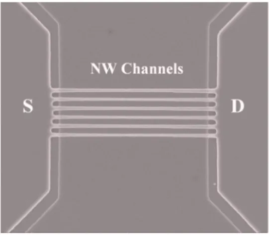
per-formed at 600 ° C in nitrogen ambient. The SiNW channels and S/D regions were patterned simultaneously using e-beam lithography and subsequent plasma dry-etch step. Figure 1
shows the scanning electron microscopic共SEM兲 picture of a device, which contains six NW channels. Afterwards, a pas-sivation oxide was capped on the wafer surface. The SiNW channels were then exposed by removing the covering oxide, and the entire device was then enclosed in a microfluid sample delivery structure with an aim of performing electri-cal measurements in an aqueous environment. During the measurements the Si substrate itself serves as the gate elec-trode upon which a bias is applied to modulate the drain current.
Typical characteristics of the NW transistors at room temperature are shown in Fig.2. First, the measurement was carried out in a dry ambient. Afterwards, de-ionized 共DI兲 water was injected and flowed through the microfluid cavity to immerse the NW channels, and then the same measure-ment scheme was repeated. Detailed performance parameters are summarized in TableI. Two distinct features are found.
a兲Electronic mail: hclin@faculty.nctu.edu.tw FIG. 1. SEM picture of a device which contains six NW channels. Planarwidth and thickness of each NW is 70 and 90 nm, respectively. APPLIED PHYSICS LETTERS 91, 202113共2007兲
0003-6951/2007/91共20兲/202113/3/$23.00 91, 202113-1 © 2007 American Institute of Physics
This article is copyrighted as indicated in the article. Reuse of AIP content is subject to the terms at: http://scitation.aip.org/termsconditions. Downloaded to IP: 140.113.38.11 On: Thu, 01 May 2014 00:04:35
First, the subthreshold swing 共SS兲 dramatically reduces as the measurement environment becomes wet. Note that the very large SS value recorded in the dry ambient is consistent with the fact that the polycrystalline material used in this study contains a large amount of defects. These defects act as trapping centers for carriers9 and tend to slow down the modulation of channel surface potential with increasing gate voltage. Dramatic reduction in SS of the device when oper-ating in a wet environment implies that those trapping sites become ineffective. The other important finding is the sig-nificant increase in mobility and the saturation drain current when measured in a wet environment. This again evidences the decrease in the amount of active defects in the channels, which is further confirmed by extracting the trap density 共Table I兲 using the Levinson method.10 These differences originating from the different measurement environments imply that the ingredients contained in the water play an essential role in modifying the conduction behavior of carri-ers inside the NW. It is worth noting that when measured in a wet environment, the performance of poly-Si NW devices is almost on a par with that of monocrystalline-Si NW devices.11
Passivation of defects in poly-Si by hydrogen-related species is well-known and has been utilized extensively for improving the device performance of poly-Si thin-film tran-sistors共TFTs兲. Such treatment is typically done by exposing the devices to an H-containing plasma12 or via a high-pressure water vapor annealing step.13 Since the TFTs are
normally capped with a dielectric 共typically a silicon oxide layer兲, these process treatments are usually performed at an elevated temperature to enhance the passivation mechanisms. Among the previously developed techniques, the process ambient of high-pressure vapor anneal contains same ingre-dients as the wet environment investigated in this work. So we postulate that similar mechanism may occur in our de-vices. The DI water is neutral with pH value of 7. This means that the concentration of H+ 共and OH−兲 is
10−7mole/ L or 6.02⫻1013 cm−3. This value is actually
much higher than ion density in typical H-containing plas-mas共⬃1010cm−3兲.12The abundant H+and/or OH−may dif-fuse into the grain boundaries and terminate on the dangling bonds wherein. As a consequence, the amount of electrically active defects is substantially reduced, resulting in a dramatic improvement of device performance.
To test the reproducibility of the water passivation effect, measurements were repeatedly performed on a device which went through seven stages of exposure to alternate dry and wet environments. Within each stage the device was charac-terized several times to confirm the stability of device per-formance, and the representative I-V curves for all stages are shown in Fig. 3. Clearly, the device characteristics recover when the device was switched from wet to dry environment and vice versa. Also worth noting in this figure is that the passivation effect occurs only in water, indicating that the passivation bonds are not stable and could easily be desorbed from the poly-Si NW when the water is pumped away from the microfluid cavity.
The significance of the water passivation effect found in this work is that it can be cleverly used to boost the perfor-mance of poly-Si NW devices to a level comparable to the monocrystalline counterparts.11This scheme is thus suitable for biologic sensing applications, which are usually done in aqueous solutions. Since poly-Si is easier to grow and pre-pare on a number types of substrates, this finding is attractive for biological sensing device fabrication in terms of lower complexity as well as reduced cost.
This work was supported in part by the National Science Council of the Republic of China under Contract No. NSC 95-2221-E-009-297.
FIG. 2. Transfer characteristics of a device operating in dry and wet共DI water, denoted as DIW兲 environments.
TABLE I. Comparisons of device performance parameters measured in dry and wet共DI water兲 environments.
Ambient Dry Wet
Threshold voltage共V兲 6.8 0.7
Mobilitya共cm2/ V sec兲 75 126
Subthreshold swing共V/decade兲 1.1 0.2
Trap densityb共1012cm−2兲 1.2 0.41
aThe channel width used in mobility extraction procedure is 70 nm 共the
planar width of the SiNW兲 for the case of dry ambient. However, owing to the high dielectric constant of water 共⬃80兲, a gate-all-around operation scheme is assumed for the case of wet ambient. In other words, the effective width is assumed to be 320 nm共the total edge length of the NW’s cross section兲 for the case of wet ambient.
bTrap density was extracted using the method presented in Ref.10.
FIG. 3. Transfer characteristics of a device operating in seven stages of alternative dry and wet environments. Period of each stage is about 14 min.
202113-2 Lin et al. Appl. Phys. Lett. 91, 202113共2007兲
This article is copyrighted as indicated in the article. Reuse of AIP content is subject to the terms at: http://scitation.aip.org/termsconditions. Downloaded to IP: 140.113.38.11 On: Thu, 01 May 2014 00:04:35
1I. Lundstrom, M. S. Shivaraman, and C. M. Svensson, J. Appl. Phys. 46,
3876共1975兲.
2P. Bergveld, IEEE Trans. Biomed. Eng. 17, 70共1990兲.
3Y. Cui, Z. Wei, H. Park, and C. M. Lieber, Science 293, 1289共2001兲. 4Z. Li, Y. Chen, X. Li, T. I. Kamins, K. Nauka, and R. S. Williams, Nano
Lett. 4, 245共2004兲.
5W. Chen, H. Yao, C. H. Tzang, J. Zhu, M. Yang, and S. T. Lee, Appl.
Phys. Lett. 88, 213104共2006兲.
6F. Patolsky and C. M. Lieber, Mater. Today 8, 20共2005兲.
7H. C. Lin, M. H. Lee, C. J. Su, T. Y. Huang, and Y. S. Huang, IEEE
Electron Device Lett. 26, 643共2005兲.
8H. C. Lin, M. H. Lee, C. J. Su, and S. W. Shen, IEEE Trans. Electron
Devices 53, 2471共2006兲.
9J. Y. W. Seto, J. Appl. Phys. 46, 5247共1975兲.
10J. Levinson, F. R. Shepherd, P. J. Scanlon, W. D. Westood, G. Este, and M.
Rider, J. Appl. Phys. 53, 1193共1982兲.
11Y. Cui, Z. Zhong, D. Wang, W. U. Wang, and C. M. Lieber, Nano Lett. 3,
149共2003兲.
12M. Yu, H. C. Lin, K. L. Yeh, T. Y. Huang, and T. F. Lei, J. Electrochem.
Soc. 150, G843共2004兲.
13U. Mira, J. Chen, B. Khan, and E. Stupp, IEEE Electron Device Lett. 12,
390共1991兲.
202113-3 Lin et al. Appl. Phys. Lett. 91, 202113共2007兲
This article is copyrighted as indicated in the article. Reuse of AIP content is subject to the terms at: http://scitation.aip.org/termsconditions. Downloaded to IP: 140.113.38.11 On: Thu, 01 May 2014 00:04:35