Stable inverted bottom-emitting organic electroluminescent devices with molecular
doping and morphology improvement
Szu-Yi Chen, Ta-Ya Chu, Jenn-Fang Chen, Chien-Ying Su, and Chin H. Chen
Citation: Applied Physics Letters 89, 053518 (2006); doi: 10.1063/1.2335374 View online: http://dx.doi.org/10.1063/1.2335374
View Table of Contents: http://scitation.aip.org/content/aip/journal/apl/89/5?ver=pdfcov Published by the AIP Publishing
Articles you may be interested in
Improvement of electron injection in inverted bottom-emission blue phosphorescent organic light emitting diodes using zinc oxide nanoparticles
Appl. Phys. Lett. 96, 153306 (2010); 10.1063/1.3400224
Cesium hydroxide doped tris-(8-hydroxyquinoline) aluminum as an effective electron injection layer in inverted bottom-emission organic light emitting diodes
Appl. Phys. Lett. 92, 263305 (2008); 10.1063/1.2955516
Improved electroluminescent efficiency of organic light emitting devices by co-doping N, N -Dimethyl-quinacridone and Coumarin6 in tris-(8-hydroxyquinoline) aluminum
Appl. Phys. Lett. 87, 213501 (2005); 10.1063/1.2132064
The effect of C60 doping on the device performance of organic light-emitting diodes Appl. Phys. Lett. 86, 063514 (2005); 10.1063/1.1861962
Efficient bottom cathodes for organic light-emitting devices Appl. Phys. Lett. 85, 837 (2004); 10.1063/1.1776620
This article is copyrighted as indicated in the article. Reuse of AIP content is subject to the terms at: http://scitation.aip.org/termsconditions. Downloaded to IP: 140.113.38.11 On: Thu, 01 May 2014 01:53:01
Stable inverted bottom-emitting organic electroluminescent devices with
molecular doping and morphology improvement
Szu-Yi Chen
Display Institute, National Chiao Tung University, Hsinchu, Taiwan 300, Republic of China
Ta-Ya Chua兲and Jenn-Fang Chen
Institute of Electrophysics, National Chiao Tung University, Hsinchu, Taiwan 300, Republic of China
Chien-Ying Su
Instrument Technology Research Center, National Applied Research Laboratories, Hsinchu, Taiwan 300, Republic of China
Chin H. Chen
Display Institute, National Chiao Tung University, Hsinchu, Taiwan 300, Republic of China and Microelectronics and Information Systems Research Center, National Chiao Tung University, Hsinchu Taiwan 300, Republic of China
共Received 29 April 2006; accepted 30 June 2006; published online 4 August 2006兲
Stable inverted bottom-emitting organic light-emitting diodes共IBOLEDs兲 have been investigated by inserting n-type Cs2O dopant between indium-tin oxide bottom cathode and Alq3, the combination
of which not only improved the morphology of organic layer but enhanced the lifetime of the IBOLED. This n-type doped IBOLED achieved efficiencies of 5.2 cd/ A and 2.0 lm/ W at 20 mA/ cm2. The 20% decay lifetime 共t80兲 of Cs2O doped IBOLED is 270 h which is about 1.7
times more stable than that of the conventional OLED共160 h兲 and 2.5 times of Li doped IBOLED 共104 h兲. © 2006 American Institute of Physics. 关DOI:10.1063/1.2335374兴
Organic light-emitting devices 共OLEDs兲 have been de-veloped for many years emerging as one of the main con-tenders of the next-generation information flat displays. Typical OLEDs have a transparent electrode indium-tin ox-ide 共ITO兲 with high work function deposited on glass for anode and have an opaque metal for cathode such as Mg: Ag 共Ref. 1兲 and Al/LiF 共Ref. 2兲 from which light is reflected and emitted through the bottom ITO glass. To take advantage of the n-channel a-Si thin film transistor共TFT兲 which gives better uniform brightness for large display, it is highly desir-able for active-matrix organic light-emitting diode 共AMOLED兲 to employ an inverted OLED 共IOLED兲 device which has the inverted structure with the bottom contact as the cathode. There have been several inverted top-emitting OLEDs共ITOLEDs兲 reported in the literature which need a reflective cathode as the base substrate and a transparent ITO sputtered above the organic layers as anode. However, the intense radiation energy created by sputtering would damage the organic layer and induce more nonradiactive relaxation of the injected carriers3,4 The inverted bottom-emitting OLED共IBOLED兲 on the other hand is free from such prob-lem. As a result, IBOLED will likely become more important in the future, particularly for large AMOLED displays such as future TV applications where large sized a-Si TFT is readily available and free from uniformity problems of the rival low temperature polysilicon TFT. Usually, structure of IBOLED has an ITO bottom cathode and an opaque and reflective top metal as anode to allow light to escape from ITO glass at the bottom. Since the transparent ITO has a high work function, efficient electron injection from ITO into or-ganic has been a dogged issue to be resolved in IBOLED. We had proposed earlier that the barrier between ITO and
Alq3 can be reduced by interfacial charge-transfer dipole by
evaporating an ultrathin layer of magnesium共Mg兲 onto ITO which produced IBOLED with a luminous and current effi-ciencies of 1.51 lm/ W and 4.66 cd/ A, respectively, at a driving voltage of 8.9 V and current density of 20 mA/ cm2.5
It has also been reported that doping can increase the mobility of carriers and lead to generation of very thin space-charge layers at the contacts associated with efficient injection.6–8 For examples, Zhou et al. had reported n-i-p structure using Li doping in transparent inverted OLED共Ref. 9兲 to reduce drive voltage. However, the small atom of Li is prone to diffuse into organic layer which can cause nonra-dioative recombination10–12 and ultimately leads to reduced device stability. In previous studies, the small atom of Li has been replaced by the larger atom of Cs to serve as the n-type dopant.13But, pure, low melting Cs source is rather difficult to handle and deposit by thermal process because it is ex-tremely reactive in air. Often a specially designed and expen-sive Cs dispenser is needed to accomplish the trick in a vacuum chamber. Therefore, there is a continuing need to develop molecular n dopant for OLED. In this letter, we report the molecular Cs2O doping to enhance electron
injec-tion in IBOLED. Addiinjec-tionally, this Cs2O dopant will also
improve the morphology of the electron injection layer with which significantly enhanced lifetime can be achieved.
In our study, the thickness and sheet resistance of ITO glass were 100 nm and 35⍀/䊐, respectively. Prior to depo-sition, the ITO coated glass substrates were sequentially cleaned in acetone, isopropyl alcohol, and de-ionized water and these materials were then deposited by thermal evapora-tion in an ULVAC Solciet OLED coater at a vacuum of 10−7torr. n doping of Cs
2O decomposed by cesium
carbon-ate 共Cs2CO3兲 can be easily handled in the fabrication
processes.14 Further, Wakimoto et al.15 has reported that
a兲Electronic mail: [email protected]
APPLIED PHYSICS LETTERS 89, 053518共2006兲
0003-6951/2006/89共5兲/053518/3/$23.00 89, 053518-1 © 2006 American Institute of Physics
This article is copyrighted as indicated in the article. Reuse of AIP content is subject to the terms at: http://scitation.aip.org/termsconditions. Downloaded to IP: 140.113.38.11 On: Thu, 01 May 2014 01:53:01
Cs2CO3will decomposed into Cs2O according to the
follow-ing reaction:
Cs2CO3+ heat→ Cs2O + CO2.
But, recently, Wu et al. reported that Cs2CO3 deposited on the Au substrate measured with x-ray photoemission spectra 共XPS兲 found that Cs2CO3 did not decompose during the
evaporation.16However, contrary to the observation of Wu et
al., we found that during thermal evaporation, the pressure in
the vacuum chamber had increased rapidly near the decom-position temperature of Cs2CO3which we believe was due to
the formation of Cs2O and gaseous CO2. The transition metal
oxides, such as V2O5,17MoO3,18and WO3共Refs. 19 and 20兲
have been used to enhance the hole injection in the litera-tures. We opted to use WO3 as the hole-injection layer. The OLED structures of the conventional OLED and IBOLED are shown in Fig. 1, ITO/ CuPc/ NPB/ Alq3/ LiF / Al 共device
A兲, ITO/Cs2O : Bphen/ / Alq3/ NPB/ WO3/ Al 共device B兲,
and ITO/ Li: Bphen/ Alq3/ NPB/ WO3/ Al 共device C兲, and designated as Figs. 1共a兲–1共c兲, respectively. The current-density–voltage-luminance共J-V-L兲 characteristics of the de-vices were measured by using a Photo Research PR650 spec-trophotometer and a computer-controlled programmable dc source 共Keithley 2400兲. Atomic force microscopy 共AFM兲 was used in an attempt to correlate these characteristics of the surface morphology. The lifetime was measured in a glove box at a constant driving current density of 20 mA/ cm2.
The dependency of the voltage on current density and luminance is shown in Fig. 2. We find at the same current density that the performance of the Cs2O doped IBOLED is comparable with that of the conventional OLED in bright-ness, but its voltage is lower with 8.32, 8.15, and 9.62 V at 20 mA/ cm2 for devices A–C, respectively. The maximum
brightness of Cs2O-doping device achieved 22 061 cd/ m2at
450 mA/ cm2. Wu et al.16
has found that there were extra states above the Alq3 highest occupied molecular orbital
when Alq3 was doped with Cs2CO3. We would like to
pro-pose instead that Cs2O-doping Bphen layer between ITO and
Alq3 could provide certain trap states which would enhance electron injections from ITO to the Alq3. Table I summarizes the performance of the devices at a drive current density of 20 mA/ cm2. In previous studies, Cs atom which is larger
than Li has been exploited as the n dopant to reduce the probability of metal diffusing into emission layer and quenching the excitons.21We propose that molecular Cs2O is
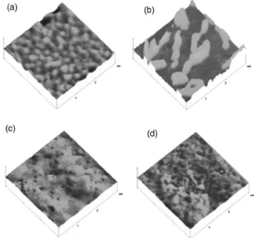
even better for alleviating the problem of diffusion into or-ganic layer which causes nonradioative recombination. Fur-thermore, the electron-transporting Bphen which is known to be morphologically unstable has been found to induce device degradation.22Figure 3 shows the AFM surface morphology of films deposited on glass substrates with the same thick-ness. The average surface roughnesses 共root mean square average兲 are 4.3, 18.9, 2.94, and 2.3 nm for Bphen without or with annealing and Cs2O doped Bphen without or with annealing, respectively共Fig. 3兲. Compare Fig. 3共a兲 with 3共b兲,
FIG. 1. Structure of inverted bottom-emitting OLED and conventional OLED.
FIG. 2. Current-density–voltage-luminance characteristics of ITO/ CuPc/ NPB/ Alq3/ LiF / Al 共device A兲, ITO/ Cs2O : Bphen/ Alq3/ NPB/ WO3/ Al 共device B兲, and ITO/ Li: Bphen/ Alq3/ NPB/ WO3 / Al共device C兲.
TABLE I. Characteristic performances of the inverted bottom-emitting OLED共IBOLED兲 and conventional OLED driven at 20 mA/cm2.
Device Voltage 共V兲 Brightness 共cd/m2兲 Lum. yield 共cd/A兲 Power efficiency 共lm/W兲 A 8.32 1106 5.53 2.09 B 8.15 1038 5.19 2.00 C 9.60 1078 5.39 1.85
FIG. 3. Surface morphology of Bphen and Cs2O doped Bphen by AMF.共a兲 Bphen without anneal,共b兲 Bphen with annealing, 共c兲 Cs2O doped Bphen without annealing, and共d兲 Cs2O doped Bphen with annealing.
053518-2 Chen et al. Appl. Phys. Lett. 89, 053518共2006兲
This article is copyrighted as indicated in the article. Reuse of AIP content is subject to the terms at: http://scitation.aip.org/termsconditions. Downloaded to IP: 140.113.38.11 On: Thu, 01 May 2014 01:53:01
crystallization is evident in Bphen films after annealing at 80 ° C for 20 min. However, by doping Bphen film with Cs2O, the phenomenon of crystallization after annealing
un-der the same condition is clearly suppressed. We expect therefore that the Cs2O doped Bphen should improve device
operational stability under thermal stress.
Figure 4 shows the lifetime for IBOLED in comparison with the conventional OLED which was measured in a glove box at a constant drive current density of 20 mA/ cm2.
Al-though the efficiencies of Li doped device can reach 5.39 cd/ A and 1.85 lm/ W, its lifetime was rather short due to the diffusion of the Li atom. On the other hand, the Cs2O
doping of IBOLED device is observed to have much longer lifetime than both the convention OLED and Li doping of IBOLED devices with the t80of devices A–C 160, 270, and 104 h, respectively, at a constant current density of 20 mA/ cm2.
To conclude, Cs2O doping of IBOLED has excellent
per-formance, including high efficiency, low voltage, and long lifetime. We suggest that thin Cs2O doped Bphen layer can provide trap states to enhance electron injection. In addition, the molecular Cs2O will eliminate the diffusion of Cs atom
into the organic layer to create the nonradiative recombina-tion. We also find that Cs2O doped Bphen layer has good
morphological stability which is likely to reduce nonemis-sive dark spot growth. As a result, Cs2O doped IBOLED is
1.7 times more stable than the conventional OLED and 2.5 times than Li doping of IBOLED at the 20% decay lifetime 共t80兲.
This work was supported by a grant from Chunghwa Picture Tubes, Ltd.共CPT兲 of Taoyuan, Taiwan, that also pro-vides scholarship for two of the authors 共S.-Y.C.兲 and 共T.-Y.C.兲 to pursue their advanced studies at NCTU.
1C. W. Tang and S. A. V. Slyke, J. Appl. Phys. 65, 3610共1989兲. 2L. S. Hung, C. W. Tang, and M. G. Mason, Appl. Phys. Lett. 70, 152
共1997兲.
3L. S. Liao, L. S. Hung, W. C. Chan, X. M. Ding, T. K. Sham, I. Bello, C. S. Lee, and S. T. Lee, Appl. Phys. Lett. 75, 1619共1999兲.
4G. Parthasarathu, P. E. Burrows, V. Khalfin, V. G. Kozlov, and S. R. Forrest, Appl. Phys. Lett. 72, 2138共1998兲.
5T.-Y. Chu, S.-Y. Chen, J.-F. Chen, and C. H. Chen, Jpn. J. Appl. Phys. 45, 4948共2006兲.
6A. Werner, K. Harada, M. Pfeiffer, L. Fritz, K. Leo, and S. Machill, Adv. Funct. Mater. 14, 255共2004兲.
7J. Huang, M. Pfeiffer, A. Werner, J. Blochwitz, and K. Leo, Appl. Phys. Lett. 80, 139共2002兲.
8G. He, M. Pfeiffer, and K. Leo, Appl. Phys. Lett. 85, 3911共2004兲. 9X. Zhou, M. Pfeiffer, J. S. Huang, J. Blochwitz-Nimoth, D. S. Qin, A.
Werner, J. Drechsel, B. Maening, and K. Leo, Appl. Phys. Lett. 81, 922 共2002兲.
10G. Parthasarathy, C. Shen, A. Kahn, and S. R. Forrest, J. Appl. Phys. 89, 4986共2001兲.
11E. I. Haskal, A. Curioni, and P. F. Seidler, Appl. Phys. Lett. 71, 1151 共1997兲.
12V. Choong, Y. Park, Y. Gao, T. Wehrmeister, K. Müllen, B. R. Hsieh, and C. W. Tang, Appl. Phys. Lett. 69, 1492共1996兲.
13J.-H. Lee, M.-H. Wu, C.-C. Chao, H.-L. Chen, and M.-K. Leung, Chem. Phys. Lett. 416, 234共2005兲.
14T. Hasegawa, S. Miura, T. Moriyama, T. Kimura, I. Takaya, Y. Osato, and H. Mizutani, SID Proceedings, 2004, p. 154.
15T. Wakimoto, Y. Fukuda, K. Nagayama, A. Yokoi, H. Nakada, and M. Tsuchida, IEEE Trans. Electron Devices 44, 1245共1997兲.
16C.-I. Wu, C.-T. Lin, Y.-H. Chen, M.-H. Chen, Y.-J. Lu, and C.-C. Wu, Appl. Phys. Lett. 88, 152104共2006兲.
17C.-W. Chu, C.-W. Chen, S.-H. Li, H.-E. Wu, and Y. Yang, Appl. Phys. Lett. 86, 253503共2005兲.
18T. Miyashita, S. Naka, H. Okada, and H. Onnagawa, IDW Proceedings, 2004, p. 1421.
19J. Li, M. Yahiro, K. Ishida, H. Yamada, and K. Matsushige, Synth. Met. 151, 141共2005兲.
20C.-C. Chang, M.-T. Hsieh, J.-F. Chen, S.-W. Hwang, J.-W. Ma, and C. H. Chen, SID Proceedings, 2006, p. 1106.
21G. He, O. Schneider, D. Qin, X. Zhou, M. Pfeiffer, and K. Leo, J. Appl. Phys. 95, 5773共2004兲.
22B. W. D’Andrade, S. R. Forrest, and A. B. Chwang, Appl. Phys. Lett. 83, 3858共2003兲.
FIG. 4. Lifetime of ITO/ CuPc/ NPB/ Alq3/ LiF / Al 共device A兲, ITO/ Cs2O : Bphen/ Alq3/ NPB/ WO3/ Al 共device B兲, and ITO/ Li: Bphen/ Alq3/ NPB/ WO3 / Al共device C兲.
053518-3 Chen et al. Appl. Phys. Lett. 89, 053518共2006兲
This article is copyrighted as indicated in the article. Reuse of AIP content is subject to the terms at: http://scitation.aip.org/termsconditions. Downloaded to IP: 140.113.38.11 On: Thu, 01 May 2014 01:53:01