低溫陶瓷共燒平衡式頻率雙工器模組
53
0
0
全文
(2) 低溫陶瓷共燒平衡式頻率雙工器模組 The Low Temperature Cofired Ceramic Balanced Diplexer Module. 研 究 生:余思嫻 指導教授:張志揚 博士. Student:Szu-Hsien Yu Advisor:Dr. Chi-Yang Chang. 國立交通大學 電信工程學系 碩士論文. A Thesis Submitted to Institute of Communication Engineering College of Electrical Engineering and Computer Science National Chiao Tung University In Partial Fulfillment of the Requirements for the Degree of Master of Science In Communication Engineering June 2005 Hsinchu, Taiwan, Republic of China 中華民國 九十四 年 六 月 -2-.
(3) 低溫陶瓷共燒平衡式頻率雙工器模組 研究生:余思嫻. 指導教授:張志揚 博士. 國立交通大學電信工程學系. 摘要. 在本論文中,利用高介電係數( ε r = 33 )及低損耗性的低溫共燒 陶瓷材料,設計小尺寸及低損耗的平衡式頻率雙工器模組。此低溫 共燒陶瓷平衡式頻率雙工器模組包含雙工器、帶通濾波器、低通濾 波器、平衡轉換器,並符合 IEEE 802.11a (5.2GHz、5.7GHz)與 802.11b (2.4 GHz)無線區域網路系統的規格要求。在此,我們利用 m-derived 基本原理設計低通濾波器,帶通濾波器則是使用三階交錯耦合架 構,使得低頻訊號、二倍頻和三倍頻訊號有較佳的抑制效果。最後, 利用傳輸線連接低通和帶通濾波器設計雙工器,並且連接帶通濾波 器和平衡轉換器,以完成模組設計。. i.
(4) The Low Temperature Cofired Ceramic Balanced Diplexer Module Student: Szu-Hsien Yu. Advisor: Dr. Chi-Yang Chang. Institute of Communication Engineering National Chiao Tung University. Abstract. This thesis presents a small-size and low-insertion-loss balanced diplexer module by using LTCC technique. This module comprises two diplexers, five bandpass filters, a lowpass filter, and two baluns. The circuit components will use LTCC material with high dielectric permittivity ( ε r = 33 ) and low dielectric loss. The diplexer module will meet IEEE 802.11a(5.2GHz、5.7GHz) and 802.11b(2.4GHz) wireless LAN’s specifications. In order to save space, LTCC balance diplexer module will be integrated with surface-mounted MMIC switch. The lowpass filter is designed based on the theory of the m-derived filter. The bandpass filter is a three-pole combline filter with cross-coupled capacitances. The diplexer is composed of two transmission lines, a lowpass filter, and a bandpass filter. Last, we connect the bandpass filter and baluns together to complete the designs. ii.
(5) Acknowledgements. 誌謝. 本論文能夠順利完成,首先要感謝指導教授張志揚博士,在這兩 年的研究生涯中所給予的指導與鼓勵,讓我得到許多微波領域的知 識,也讓我在研究方法和態度上獲益良多。同時,感謝口試委員邱煥 凱老師、林育德老師、以及楊正任老師的不吝指導,使本論文更為完 善。 感謝實驗室的學長與同學秀琴、子閔、俊賢、志偉給予我的砥 礪和照顧,讓我兩年的研究生活充實且快樂。最後,要感謝一路陪我 走來最親愛的爸爸、媽媽、以及兩個姊姊,在我這麼多年的求學生涯 給予我最大的支持。. iii.
(6) Contents Abstract (Chinese)……………………………………………………………..………...i Abstract…………………………………………………………………………...…..…ii Acknowledgements……………………………………………………………...…...iii Contents…………………………………………………………………………..…….iv List of Tables………………………………………………………………………...…..v List of Figures…………………………………………………………………...……...vi Chapter 1 Introduction ..................................................................................................... 1 Chapter 2 Balun ............................................................................................................... 5 2-1 Analysis of Marchand Balun ............................................................................. 5 2-2 Realization of the Marchand Balun for LTCC .................................................. 8 Chapter 3 Low Pass Filter.............................................................................................. 12 3-1 Analysis of m-derived filter............................................................................. 12 3-2 Design and realize LTCC low pass filter......................................................... 15 Chapter 4 Band Pass Filter............................................................................................. 19 4-1 Theory of the typical combline filter ............................................................... 19 4-2 Design of the LTCC combline filter with cross-coupled capacitor ................. 23 Chapter 5........................................................................................................................ 30 5-1 Diplexer ........................................................................................................... 30 5-2 Bandpass filter + Balun ................................................................................... 37 Chapter 6 Conclusion..................................................................................................... 41 References...................................................................................................................... 43. iv.
(7) List of Tables Table 1-1 Specifications of the LTCC filters for WLAN................................................. 3 Table 3-1 The corresponding component values of low pass filter forΤ and π types .... 16 Table 4-1 Phase shifts for two paths in a CT section with capacitive cross-coupling ... 23. v.
(8) List of Figures Figure 1-1 LTCC balanced diplexer module for WLAN ................................................. 2 Figure 2-1 Basic Structure of Marchand Balun ............................................................... 6 Figure 2-2 Schematic of the symmetrical Marchand Balun ............................................ 6 Figure 2-3 Two structures of LTCC Marchand Balun ..................................................... 8 Figure 2-4 The performance of 2.4~2.5GHz Balun......................................................... 9 Figure 2-5 The imbalance of 2.4~2.5GHz Balun............................................................. 9 Figure 2-6 The performance of 4.9~5.9GHz Balun....................................................... 10 Figure 2-7 The imbalance of 4.9~5.9GHz Balun........................................................... 10 Figure 3-1 Τ and π Networks ......................................................................................... 12 Figure 3-2 Low pass constant-k filter section inΤ and π form....................................... 13 Figure 3-3 Typical passband and stopband characteristics of the lowpass constant-k sections................................................................................................................... 13 Figure 3-4 m-derived filter section ................................................................................ 14 Figure 3-5 Typical attenuation responses....................................................................... 15 Figure 3-6 The composite filter ..................................................................................... 15 Figure 3-7 Circuit Simulation of the low pass filter by Microwave Office................... 17 Figure 3-8 The configuration of proposed stripline LPF ............................................... 17 Figure 3-9 EM simulation of lowpass filter by Sonnet and HFSS ................................ 18 Figure 4-1 Typical combline bandpass filter.................................................................. 19 Figure 4-2 Transformation of the equivalent circuit of a coupled line .......................... 20 Figure 4-3 The schematic diagram of J-inverter............................................................ 20 Figure 4-4 The equivalent circuit of the combline filter................................................ 20 Figure 4-5 The J-inverter equivalent circuit for the combline filter .............................. 21 Figure 4-6 Phase shifts for (a) Series capacitor (b) Series shunt (c) Shunt inductor/capacitor pairs.......................................................................................... 22 Figure 4-7(a) The coupling schematic of three-pole cross-coupled filter...................... 22 Figure 4-7(b) Possible transmission response of CT type bandpass filters ................... 22 Figure 4-8 Equivalent circuits of three-pole combline filter with ................................. 23 (a) coupled-line (b) coupled capacitors.......................................................................... 23 Figure 4-9 Phase and magnitude of two paths’ admittance ........................................... 24 Figure 4-10 Circuit simulation results of 2.4~2.5GHz Bandpass filter ......................... 25 Figure 4-11 3D structure of LTCC combline filter ........................................................ 25 Figure 4-12 EM simulation results of 2.4~2.5GHz Bandpass filter .............................. 26 Figure 4-13 Phase and magnitude of two paths’ admittance with an inductor .............. 26 Figure 4-14 Photograph of the LTCC Combline Filter.................................................. 27 vi.
(9) Figure 4-15 Comparison of measured (GSG Probe) and simulated results................... 27 Figure 4-16 Cross-sectional views of 2.4~2.5GHz LTCC combline filter .................... 28 Figure 4-17 EM simulation results of 4.9~5.9GHz Bandpass filter .............................. 29 Figure 5-1 The Configuration of the LPF/BPF diplexer................................................ 30 Figure 5-2 The Smith Chart of 2.4GHz part .................................................................. 31 Figure 5-3 The Smith Chart of 5GHz part ..................................................................... 31 Figure 5-4 The performance of the filter with the matching network ........................... 32 Figure 5-6 The diplexer using ideal transmission lines ................................................. 33 Figure 5-7 EM simulations of a LPF/BPF diplexer by HFSS ....................................... 34 Figure 5-8 EM simulations of a LPF/BPF diplexer with a lowpass filter by HFSS...... 34 Figure 5-9 Constant-Q match (L-match) ....................................................................... 35 Figure 5-10 The performance of the LPF/BPF diplexer from 0.1~10GHz ................... 35 Figure 5-11 The second harmonic of the LPF/BPF diplexer ......................................... 36 Figure 5-12 The third harmonic of the LPF/BPF diplexer ............................................ 36 Figure 5-13 3D structure of the bandpass filter connecting a balun(2.4GHz) ......... 37 Figure 5-14 The differences of magnitude and phase between two output ports .......... 37 Figure 5-15(a) The responses of the bandpass filter with a balun without and with loss38 Figure 5-15(b) The responses of the bandpass filter with a balun without and with loss38 Figure 5-16 The response of the bandpass filter connecting a balun with loss(5GHz) ................................................................................................................................ 39 Figure 5-17 The EM simulated result of the combination of a bandpass filter, a balun, and a two-order lowpass filter by HFSS ................................................................ 39. vii.
(10) Chapter 1 Introduction Low-temperature cofired ceramic (LTCC) technology enables the creation of monolithic, three-dimensional, and cost-effective microwave circuits. Due to its outstanding high frequency and mechanical properties the low-temperature cofired ceramic technology holds enormous potential regarding the possibilities of functional integration and miniaturization. The most active areas for high frequency applications include Bluetooth module, Front End Module of mobile phones, Wireless Local Area Network (WLAN), Local Multipoint Distribution System (LMDS) and Collision Avoidance Radar, etc.. The recent development of LTCC substrate material extends the application frequency of the technique up to 100GHz. In addition, LTCC substrate material has a wide tunable range of thermal expansion coefficient. Monolithic LTCC structure incorporating buried components and surface-mounted components allow increased design flexibility by providing a mechanism for establishing microstrip, stripline, coplanar waveguide, and DC lines within the same medium. Integrated passive components such as filters, couplers, baluns and impedance transformers are usually based on transmission line sections of quarter wavelengths that at low frequencies the sizes of these circuits are large. With today’s fast expansion of the wireless communication industry, the main goal for wireless purpose front-end module is to integrate functional units as much as possible and to reduce the overall size. Wireless communication for WLAN has experienced tremendous growth in recent years. The WLAN system facilitates wireless connection between PCs, laptops, and other equipment within a local area. For the 2.4GHz WLAN system, the frequency ranges form 2400 to 2484 MHz for IEEE 802.11b. As for the 5GHz WLAN system, the frequency is at 5150~5350/5725~5825 MHz for IEEE 802.11a and 5150~5350/ 1.
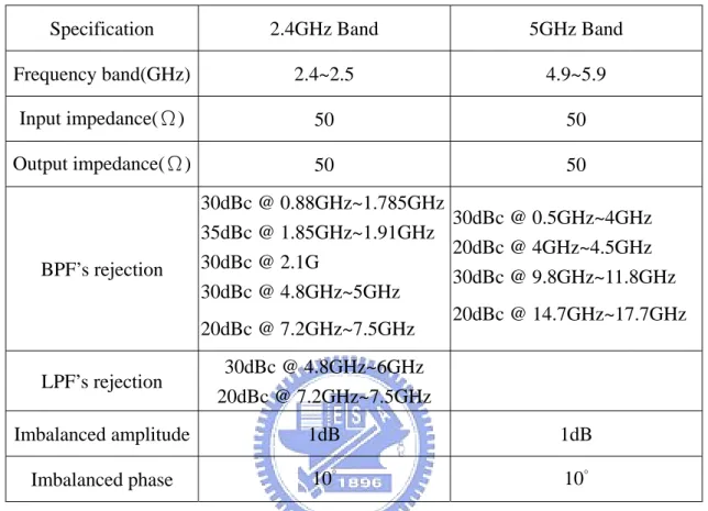
(11) 5470~5725 MHz for HIPERLAN/2. Currently the 2.4GHz band has been widely used for WLAN application. The market estimate shows a strong shift from 2.4 to 5GHz in the future. There have been numerous researches undertaken to integrate different applications, especially for applications in IEEE 802.11a/b and HIPERLAN/2 systems, in one piece of electronic equipment. Figure 1-1 shows the balanced diplexer module for WLAN. In this thesis this module will be implemented and integrated into LTCC technology to meet the specifications of IEEE 802.11a/b. For WLAN applications, the image signals need to be highly attenuated to maintain high quality signals received from the antenna. Moreover, the leakages of harmonics from the transmitted circuit to received circuit must be suppressed.. Rx:2.4 GHz. 2.4 & 5GHz. BPF diplexer BPF. 2.4 & 5GHz. Rx:5 GHz SW. 2.4/5 GHz. Part 1 Tx:2.4 GHz LPF. BPF. BLN. BPF. BPF. BLN. diplexer. Tx:5 GHz. Part 2. Part 3. Figure 1-1 LTCC balanced diplexer module for WLAN. For designing of baluns and low pass filters, the multi-layer structure of LTCC is quite useful. To achieve minimal dimension of the filter and broad stopband, this work is concentrated on stripline comblines filter. Using the technique of cross coupling to produce transmission zeros can increase the rejection at the lower stopband and reduce 2.
(12) the number of resonance. Therefore, the insertion loss, size, and the cost for manufacture and design are less at the same time.. Specification. 2.4GHz Band. 5GHz Band. Frequency band(GHz). 2.4~2.5. 4.9~5.9. Input impedance(Ω). 50. 50. Output impedance(Ω). 50. 50. BPF’s rejection. 30dBc @ 0.88GHz~1.785GHz 30dBc @ 0.5GHz~4GHz 35dBc @ 1.85GHz~1.91GHz 20dBc @ 4GHz~4.5GHz 30dBc @ 2.1G 30dBc @ 9.8GHz~11.8GHz 30dBc @ 4.8GHz~5GHz 20dBc @ 14.7GHz~17.7GHz 20dBc @ 7.2GHz~7.5GHz. LPF’s rejection. 30dBc @ 4.8GHz~6GHz 20dBc @ 7.2GHz~7.5GHz. Imbalanced amplitude. 1dB. 1dB. Imbalanced phase. 10°. 10°. Table 1-1 Specifications of the LTCC filters for WLAN. The dielectric constant of LTCC substrate is 33 and the conductor is silver with conductivity of 1.23 ×10⁸ S / m so that we can minimize the circuit as small as. possible. In Chapter2, the Marchand balun is implemented with two structures corresponding to two operating bands. We choose different structures for the two bands in order to get better response. In Chpater3, a simple-structure low pass filter is proposed because the high dielectric constant of the ceramic substrate. Moreover, we design the filter at higher cutoff frequency to reject second or third harmonics. In Chapter4, the three-pole combline filter with cross coupling is shown. Table 1-1 3.
(13) shows the specifications of the filter in Fig. 1-1. In Chapter5, we connect the bandpass filters and baluns as part3 in Fig.1-1 and use a lowpass filter of 2.4GHz and a bandpass filter of 5GHz to design the diplexers. Because of the high dielectric constant, the impedance matching becomes a big problem when designing the diplexers. We use lower system impedance (lower than 50Ω) to improve the diplexer performance. However, a broadband impedance transformer is needed to transform the system impedance to 50Ω.. 4.
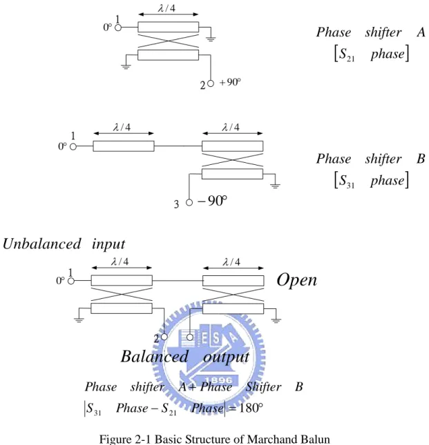
(14) Chapter 2 Balun The word, balun, is an acronym for a balanced-to-unbalanced transformer used to convert an unbalanced signal to two equal potential signals with 180-degrees phase difference. Generally a balun has three ports, but some four-port passive circuits, such as rat-race hybrids and waveguide magic-T, can also be used as baluns. Major limitations of these components are their narrow bandwidths and the lack of a method for grounding the center-tap. Marchand balun is a microwave balun and is important in realizing of balanced mixers, amplifiers, multipliers, and phase shifters. Through the use of multiple quarter-wave sections, it is theoretically possible to achieve a Chebyshev response up to one to six bandwidth [1]. As compared with a short-ended couple-line, this structure needs not to implement the coupler with high even-to-odd-mode impedance ratio. Generally the performance is good if Z Oe is 3 to 5 times of Z Oo in such structure. With proper parameters, the balun can even achieve a bandwidth of more than 10:1.. 2-1 Analysis of Marchand Balun Fig. 2-1 shows the basic structure and operation theory of the Marchand balun. This balun consists of two coupled-line sections, which can be realized by microstrip, Lange couplers, multilayer coupled structures, or spiral coupled-lines. The length of each section is about quarter-wavelength at the center frequency. The first section divides the signal into two signals with equal magnitude and phase over a broad frequency range and the second section provides –90 degrees and +90 degrees phase shift for these two signals that the two output signals will have 180 degrees phase difference.. 5.
(15) λ/4. 1. 0°. Phase shifter. [S21. + 90°. 2. 0°. λ/4. 1. phase]. A. λ/4. Phase shifter B [S31 phase] 3. − 90°. Unbalanced input 0°. λ/4. 1. λ/4. Open 2. Balanced output Phase shifter Phase − S 21. S 31. A + Phase Shifter. B. Phase = 180°. Figure 2-1 Basic Structure of Marchand Balun. Coupler1 Port 2 Port1. ZO. λ/4. Z1. Port 3 Coupler 2. Z1. Figure 2-2 Schematic of the symmetrical Marchand Balun. 6.
(16) The scattering matrix of a symmetrical balun can be derived from the scattering matrix of two identical couplers as Figure 2-2 shown. If the unbalanced input impedance is Z O and the balanced output impedance is Z 1 , the scattering matrix of an ideal coupler with the coupling factor C and infinite directivity, and the S-parameters of the balun are shown below [2].. [S ]ideal _ coupler. [ S ]balun. ⎡ 0 ⎢ C =⎢ ⎢− j 1 − C 2 ⎢ 0 ⎣⎢. − j 1− C2 0 0 C. C. 0 0 − j 1− C2. ⎡ ⎞ 2 ⎛ 2 Z1 + 1⎟ ⎢ 1− C ⎜ ⎝ ZO ⎠ ⎢ ⎢ ⎞ 2 ⎛ 2Z ⎢ 1 + C ⎜ 1 − 1⎟ ⎢ ⎝ ZO ⎠ ⎢ ⎢ 2C 1 − C 2 Z1 ⎢ ZO =⎢ j ⎞ ⎢ 2 ⎛ 2 Z1 ⎢ 1 + C ⎜ Z − 1⎟ ⎝ O ⎠ ⎢ ⎢ Z1 ⎢ 2C 1 − C 2 ZO ⎢ ⎢− j ⎢ 1 + C 2 ⎛⎜ 2Z1 − 1⎞⎟ ⎢⎣ ⎝ ZO ⎠. 2C 1 − C 2 j. Z1 ZO. ⎛ 2Z ⎞ 1 + C 2 ⎜ 1 − 1⎟ ⎝ ZO ⎠. 1− C2 ⎛ 2Z ⎞ 1 + C 2 ⎜ 1 − 1⎟ ⎝ ZO ⎠ ⎛ Z1 ⎞ 2C ⎜⎜ ⎟ Z O ⎟⎠ ⎝ j ⎛ 2Z ⎞ 1 + C 2 ⎜ 1 − 1⎟ ⎝ ZO ⎠. ⎤ 0 ⎥ − j 1− C2 ⎥ ⎥ C ⎥ 0 ⎦⎥. Z1 ⎤ ⎥ ZO ⎥ −j ⎛ 2Z ⎞⎥ 1 + C 2 ⎜ 1 − 1⎟ ⎥ ⎝ ZO ⎠⎥ ⎥ ⎛ Z1 ⎞ ⎥ 2C ⎜⎜ ⎟ Z O ⎠⎟ ⎥ ⎝ ⎥ j ⎞ ⎥ 2 ⎛ 2 Z1 1+ C ⎜ − 1⎟ ⎥ ⎝ ZO ⎠ ⎥ ⎥ ⎥ ⎥ 1− C2 ⎛ 2Z ⎞ ⎥ 1 + C 2 ⎜ 1 − 1⎟ ⎥ ⎝ ZO ⎠ ⎥⎦. 2C 1 − C 2. The scattering matrix of the balun above demonstrates by using two identical coupled sections results in the outputs with equal amplitude and opposite phase, regardless of the coupling factor and port terminations. In order to achieve optimum equal power transfer(-3dB), we require that: S 21 = S 31 = 2C 1 − C 2 ⇒. Z1 ZO. ⎛ 2Z ⎞ 1 + C 2 ⎜⎜ 1 − 1⎟⎟ ⎝ ZO ⎠. 1 2 2. =. ⎡ ⎛ 2Z ⎞ ⎤ ⇒ ⎢C 2 ⎜⎜ 1 + 1⎟⎟ − 1⎥ = 0 2 ⎠ ⎦ ⎣ ⎝ ZO. 1. 7.
(17) 1. ∴ C=. 2Z 1 +1 ZO. When the source impedance Z O and the load impedance Z 1 are given, we can get the coupling factor and design Marchand balun. For example, if all ports are terminated with 50Ω, the required coupling factor is –4.8dB.. 2-2 Realization of the Marchand Balun for LTCC There are two steps to construct the Marchand balun in LTCC structure: the multi-layer structure and meander and/or spiral lines.. The coupled-line width is. limited by the circuit size and the processes. We can obtain proper coupling by controlling the layer thickness. In fig. 1-1, one balun is designed to operate in the frequency range of 2.4~2.5GHz, and the other is in the frequency range of 4.9~5.9GHz. Unbalanced input impedance and two balanced output impedances are all 50Ω. Each design we have proposed two structures. One is to put these two sections in the same plane as shown in Fig. 2-3(a), and the other is to stack them up as shown in Fig. 2-3(b).. (b ) Structure2. ( a ) Structure1. Figure 2-3 Two structures of LTCC Marchand Balun 8.
(18) 2_4GHz Balun. 0 -5 -10 -15 -20 -25 -30. DB(|S(1,1)|) Balun1. DB(|S(1,1)|) Balun2. DB(|S(2,1)|) Balun1. DB(|S(2,1)|) Balun2. DB(|S(3,1)|) Balun1. DB(|S(3,1)|) Balun2. 2.4 GHz 2.5 GHz. 1.5. 2. 2.5 Frequency (GHz). 3. 3.5. Figure 2-4 The performance of 2.4~2.5GHz Balun. For 2.4~2.5GHz balun, the overall size of structrue1 is 160mil×50mil×22.2mil and that of structure2 is 80mil×50mil×42mil. For 4.9~5.9GHz balun, the overall size of structrue1 is 100mil×50mil×22.2mil and that of structure2 is 70mil×50mil×42mil.. Balun1 (L) Magnitude Difference. Balun2 (L) Magnitude Difference. Balun1 (R) Phase Difference. Balun2 (R) Phase Difference. Imbalance. 2. 3. 1. 2.25. 0. 1.5. -1. 0.75. -2. 2.4 GHz. 2. 2.2. 0. 2.5 GHz. 2.4 2.6 Frequency (GHz). 2.8. 3. Figure 2-5 The imbalance of 2.4~2.5GHz Balun. The simulated results are shown in Fig. 2-4, Fig. 2-5, Fig. 2-6, and Fig. 2-7 9.
(19) respectively. In the operating frequency band, the insertion loss and the return loss are less than –0.3dB and –18dB for 2.4~2.5GHz balun while the insertion loss and the return loss are less than –0.8dB and –10dB 4.9~5.9GHz balun respectively. The amplitude and phase imbalances of structure2 for 2.4~2.4GHz between balanced outputs are within 0.5dB and 0.6°, while the imbalances of structure1 for 4.9~5.9GHz between balanced outputs are within ±0.5dB and 4.5° respectively.. 5GHz Balun. 0. -10. -20. -30. DB(|S(1,1)|) Balun1. DB(|S(1,1)|) Balun2. DB(|S(2,1)|) Balun1. DB(|S(2,1)|) Balun2. DB(|S(3,1)|) Balun1. DB(|S(3,1)|) Balun2. -40. 4. 9 GHz. 3. 4. 5.9 GHz. 5 Frequency (GHz). 6. 7. Figure 2-6 The performance of 4.9~5.9GHz Balun Balun2 (L) Magnitude Difference. Balun1 (L) Magnitude Difference. Balun2 (R) Phase Difference. Balun1 (R) Phase Difference. Imbalance. 2. 9. 1. 6.75. 0. 4.5. -1. 2.25. -2. 4.902 GHz. 4. 4.5. 0. 5.9 GHz. 5 5.5 Frequency (GHz). 6. 6.5. Figure 2-7 The imbalance of 4.9~5.9GHz Balun. 10.
(20) Apparently, the imbalances of 4.9~5.9GHz balun are worse than that of 2.4~2.5GHz one. The challenge is that the former needs about 19% of fractional bandwidth. No doubt the structure2 is smaller, and the performance and imbalance are better than structure1 for 2.4~2.5GHz, so we choose structure2 to connect it with a bandpass filter as part3 in Fig.1-1. For 4.9~5.9GHz application, under the consideration for the module arrangement and the response, structure1 is chosen. The overall simulated results are shown in Chapter5.. 11.
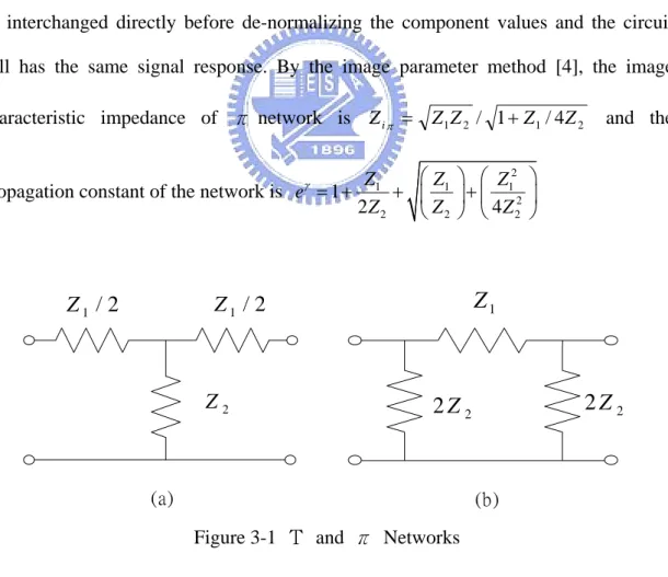
(21) Chapter 3 Low Pass Filter In this chapter, constant-k and m-derived filter lowpass filters are presented and then implement the low pass filters using low temperature co-fired ceramic.. 3-1 Analysis of m-derived filter Two important building blocks, namely Τ and π circuits, are commonly used to construct the lowpass ladder network, which can be made in the symmetric form. The element values of a filter prototype were taken from the Butterworth table [3] and can be arranged as π or Τ network. The arrangements of capacitors and inductors can be interchanged directly before de-normalizing the component values and the circuit still has the same signal response. By the image parameter method [4], the image characteristic impedance of π network is Z i π = Z 1 Z 2 / 1 + Z 1 / 4 Z 2. and the. ⎛ Z1 ⎞ ⎛ Z12 ⎞ Z1 propagation constant of the network is e = 1 + + ⎜ ⎟+⎜ 2 ⎟ 2Z 2 ⎝ Z 2 ⎠ ⎝ 4Z 2 ⎠ γ. Z1. Z1 / 2. Z1 / 2. Z2. 2Z 2. 2Z 2. (a). (b). Figure 3-1 Τ and π Networks. A constant-k section is a symmetrical two-port network and, therefore, the input impedance (or image impedance) is equal to the output image impedance of the filter 12.
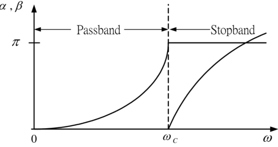
(22) section. Consider a π network shown in Fig. 3-1(b), a low pass filter can be formed by combining a series inductor and two shunt capacitors which tend to block high-frequency signals while passing low-frequency signals. That we can get Z 1 = jwL and. Z 2 = 1 / jwC . So the constant-k section has an image impedance that. is a function of frequency and is defined as: Z iπ = RO / 1 −. ω2 , ω c2. where ωc =. ωc : the cutoff. L/2. frequency;. eγ = 1 −. 2 LC. 2ω 2. ωc 2. and. +. 2ω. ωc. RO =. ω2 −1 ωc 2 L =k C. RO : nominal characteristic impedance. L/2. L. C/2. C. C/2. Figure 3-2 Low pass constant-k filter section inΤ and π form. α,β Passband. π. Stopband. ωC. 0. ω. Figure 3-3 Typical passband and stopband characteristics of the lowpass constant-k sections. For ω < ωc (passband): Z iπ is real and γ is imaginary. 13.
(23) 2. e. γ 2. ⎛ 2ω 2 ⎞ 4ω 2 ⎛ ω 2 ⎞ = ⎜1 − 2 ⎟ + 2 ⎜1 − 2 ⎟ = 1 ⎝ ωc ⎠ ωc ⎝ ωc ⎠. For ω > ωc (stopband): Z iπ is imaginary and γ is real. When ω. ωc the. attenuation rate is 40dB/decade. The dependency on frequency is a limitation of the filter section since the image impedance will not match constant source or load impedance. This disadvantage, as well as the fact that the attenuation is rather small near cutoff, can be remedied with the modified m-derived sections.. (1 − m ) C 2. mL / 2. mL / 2. 4m. mC. mL. (1 − m ) L 2. mC / 2. mC / 2. 4m. Figure 3-4 m-derived filter section. The m-derived section is a modification of the constant-k section and both sections still maintain the same image impedances as defined in [4]. But the new m-derived Τ section has an LC series resonance in the shunt arm of the filter and the new m-derived π section has an LC shunt resonance in the series arm to provide an additional freedom as shown in Fig. 3-4. This resonance provides the ability to modify the passband attenuation. The resonant frequency of the LC arm is defined as. ω∞ =. ωc 1 − m2. , 0 < m < 1 (note: if m is set to one, the passband characteristics are. identical to those of the constant-k section.) Although the m-derived section can get a very sharp cutoff response, the nonconstant image impedance still exists because of the dependence on m; moreover, its attenuation decreases for ω > ω∞ . Since it is 14.
(24) often desirable to have infinite attenuation as ω → ∞ , the m-derived section can be cascaded with a constant-k section to give the composite attenuation response. From Fig. 3-5 we see that by combining in cascade the m-derived section and the constant-k section can keep the sharp cutoff and the constant-k section provides high attenuation further in to the stopband. This type of design is called a composite filter.. α Composite response. m − derived attenuation. Constant − k. 0. attenuation. ω. ωC ω∞. Figure 3-5 Typical attenuation responses. (1− m ) C 2. L. 4m. mL 1+ m C mC / 2 2. C/2. Figure 3-6 The composite filter. 3-2 Design and realize LTCC low pass filter From the analysis described above, we can realize the filter with the desired attenuation by using the composite filter. Because the filter should pass 2.4GHz signal, 15.
(25) the first design is a filter with cutoff frequency at 3.3GHz, the impedance of 50Ω, and the finite frequency attenuation pole at 5GHz.. L=. 2 Ro. ≅ 4.823 ×10⁻⁹ H = 4.823nH. 2. ≅ 1.93 × 10⁻¹² C = 1.93 pF. ωc. C=. Roωc. 2. 2. ⎛ f ⎞ ⎛ 3.3 ×10⁹ ⎞ ≅ 0.75 m = 1− ⎜ c ⎟ = 1− ⎜ 9 ⎟ ⎝ 5 × 10 ⎠ ⎝ f∞ ⎠. Τ type. m L 2. 1.8 nH. C2 = mC. 1.45pF. L1 =. L2 =. 1 − m2 L 4m. 0.7 nH. L3 =. 1+ m L 2. 4.22nH. π type. m C 2. 0.725pF. L1 = mL. 3.62 nH. C1 =. 1 − m2 C 4m. 0.28 pF. 1+ m C C1 2. 1.70 pF. C2 = C3 =. C4 = C. 1.93nH. L4 = L. 4.823nH. L 2. 2.4nH. C5 =. C 2. 0.965pF. L5 =. Table 3-1 The corresponding component values of low pass filter forΤ and π types IND ID=L2 L=3.62 nH IND ID=L4 L=4.823 nH. PORT P=1 Z=50 Ohm. CAP ID=C1 C=0.725 pF. CAP ID=C2 C=0.28 pF. CAP ID=C3 C=1.7 pF. PORT P=2 Z=50 Ohm. CAP ID=C5 C=0.965 pF. :. 16.
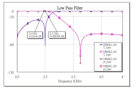
(26) Low Pass Filter. 0 -10. 2.5 GHz -0.000308 dB. 2.4 GHz -0.01646 dB. -60. DB(|S(1,1)|) T_type DB(|S(2,1)|) T_type DB(|S(2,1)|) pi_type DB(|S(1,1)|) pi_type. -110 0.5. 2.5. 4.5 Frequency (GHz). 6.5. 8. Figure 3-7 Circuit Simulation of the low pass filter by Microwave Office The simulation results by using MicrowaveOffice are shown in Fig. 3-7. Here we choose π type section for the process consideration. Next, try to convert the ideal inductance and capacitance into LTCC structure. Because we have calculated the component values of low pass filter, by the exported spice-model file the lengths and widths of the transmission line with corresponding capacitances and inductance can be estimated. Fig. 3-8 shows the configuration of proposed stripline LPF. This filter is a kind of semi-lumped LPF using two sections of m-derived units. Because the high dielectric constant of LTCC material is used, we can only control the dielectric thicknesses to get the needed capacitances instead of large size parallel-plate capacitor.. Figure 3-8 The configuration of proposed stripline LPF 17.
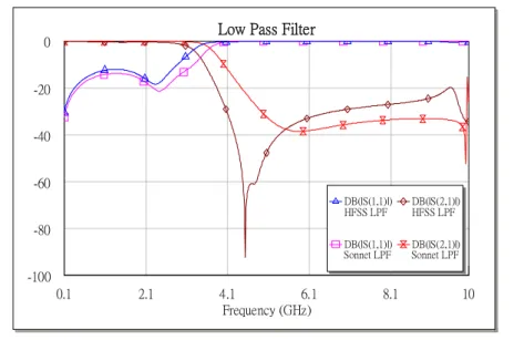
(27) Low Pass Filter. 0 -20 -40 -60. DB(|S(1,1)|) HFSS LPF. DB(|S(2,1)|) HFSS LPF. DB(|S(1,1)|) Sonnet LPF. DB(|S(2,1)|) Sonnet LPF. -80 -100 0.1. 2.1. 4.1 6.1 Frequency (GHz). 8.1. 10. Figure 3-9 EM simulation of lowpass filter by Sonnet and HFSS. 18.
(28) Chapter 4 Band Pass Filter. 1. 2. n1. 3. n. Output. Input. Figure 4-1 Typical combline bandpass filter. 4-1 Theory of the typical combline filter As shown in Fig. 4-1, a typical tapped combline filter consists of mutually coupled resonators. The lines are each short circuited to ground at the same end while opposite end are terminated in lumped capacitors that the physical length can be reduced less than a quarter wavelength by loading capacitive loads. As the capacitors are increased the shunt lines behave as inductive elements and resonate with the capacitors at a frequency below the quarter-wave frequency. The larger the loading capacitances, the shorter the resonator lines, which results in a more compact filter structure with a wide stopband between the first passband and the second passband. If the capacitors are not present, the resonator line will be λ0 / 4 long at resonance, and the structure will have no passband because the magnetic and electric couplings cancel each other out in this case. For a typical filter using λO / 4 resonators, the second passband occurs approximately at three times of main passband frequency. If the resonator lines are 19.
(29) λO / 8 at the center frequency, the second passband will be pushed at about four times of the first passband frequency. So when the resonator lines are less than λO / 8 at the primary passband, the second passband can be even pushed to higher frequency.. a. YOe , YOo. b. YOe , YOo. a. a. b. YOo a − YOe a = vCab 2. b. θ. θ. 1. 2. θ YOe b = vCb. YOe a = vCa. Figure 4-2 Transformation of the equivalent circuit of a coupled line. θ. 1. J = Yo cot θ ,. YO. 2. θ. θ ≠ 90°. J. 1. −YO. −YO. Figure 4-3 The schematic diagram of J-inverter Y = vCab. Cas. Y = vCbc. θ Cbs. Ccs. θ. Y = vCa. Y = vCb. Y = vCc. Figure 4-4 The equivalent circuit of the combline filter. 20. 2.
(30) According to the Grayzel and Matthaei’s methods [8,9], the equivalent circuit of a combline filter as shown in Fig. 4-4 is derived form the coupled lines of Fig. 4-2. While. θ ≠ 90° the combline filter can be equivalent to a J-inverter connected with two shunt arms under the condition, J = YO cot θ , that we can get the J-inverter equivalent circuit of a combline filter in Fig. 4-5.. Cas. J12. Cbs. J 23. Yai = v(Ci + Ci −1,i + Ci ,i +1 ). θ. Ya1. Ccs. Ya 3. Ya 2. Figure 4-5 The J-inverter equivalent circuit for the combline filter. Next, denote Φ 21 the phase of Y-parameter S21. First consider the series capacitor as two port devices in Fig. 4-6(a). The signal from port1 will undergo a phase shift after going through the capacitor. The phase shift, Φ 21 , tends toward +90°. When the capacitor is replaced by a inductor, the phase shift will become -90°. In Fig. 4-6(c) shows the phase shift of a shunt inductor/capacitor pairs. The inductance and capacitance can determine a resonance frequency. Below the resonance frequency, the phase shift tends toward +90° while above the resonance frequency the phase shift tends toward -90°. Shown in Fig. 4-7(a) is a coupling structure of cascaded trisection or CT filter. Path 1-2-3 is the primary path and path 1-3 is the secondary path which follows the capacitive cross-coupling. Below the resonance frequency the phase of path 1-2-3 is 270° while the phase of path 1-3 is 90°, this means these two paths are out phase. 21.
(31) Above the resonance frequency these paths are in phase. This destructive interface causes a transmission zero on the low-side skirt as shown in Fig. 4-7(b). If the coupling between 1 and 3 is stronger the zero will move toward the passband, and vice versa.. Y =−j. Y = jωC. Port 1. Port 2. 1 ωL Port 2. Port 1 Φ 21 = −90°. Φ 21 = +90°. (b ). (a) Φ 21 = ang (Y21 ) +90°. Port 1. Port 2 −90°. (c). Resonant. frequency. Figure 4-6 Phase shifts for (a) Series capacitor (b) Series shunt (c) Shunt inductor/capacitor pairs 2. K12 Qe1. 1. K23. K13. 3. Qe2. (a). (b). Figure 4-7(a) The coupling schematic of three-pole cross-coupled filter Figure 4-7(b) Possible transmission response of CT type bandpass filters. 22.
(32) Below Resonance frequency. Above Resonance frequency. Path 1-2-3. 90°+90°+90°=270°. -90°-90°-90°= -270°=90°. Path 1-3. 90°. 90°. Phase shift. Out phase. In phase. Table 4-1 Phase shifts for two paths in a CT section with capacitive cross-coupling. 4-2 Design of the LTCC combline filter with cross-coupled capacitor As discussed in chapter 4-1 we can use CT structure with the capacitive crosscoupling between the resonators 1 and 3 to generate a zero in the low-side skirt. The proposed structures are shown in. 4-8. It is confirmed that the combline filter with cross coupling capacitor has two wave propagation paths. One is the cross-coupled capacitor and the other is the coupling through the adjacent resonators. Fig. 4-8(b) is a modification of Fig. 4-8(a). The coupling between adjacent resonators can be easily tuned with the direct-coupled capacitors. Moreover, the edge coupling restricts the bandwidth of the typical combline filter that the modified combline filter with direct-coupled capacitors can achieve larger bandwidth. Cross − coupling Capacitors. C13. C13. C10 C20. C10. C30. C20. I / O Port I / O Port. I / O Port. C30 I / O Port. Coupled Capacitors. (a). (b ). Figure 4-8 Equivalent circuits of three-pole combline filter with (a) coupled-line (b) coupled capacitors 23.
(33) Magnitude and Phase of Admittance. 50. 100. 0. 60. -50. 20 DB(|Y(2,1)|) (L) Schematic 1 DB(|Y(2,1)|) (L) Schematic 2. -100 4.33 GHz -45.39 dB. -20. Ang(Y(2,1)) (R, Deg) Schematic 1. -150. -60. Ang(Y(2,1)) (R, Deg) Schematic 2. -200. -100 0.1. 5.1. 10.1. 15. Frequency (GHz). Figure 4-9 Phase and magnitude of two paths’ admittance. When the loading capacitances and the length of the resonator lines are given, the resonance frequency is determined. Fig. 4-9 shows the magnitude and phase of admittance, Y21. As mentioned in Section 4-1, because path 1-3 and path 1-2-3 are out-off phase below the resonance frequency, the transmission zero occurs at the frequency where these two paths have the same magnitude but opposite phase. The design steps are as follows: 1.. Choose the optimum loading capacitors. The adaptive capacitance not only shortens the resonance lines to reduce the total circuit size but also results in a wider stopband between the first and the second passband. The value of the MIM capacitors is not very large under the restriction of the circuit size.. 2.. Using transmission lines as resonances to get wanted resonance frequency.. 3.. Choose C12 and C23 that can control the bandwidth of the filter, and C13, which can determine the position of the transmission zero.. 4.. Fine tune.. Initial design are simulated by Microwave Office and then implemented in LTCC 24.
(34) structure by EM-simulation tools, Sonnet and HFSS. CA P ID = C 13 C = 0.3 2 pF. C AP ID = C 1 0 C = 4 .2 4 p F PO R T P=1 Z= 50 O h m S SUB E r = 33 B = 1 6.2 m il T = 1 .4 m il R ho = 1 T a nd = 0 N am e = S S U B 1. CAP ID = C 2 0 C = 3 .93 p F C AP ID = C 1 2 C =1 pF. S L IN ID = S L1 W = 5 .2 m il L = 8 1 m il. S L IN ID = S L 2 W = 5 .2 m il L= 8 1 m il. CAP ID = C 3 0 C A P C = 4 .24 p F ID = C 2 3 C =1 pF. S L IN ID = S L 3 W = 5 .2 m il L = 8 1 m il. PO RT P= 2 Z =50 O hm. 2_4GHz BPF. 0 -10 -20 -30 -40 -50 -60 -70 -80 -90 -100 -110 -120. 4.8 GHz -30.12 dB. 6 GHz -34.54 dB. 7.2 GHz 7.5 GHz -37.56 dB -38.2 dB 2.4 GHz -32.93 dB. 2.5 GHz -30.81 dB. DB(|S(1,1)|) Schematic 1 DB(|S(2,1)|) Schematic 1. 0.1. 5.1. 10.1. 14. Frequency (GHz). Figure 4-10 Circuit simulation results of 2.4~2.5GHz Bandpass filter. GND. ( a ) 2.4 ~ 2.5G H z. (b ) 4.9 ~ 5.9GHz. Figure 4-11 3D structure of LTCC combline filter 25.
(35) The component values of the 2.4~2.5GHz bandpass filter is shown in Fig. 4-10. This filter can suppress not only the second and the third harmonic frequency signals but also the lower side stopband signals. Next, we convert these values into LTCC structure. The circuit size is 100 mil×75 mil×31.2mil. As shown in Fig. 4-12, there is an extra transmission zero in the lower-side skirt. The vias which connect the resonance line to ground can be equivalent to an inductor. From Microwave Office simulation we can estimate the inductance is about 0.028nH and the spice model file exported from Sonnet also shows the equivalent inductance is about 0.028nH at low frequency. 2.4 GHz -0.02718 dB. 0 -10 -20 -30 -40 -50 -60 -70 -80 -90 -100 -110 -120. 2.5 GHz -0.03528 dB. Sonnet 2_4GHz BPF 7.2 GHz -41.57 dB. 2.1 GHz -40.08 dB. 4.8 GHz -31.39 dB. 7.5 GHz -43.59 dB. 5 GHz -32.32 dB. 2.4 GHz 2.5 GHz -22.04 dB -20.93 dB DB(|S(1,1)|) bpf12 DB(|S(2,1)|) bpf12. 0.5. 1.5. 2.5. 3.5. 4.5 5.5 6.5 Frequency (GHz). 7.5. 8.5. 9.5 10. Figure 4-12 EM simulation results of 2.4~2.5GHz Bandpass filter Magnitude and Phase of Admittance with an inductor. 200. 100 CAP ID=C13 C=0.319 pF. PORT P=3 Z=50 Ohm. PORT P=4 Z=50 Ohm. 0 CAP ID=C20 C=3.93 pF. CAP ID=C10 C=4.18 pF PORT P=1 Z=50 Ohm. CAP ID=C23 C=0.9 pF. CAP ID=C12 C=0.9 pF. SLIN ID=SL2 W=6 mil L=73 mil. SLIN ID=SL1 W=6 mil L=73 mil. CAP ID=C30 C=4.18 pF PORT P=2 Z=50 Ohm. -100. SLIN ID=SL3 W=6 mil L=73 mil. Ang(Y(2,1)) (Deg) Schematic 1. DB(|Y(4,3)|) Schematic 1. Ang(Y(4,3)) (Deg) Schematic 1. DB(|Y(2,1)|) Schematic 1. -200 0.1 SSUB Er=33 B=16.2 mil T=1.4 mil Rho=1 Tand=0 Name=SSUB1. 5.1. IND ID=L1 L=0.0028 nH. 10.1 Frequency (GHz). 15.1. 20. Figure 4-13 Phase and magnitude of two paths’ admittance with an inductor 26.
(36) Fig. 4-15 is the comparison between measured result by GSG probe and simulated result. The insertion loss in the passband (2.4~2.5GHz) is about 2.5dB. The return loss is less than –10dB from 2.35 to 2.55GHz. The suppression for second and third harmonic is below –30dB.. Figure 4-14 Photograph of the LTCC Combline Filter. DB(|S(1,1)|) Measurement. DB(|S(2,1)|) Measurement. DB(|S(1,1)|) Simulation. Graph 1. DB(|S(2,1)|) Simulation. 0. -20. -40. -60 2.0213 GHz -30 dB. -80. -100 0.045. 2.04. 4.05 6.05 Frequency (GHz). 8.04. 10. Figure 4-15 Comparison of measured (GSG Probe) and simulated results 27.
(37) Because the measured result is a little different from the simulated result, we slice the circuit to check the layout again to make sure of the factors which may affect the consistency.. 剖面觀察區 ( Line 1 ):定義為背面. 剖面觀察區 ( Line 2 ) :定義為正面. Figure 4-16 Cross-sectional views of 2.4~2.5GHz LTCC combline filter. It is clear that the G and E layers don’t overlap as shown in Fig. 4-16. However, in 28.
(38) our original design, the overlaps between these two layers control the coupling of adjacent resonators. Decreasing of this overlapping will directly affect the bandwidth of the combline filter. This is why the bandwidth in measured result is smaller than the simulated result. Next, use the same method to design 4.9~5.9GHz bandpass filter. This filter’s size is 90 mil×50 mil×32.4mil. Fig. 4-17 shows EM simulations of Sonnet and HFSS. For Sonnet the Box consists of perfect E while for HFSS the Box and metals with dielectric loss tangent, 0.001, and bulk conductivity, 1.23×10⁸ are used, so we care about HFSS simulated results more than Sonnet simulated results.. DB(|S(1,1)|) HFSS 5GBPF_setup1. DB(|S(1,1)|) HFSS 5GBPF_setup2. DB(|S(1,1)|) HFSS 5GBPF_setup3. DB(|S(1,1)|) Sonnet 5GHz BPF. DB(|S(2,1)|) HFSS 5GBPF_setup1. DB(|S(2,1)|) HFSS 5GBPF_setup2. DB(|S(2,1)|) HFSS 5GBPF_setup3. DB(|S(2,1)|) Sonnet 5GHz BPF. 5GHz BPF. 0 -10 -20 -30 -40 -50 -60 -70. 4.902 GHz5.901 GHz. 0.5 1.5 2.5 3.5 4.5 5.5 6.5 7.5 8.5 9.5 10.511.512.513.514.515.516.517.518.519.520 Frequency (GHz). Figure 4-17 EM simulation results of 4.9~5.9GHz Bandpass filter. 29.
(39) Chapter 5. 5-1 Diplexer Nowadays, diplexers are essential components in modern RF front module to separate a multiband or transmit/receive frequencies. In some instances they isolate transmitting and receiving channels, and in other cases separate bands at different frequencies for different receiver channels. In this thesis we use two diplexers to separate different-frequency bands for Tx and Rx, respectively. The basic components of the diplexer are a lowpass filter, a bandpass filter, and a matching network between them. An ideal diplexer is designed that for 2.4GHz band the other output port is open for 2.4~2.5GHz signal, i.e. it seems that the other output port doesn’t exist. Similarly, for 4.9~5.9GHz signal the 2.4GHz end is open.. 2. 2.4GHz BPF Z1 ,θ1. 1. 50Ω. 50Ω. 3. 5GHz BPF Z 2 ,θ 2. 50Ω. Figure 5-1 The Configuration of the LPF/BPF diplexer In order to simplify the design process and save the simulation time, we separate the diplexer into two parts. First, because the other part is required as an open end for one part, for 2.4~2.5GHz low pass filter change the impedance and electrical length of the transmission line to set S11 at 4.9~5.9GHz near the open point on the Smith Chart. 30.
(40) S(1,1) Part2_24G Swp Max. 1.0. 0.8. 2 .0. 2 .0. 0.6. 10GHz. 0.6. 10GHz. 4.9 GHz r 0.00614771 x 1.90037. S(1,1) Part2_24G Swp Max. Part2_24G_2. 4.9 GHz r 0.0104407 x 2.71723. 0.4. 0.8. 1.0. Part2_24G_2. 0.4. 3. 0. 4.0. 3. 0. 4.0. 5.0. 5.0 0.2. 10.0. 4.0 5.0. 3.0. 2.0. 5.4 GHz r -0.00418608 x -13.9078. 1.0. 0.8. 0.6. 0.4. 0.2. 0. 10.0. 4.0 5.0. 3.0. 2.0. 1.0. 0.8. 0.6. 0.4. 0. 10 .0. -1 0.0 0. .0. -0 .6. Swp Min 0.1GHz. -1.0. -0 .8. -1.0. -0 .8. -0 .6. -2.. Z 0 = 40Ω. 0. -3. Swp Min 0.1GHz. EL = 57.5 @ 2.45GHz. ;. 5.9 GHz r -0.000988577 x -2.06132. 4. -2.. -4 .0 . -0. .0. 5.9 GHz r -0.00127628 x -2.15704. 4. Z 0 = 35Ω. 2.45 GHz r 0.858417 x -0.222674 -3. -5.0. . -0. -0.2. -4 .0. 2.45 GHz r 0.682146 x -0.263992. -5.0. -0.2. -1 0.0. 0.2. 0.2 10 .0. 5.4 GHz r -0.429804 x 129.125. EL = 57.5 @ 2.45GHz. ;. Figure 5-2 The Smith Chart of 2.4GHz part S(1,1) Part2_5G. 0.8. 1.0. Swp Max 10GHz. 2. 0. 2. 0. 0.6. 1.0. 10.0. 3.0. -4.0 -3. 4. .0. Z 0 = 35Ω. ;. EL = 158@ 2.45GHz. Z 0 = 40Ω. ;. -1.0. -0 .6. Swp Min 0.1GHz. -0 .8. -1.0. -0 .8. -0 .6. -2.. 0 -2.. 0. . -0. .0. 4. -3. . -0. 10 .0. 2.5 GHz r 45.9856 x -4497.91. 5.9 GHz r 1.1656 x -0.307265. -0.2. 2.0. 1.0. 0.8. 0.6. 0.4. 0.2. 5.4 GHz r 0.739498 x -0.0112199. 0. 10.0. 4.0 5.0. 3.0. 2.0. 0.8. 0.6. 1.0. 2.5 GHz r 0.000916575 x -17.7828. -5.0. 0.4. 5.0. 2.4 GHz r 0.000341537 x 12.2145. -4.0. -0.2. 4.0. 10 .0. -1 0.0. 0.2. 5.9 GHz r 1.17564 x -0.264002. 2.4 GHz r 0.00183018 x 25.0718. 3 .0. 4.9 GHz r 0.727576 x 0.0812203. 5.0 0.2. 0.2. 4.0. -5.0. 0.4. 5.4 GHz r 0.71025 x 0.0552176. 0. 0.4. 3 .0. 4.9 GHz r 0.647997 x 0.156739. 4.0 5.0. 0.8. 0.6. S(1,1) Part2_5G. Part2_5G_2. Swp Max 10GHz. -1 0.0. Part2_5G_2. Swp Min 0.1GHz. EL = 158 @ 2.45GHz. Figure 5-3 The Smith Chart of 5GHz part When the impedance of the transmission line rises, the curve near passband of the filter will move toward the center of Smith Chart that the impedance matching is better. At the same time, we can observe the curve of S11 in the left figure at the frequencies where the other end desired as open spread wider than that in the right figure.. 31.
(41) Part2_24G_1. 10. Part2_24G_1. 10. 0. 0 DB(|S(1,1)|) Part2_24G. -10. DB(|S(1,1)|) Part2_24G. -10. DB(|S(2,1)|) Part2_24G DB(|S(1,1)|) 24GLPF. -20. DB(|S(2,1)|) Part2_24G DB(|S(1,1)|) 24GLPF. -20. DB(|S(2,1)|) 24GLPF. -30. DB(|S(2,1)|) 24GLPF. -30. -40. -40 0.1. 2.1. 4.1 6.1 Frequency (GHz). (a ) Z. 0. 8.1. 10. 0.1. = 35Ω. 2.1. 4.1 6.1 Frequency (GHz). 8.1. 10. (b) Z 0 = 40Ω Part2_5G_1. 20 0 -20 -40 -60 -80. DB(|S(1,1)|) Part2_5G. DB(|S(1,1)|) 5GBPF. DB(|S(2,1)|) Part2_5G. DB(|S(2,1)|) 5GBPF. -100 0.1. 2.1. 4.1 6.1 Frequency (GHz). 8.1. 10. Figure 5-4 The performance of the filter with the matching network Under the limitations of the design rule and the material, the maximum impedance is only about 32Ω for the stripline. So we try to lower the system input impedance that an extra transformer is needed. Next, we still want to save time to simulate and design so first make sure if EM simulation consists with the circuit simulation of combining three S-parameter files, where the three files are get from EM simulation separately, or not. The Comparison between EM and Circuit simulated results is shown in Fig. 5-5. Apparently, besides a little shift for the lowpass filter, the overall curves are almost the same. It indicates that the matching network can be separately designed, and connecting these three S-parameter files can get accurate responses of the diplexer. 32.
(42) Comparison between EM and Circuit simulated results. 0. -20. -40. 2.59 GHz -50.16 dB. -60. 2.68 GHz -44.08 dB. -80 0.1. 2.1. DB(|S(1,1)|) Circuit Simulation. DB(|S(1,1)|) EM Simulation. DB(|S(2,1)|) Circuit Simulation. DB(|S(2,1)|) EM Simulation. DB(|S(3,1)|) Circuit Simulation. DB(|S(3,1)|) EM Simulation. 4.1 Frequency (GHz). 6.1. 7. Figure 5-5 The Comparison between EM (Sonnet) and Circuit (MWO) simulated results. Ideal Transmission line. 0 -10 -20 -30 -40 -50 -60 -70. DB(|S(1,1)|) Schematic 2. DB(|S(2,1)|) Schematic 2. DB(|S(3,1)|) Schematic 2. -80 0.1. 2.1. 4.1 Frequency (GHz). 6.1. 7. Figure 5-6 The diplexer using ideal transmission lines After designing a 2.4GHz lowpass filter and a 5GHz bandpass filter in a 130 mil× 110 mil× 37 mil box, import the S-parameter files into Microwave Office and use the ideal transmission line to design in the first step. The simulated result is in Fig. 5-6 where the input impedance is 20Ω. The line in LTCC structure is different with the ideal transmission line, so we can only try to fit these two curves as close as possible. Fig. 5-7 shows EM simulations by HFSS and Sonnet.. 33.
(43) Figure 5-7 EM simulations of a LPF/BPF diplexer by HFSS. Figure 5-8 EM simulations of a LPF/BPF diplexer with a lowpass filter by HFSS 34.
(44) Because the system input impedance is reduced to 20Ω, an impedance transformer is needed which covers a wide range of frequencies from 2GHz to 6GHz. Here we use constant-Q match to design the transformer. The circuit in Fig. 5-9 is known as a constant-Q match because of its shape, and it does have the attribution of simplicity. For the application over 2GHz to 6GHz, a two-order transformer is used. First, select the impedance between 2GHz to 6GHz and calculate the values of Q, L and C by using the equations in Fig.5-9. Because the first deep of constant-Q match is at f 0 , when calculating these values, we choose f 0 as 2.45GHz that for 2.4~2.5GHz band the impedance matching is good. Next fine-tune the component values to make the second deep around or in 4.9~5.9GHz band.. L R1 −1 = R2. Q= C. R2. R1. Bp Xs = R2 1/ R1. ∴ X s = Qi R2 , B p = Figure 5-9 Constant-Q match (L-match). Part2. 0 -10 -20 -30 -40 -50 -60 -70 DB(|S(1,1)|) Part_LPF. -80. DB(|S(2,1)|) Part_LPF 2.3999 2.5022 GHz GHz. 0.1. 2.1. DB(|S(3,1)|) Part_LPF 4.8941 GHz. DB(|S(1,1)|) Part2. DB(|S(2,1)|) Part2. DB(|S(3,1)|) Part2. 5.9086 GHz. 4.1 6.1 Frequency (GHz). 8.1. 10. Figure 5-10 The performance of the LPF/BPF diplexer from 0.1~10GHz. 35. Q R1.
(45) Part2_2rd Harmonic. 0 -10. DB(|S(1,1)|) Part_LPF. DB(|S(2,1)|) Part_LPF. DB(|S(3,1)|) Part_LPF. DB(|S(1,1)|) Part2. DB(|S(2,1)|) Part2. DB(|S(3,1)|) Part2. -20 -30 -40 -50 -60 -70 -80 10. 10.5. 11 Frequency (GHz). 11.5. 12. Figure 5-11 The second harmonic of the LPF/BPF diplexer. Part2_3rd Harmonic. 0 -10. DB(|S(1,1)|) Part_LPF. -20. DB(|S(2,1)|) Part_LPF. DB(|S(3,1)|) Part_LPF. DB(|S(1,1)|) Part2. DB(|S(2,1)|) Part2. DB(|S(3,1)|) Part2. -30 -40 -50 -60 -70 -80 -90 -100 14.5. 15.5. 16.5 Frequency (GHz). 17.5. 18. Figure 5-12 The third harmonic of the LPF/BPF diplexer Before we connect the impedance transformer with the diplexer, the second and third harmonics don’t meet the specifications so that a low pass filter is needed to reject the harmonics, but the insertion loss becomes worse at the same time. Fig. 5-10, 5-11, and 5-12 show the simulated results of the LPF/BPF diplexer with and without the lowpass filter after connecting with the impedance transformer. From the results, we know that the extra lowpass filter is not needed.. 36.
(46) 5-2 Bandpass filter + Balun After finishing the designs of bandpass filters and baluns for 2.4~2.5GHz and 4.9~5.9GHz, we connect them respectively. Because the Box’s size of the modules are bigger than that of original designs, the filters and baluns are required some modifications. The circuit size is 140 mil× 80 mil× 41.8 mil.. Figure 5-13 3D structure of the bandpass filter connecting a balun(2.4GHz) magdiff 1. Re(Eqn()) S_1. Re(Eqn()) S_3. 0.8. Re(Eqn()) S_2. Re(Eqn()) S_4. phasediff 15. 2.3993 GHz 11.97. 2.4994 GHz 10.98. |Eqn()| S_pt1. |Eqn()| S_pt4. |Eqn()| S_pt2. |Eqn()| S_pt3. 10 0.6. 0.4 5 0.2. 0 2.3. 2.4 GHz 0.06253. 2.4. 2.5 Frequency (GHz). 2.5 GHz 0.05364. 0 2.6. 2.3. 2.4. 2.5. 2.6. Frequency (GHz). Figure 5-14 The differences of magnitude and phase between two output ports. Observing the 3D structure shown in Fig.5-13, it can be found that the left placements of the two sections for balun are not same. This will cause the balun not 37.
(47) Sonnet Simulation without loss. 0 -20. 2.1 GHz -43.2 dB. -40 -60 -80. 2.4 GHz 2.5 GHz -14.73 dB -18.37 dB. -100. DB(|S(1,1)|) 3_2lossless. -120. DB(|S(2,1)|) 3_2lossless. -140. DB(|S(3,1)|) 3_2lossless. -160. 4.8011 5.0018 GHzGHz. 0.1. 2.1. 7.20127.5009 GHz GHz. 4.1 6.1 Frequency (GHz). 8.1. 10. Figure 5-15(a) The responses of the bandpass filter with a balun without and with loss. Sonnet Simulation with loss. 0 -20 2.1 GHz -46.9 dB. -40 -60. 2.4 GHz -25.56 dB. -80. 2.5 GHz -20.36 dB. DB(|S(1,1)|) bpf12_cviap3_2_draw DB(|S(2,1)|) bpf12_cviap3_2_draw. -100. 4.7998 5.0005 GHzGHz. 0.1. 2.1. 4.1 6.1 Frequency (GHz). 7.20057.5002 GHz GHz. DB(|S(3,1)|) bpf12_cviap3_2_draw. 8.1. 10. Figure 5-15(b) The responses of the bandpass filter with a balun without and with loss. only can’t have the good response but also a small difference of magnitude and phase between two output ports should occur if the two sections are identical. So we modify the length and width of one section a little bit to trade for a balance between good response and the differences of the output ports. Fig 5-14 shows the differences of the magnitude and the phase for four combinations of the same bandpass filter and different baluns. There is a trade-off between the difference of the magnitude and that of the 38.
(48) phase so we choose one ( the red line ) which can meet the specification. The performances are in Fig. 5-15. Below is the simulated result of a 5GHz bandpass filter connecting with a 5GHz balun. The conductivity of the metal type is set to infinity. Apparently, the balun is detrimental for the response at high frequencies. We try to use a lowpass filter to reject the second and third harmonics. The simulated result by HFSS is in Fig5-16.. Sonnet Simulation without loss. 0. -20 -40 -60. DB(|S(1,1)|) 5GHz BPF+Balun 4.9 GHz -4.875 dB. -80. 5.9 GHz -22.36 dB. DB(|S(2,1)|) 5GHz BPF+Balun DB(|S(3,1)|) 5GHz BPF+Balun. -100. 9.802 GHz. 0.5. 5.5. 11.8 GHz. 14.7 GHz. 10.5 Frequency (GHz). 17.7 GHz. 15.5. 20. Figure 5-16 The response of the bandpass filter connecting a balun with loss(5GHz). HFSS Simulation with loss. 0 -10 -20 -30 -40 -50 -60 -70 -80 3. 6. DB(|S(1,1)|) 5GHz BPF+Balun. DB(|S(1,1)|) 5GHz BPF+Balun. DB(|S(1,1)|) 5GHz BPF+Balun. DB(|S(2,1)|) 5GHz BPF+Balun. DB(|S(2,1)|) 5GHz BPF+Balun. DB(|S(2,1)|) 5GHz BPF+Balun. DB(|S(3,1)|) 5GHz BPF+Balun. DB(|S(3,1)|) 5GHz BPF+Balun. DB(|S(3,1)|) 5GHz BPF+Balun. 9 12 Frequency (GHz). 15. 18. Figure 5-17 The EM simulated result of the combination of a bandpass filter, a balun, and a two-order lowpass filter by HFSS 39.
(49) The size of the combination of a bandpass filter, a balun, and a second-order lowpass filter is 160 mil× 100 mil× 32.2 mil. The purpose of the two-order lowpass filter is to reject the second and third harmonics. In Fig. 5-17 although the second and third harmonics have been improved, there is still about 200~300MHz band that S21 and S31 don’t meet the specification. And due to the lowpass filter, the loss increases.. 40.
(50) Chapter 6 Conclusion In this thesis, we present a balanced diplexer module for WLAN applications. In Chapter 2, we have two structures to choose. For 2.4GHz application, under the considerations of the circuit’s size the stacked balun is used to connect with the bandpass filter. Theoretically, the two sections of couple lines should be the same, but the length and width of one of the coupled lines of stacked balun needs to be fine-tuned so that the responses and the balances of the magnitude and the phase can meet the specifications. For 5GHz applications, the performance of the stacked balun is worse than the other, so the later is chosen. Besides, we use the meander lines to further reduce the circuit’s size. Next, based on the theory of the m-derived filter, we propose a simplified lowpass filter. Because of the high dielectric constant of the LTCC substrate, the filter can be implemented by using two lines and a via instead of multi-layer semi-lump capacitances and inductors. A two-order filter can get sharper cut-off and control the high-side zero by adjusting the second section. In Chapter 4, the simulated and measured (by GSG probe) results of the three-pole combline filter with cross coupling have been demonstrated. There are some possible reasons causing the difference between the simulation and measurement, such as the error of the dielectric constant during manufacturing, the tape shrinkages after firing, the misalignment between layers, and the resolution of the process. In Chapter 5, we have shown the simulated results of the LPF/BPF diplexer and Part3 in Fig.1-1. Usually, as two components needs to be connected, it must be sure that if there is any interaction between the two components. The vias can be used to lower the influence of the interaction. If there is no interaction between these two components the cost of the design can be reduced by using circuit-simulation tools. Moreover, the 41.
(51) fine-tuning is necessary because the size of box increases. All designs in this thesis use the LTCC substrate whose dielectric constant is 33. The advantages are small circuit dimensions and lower loss than the substrate with dielectric constant of 7.8. Nevertheless, the parasitic capacitances increase, and the tape shrinkage effect becomes more sensitive. The increase of the parasitic capacitances has advantages and disadvantages. The lowpass filter in Chapter 3, for example, takes the advantage of the parasitic capacitance. The increase of the sensitivity of the tape shrinkage effect may decrease the yield when the process is not good and stable enough. Moreover, the high dielectric constant limits the impedance matching because in the process the minimum line width is 3mil leading to the maximum impedance is only about 30Ω. It is a serious problem especially in the design of diplexers. So, we lower the system input impedance and add a transformer in front of the diplexer. Finally, during using of circuit-simulation tools, it must be careful about the highest dielectric constant of the model to make sure that the model is still correct.. 42.
(52) References [1] Rajesh Mongia, Inder J. Bahl, Prakash Bhartia, “RF and Microwave Coupled-Line Circuits,” Boston, Artech House,c1999. [2] Kian Sen Ang, Ian D. Robertson, ”Analysis and design of impedance-transforming planar Marchand Baluns,” IEEE Trans. Microwave Theory and Tech., vol. 49, no. 2, pp. 402-408, Feb. 2001 [3] Jia-Sheng Hong, M.J. Lancaster, “Microstrip Filters for RF/Microwave Applications,” John Wiley & Sons, N.Y. c2001. [4] David Pozar, “Microwave Engineering,” 2nd Edition, John Wiley & Sons, N.Y. 1998. [5] Ching-Wen Tang, Chi-Yang Chang, “A Semi-lumped Balun Fabricated by Low Temperature Co-fired Ceramic,” IEEE MTT-s Int. Microwave Symp. Dig., 2002, pp.2201-2204 [6] Fujiki Y., Mandai H., Morikawa T., “Chip type spiral broadside coupled directional couplers and baluns using low temperature co-fired ceramic,” Electronic Components and Technology Conference, 1999. 1999 Proceedings 49th, 1-4 June 1999 [7] Ohwada T., Ikematsu H., Oh-hashi H., Takagi, T., Ishida S., “A Ku-band Low-pass Stripline Low-pass Filter for LTCC Modules with Low-impedance Lines to Obtain Plural Transmission Zeros,” IEEE MTT-s Int. Microwave Symp. Dig., vol. 3, 2-7, June 2002, pp.1617-1620 [8] Sheen, J.-W., “A compact semi-lumped low-pass filter for harmonics and spurious suppression,” IEEE Microwave and Guided Wave Letters, vol. 10, Issue 3, March 2000, pp.92-93 [9] G. L. Matthaei, “Comb-line band-pass filters of narrow or moderate bandwidth,” 43.
(53) Microwave J., pp. 82-91, Aug. 1963 [10] A. I. Grayzel, “A useful identity for analysis of a class of coupled transmission-line structures,” IEEE Trans. Microwave Theory Tech., MTT-22, No.10, pp.904-906, 1974 [11] Levy R., Rhodes J.D, “A Comb-line Elliptic Filter,” IEEE Trans. Microwave Theory Tech., vol.19, Issue 1, Jan 1971, pp.26-29 [12] Hunter I.C., Rhodes J.D., “Electronically Tunable Microwave Bandstop Filters,” IEEE Trans. Microwave Theory Tech., vol.82, Issue 9, Sep 1982, pp.1361-1367 [13] Cristal E.G., “Tapped-Line Coupled Transmission Lines with Applications to Interdigital and Combline Filters,” IEEE Trans. Microwave Theory Tech., vol.23, Issue 12, Dec 1975, pp.1007-1012 [14] Kunihiro K., Yamanouchi S., Miyazaki T., Aoki Y., Ikuina K., Ohtsuka T., Hida H., ” A diplexer-matching dual-band power amplifier LTCC module for IEEE 802.11a/b/g wireless LANs,” IEEE RFIC Symp. Dig., 6-8 June 2004, pp.303-306 [15] E.G. Cristal, G. L. Matthaei, “A Technique for the Design of Multiplexers Having Contiguous Channels,” IEEE Trans. Microwave Theory Tech., vol.12, No.1, Jan. 1964, pp. 88-93. 44.
(54)
數據


+7


Outline
相關文件
Por seu turno, os derivados financeiros inverteram a saída líquida de 2,8 mil milhões em 2016, para a entrada líquida de 2,5 mil milhões em 2017, devido
Esse aumento foi originado por um superavit de 49,8 mil milhões de patacas na conta corrente, pela entrada líquida de fundos de 5,1 mil milhões de patacas na conta
Além disso, a carteira de investimentos teve uma saída líquida de 10,1 mil milhões de Patacas, enquanto os derivados financeiros e os outros investimentos registaram fluxos de 0,4
A entrada líquida de investimento directo desceu de 40,1 mil milhões de patacas em 2007 para 28,0 mil milhões de patacas em 2008, devido à fraca procura de investimentos
Analisando a conta financeira por tipos de investimentos, o sector bancário totalizou uma saída líquida de 14,2 mil milhões de patacas em 2010, em comparação com a saída líquida
Zhang, “Novel Microstrip Triangular Resonator Bandpass Filter with Transmission Zeros and Wide Bands Using Fractal-Shaped Defection,” Progress In Electromagnetics Research, PIER
11[] If a and b are fixed numbers, find parametric equations for the curve that consists of all possible positions of the point P in the figure, using the angle (J as the
Esse excedente foi derivado de um superávide de 33,4 mil milhões de Patacas na conta corrente, uma entrada líquida de fundos de 2,2 mil milhões de Patacas na conta de capital e de
