國
立
交
通
大
學
電機學院 IC 設計產業研發碩士班
碩
士
論
文
低 溫 多 晶 矽 薄 膜 電 晶 體 之 高 效 能 電 壓 移 轉 驅 動 電 路 研 究
Study on the Low-Power Level Shifter Driving Circuits with Low Temperature
Poly-Si Thin Film Transistors
研 究 生:林心瑜
指導教授:鄭晃忠 教授
低溫多晶矽薄膜電晶體之高效能電壓移轉驅動電路研究
Study on the High Performance Level Shifter Driving Circuits with Low
Temperature Poly-Si Thin Film Transistors
研 究 生:林心瑜 Student:Shin-Yu Lin
指導教授:鄭晃忠 Advisor:Dr. Huang-Chung Cheng
國 立 交 通 大 學
電機學院 IC 設計產業研發碩士班
碩 士 論 文
A Thesis
Submitted to College of Electrical and Computer Engineering National Chiao Tung University
in partial Fulfillment of the Requirements for the Degree of
Master in
Industrial Technology R & D Master Program on IC Design
February 2007
Hsinchu, Taiwan, Republic of China
低溫多晶矽薄膜電晶體之高效能電壓移轉驅動
電路研究
研究生:林心瑜 指導教授:鄭晃忠 博士
國立交通大學電機學院產業研發碩士班
摘要
在本篇論文中,我們以低溫複晶矽薄膜電晶體為基礎,提出了三種新電壓轉 電路適用於主動式液晶顯示器及主動式有機發光顯示器。 為了設計電壓轉移電路,一開始我們先針對數種電壓轉移器包含了傳統式電壓轉 移器使用 HSPICE 做模擬並且探討電路架構、優缺點、效能…等等。從模擬的結果我們 發現這些電路都有高功率消耗的特性存在,特別是傳統式的電壓移轉器。因此設計ㄧ個 低功耗的電壓移轉器成為最初設計的出發點。我們提出了一電壓移電路-A 目的是減少 直流功率消耗。電路 A 是由一個 P 通道薄膜電晶體和二個 N 通到薄膜電晶體及一儲存電 容所組成的,利用 T3 薄膜電晶體提供了回授路徑去抑制個電路的直流功率消耗。經由 模擬及實際量測的結果發現所提出來的電壓移轉器-A 的確在直流的功率消號上有明顯 的減少。 運用低溫多晶矽薄膜電晶體實現系統整合在面板的技術會幾項重要的挑戰除了之 前提到的功率消耗的問題及驅動能力的問題主要是因為低溫矽薄膜電晶體相較於金 屬氧 化 半 導 體 場 效 電 晶 體 有 較 高 的 臨 界 電 壓 及 變 異 性 , 因 此 針對電路的驅動能力 我們提出了電壓移轉器-B。電壓移轉器-B 除了保有電壓移轉器-A 之架構外,還多了ㄧ 級輸入訊號的增強設計是由一組反向器所組成,經由模擬及量測的結果電壓移轉器-B 可將 0 到 3.3 輸入電壓將輸出電壓平移到約 10 到 -10 電壓。 最後,因為先前提出來的電壓移轉器-A 及電壓移轉器-B 架構裡之儲存電容值(C1) 約有 0.0.1nF 所以會有較大的 Layout 尺寸。因為考量到面積的問題進而提出了電壓移 轉器-C,電壓移轉器-C 一樣是以電壓移轉器-A 的架構來做延伸除了沒有儲存電容(C1) 之外,還多了 P 通道薄膜電晶體(T4)及控制訊號(/IN)。由模擬及量測的結果得知電壓 移轉器-C 可以順利將 0 到 5 的輸入電壓提升到約 10 到-10 輸出電壓。
Study on the High Performance Level Shifter
Driving Circuits with Low Temperature Poly-Si
Thin Film Transistors
Student: Shin-Yu Lin Advisor: Dr. Huang-Chung Cheng
Industrial Technology R & D Master Program of
Electrical and Computer Engineering College
National Chiao Tung University
ABSTRACT
In this thesis, three novel simple level shifter circuits using low-temperature polycrystalline silicon thin film transistors (LTPS TFTs) for the integrated scan driver and scan driver of AMLCD and AMOLED has been proposed.
For design the level shifter circuit, the power dissipation, output characteristics, advantage, disadvantage of several level shifter circuits is first studied by HSPICE circuit simulator. It is observed that high power consumption and low efficiency exist in the several level shifter circuits especially conventional level shifter circuit. First, the low power dissipation of system-on-panel (SOP) technology for LTPS TFTs is studied from the view point of circuit design. We proposed level shifter circuit_A to reduced direct current (DC) power dissipation. In proposed level shifter circuit_A
composed of two n-type thin film transistors, one p-type thin film transistors, one storage capacitor and one control signal therefore, a level shifter circuit with simple circuit configuration is achieved, and furthermore to utilize n-type TFT (T3) apply for feed back voltage to gate of n-type TFT (T2) and then restrain direct current (DC) power consumption in level shifter circuit_A.
Base on level shifter circuit_A skeleton, we also proposed level shifter circuit_B consideration of high efficiency that is mean low-amplitude voltage input signal to obtain high-amplitude voltage output signal. In proposed level shifter circuit_B in addition to circuit_A skeleton, has input setting bias compose of p-type TFT (T4) and n-type TFT (T5), input setting bias can help circuit_B use low input voltage to obtain high voltage amplitude, and then achieve high efficiency.
Finally, we propose level shifter circuit_C consideration of small layout area, because in proposed circuit_A and circuit_B have storage capacitor (C1) about 0.01nF. Consequently, we use one more p-channel TFT (T4) and control signal (/IN) instead of storage capacitor (C1). Form propose level shifter circuit_C configuration, we can known the layout area size small than proposed circuit_A and circuit_B and also keep low power dissipation characteristics because base on proposed circuit_A except storage capacitor (C1).
誌 謝
將此論文獻給我最愛的父母-林瞳春先生及蔡緹玉女士,感謝你們從小大到大對 我的栽培與養育,因為有你們在背後作我強力的後盾,讓我得以專心投入研究,尤其 是媽媽不時的信心喊話,更是我動力的來源。 感謝我的指導教授鄭晃忠博士,老師在研究上給心瑜的熱心指導,讓學生獲益良 多,老師的待人處世的態度也讓學生在往後人生道路上更是受用無窮。 感謝陳柏廷學長的熱心指導,這兩年真的添了許多麻煩給您,因為有您的幫助, 心瑜才得以順利完成學業;也感謝凱方同學,不論是修課還是研究方面,皆給予我實 質的幫助,在此由衷的感謝你們。 感謝實驗室的學長姐,謝謝你們經驗上傳承及研究上的幫助,其中包括了芳村學 長、春乾學長、大傳學長、國瑞學長、高照學長、瑞霖學長、瑛君學姊、逸哲學長、 聖裕學長。另外要感謝我的同學及學弟、學妹們,在我的研究生涯中不斷給予我許多 的幫助及鼓勵,如祐圻同學、佩琪同學、俠威同學、君翰同學、耀星同學、育瑛學妹、 建穎學弟、仕煒學弟、序恆學弟、偉凱學弟、政欽學弟,謝謝你們在兩年之中的陪伴, 為我的研究生活添加了許多樂趣。 感謝產專的同學修課上的幫忙,像是澤槿同學、阿敏同學、小胖同學、紹航同學、 宗修同學…等等,因為有大家的幫忙讓自己的修課可以更順利。 感謝我的朋友,得得、佑任、小妍、采慈、小鬼、方丈,大姐、新庭、PON,柔 柔….等等,你們的鼓勵讓我更堅強,你們的包容讓我感到幸福。 時光飛逝,兩年的求學生涯稍縱即逝,終於如願可以順利畢業,感謝這一路幫助 過我所有的人,願大家都有個美好的前程。Contents
Abstract (in Chinese)………..………i
Abstract (in English)……….iii
Acknowledgments (in Chinese)……….v
Contents………...………...vi
Table Lists………...………viii
Figure Captions………...……..ix
Chapter 1 Background Introduction………..1
1.1 Flat Panel Display Technology Overview………1
1.2 Overview of the Applications of Thin Film Transistors (TFTs)………...………9
1.3Integrated Driving Circuits of Displays………..……….11
Chapter 2 Overview of All Kinds of Level Shifter Circuits Using
LTPS TFT for Active Matrix Displays…………..….19
2.1 Background Introduction………19
2.2 Design Considerations of Level Shifter Circuit………..……24
2.3 All Kinds of Level Shifter Circuits…………..………...……...25
2.3.1 Conventional Level Shifter Circuit………26
2.3.2 NEC Low-Power Level Shifter Circuit………..30
2.3.3 Sharp Level shifter Circuit……….33
2.3.4 Current Mode Logic Level shifter Circuit……….36
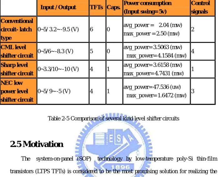
2.4 Comparison of Several Kind Level Shifter Circuits………...39
2.6 Summary and Conclusions……….………42
Chapter 3 Proposed Level Shifter Circuit Using
Low-Temperature Polycrystalline Silicon Thin Film
Transistors……….….43
3.1 Introduction………43
3.2 Proposed Level Shifter Circuit_A for Low Power Consumption………..44
3.3 Proposed Level Shifter Circuit_B for Low Input Voltage Driving………49
3.4 Proposed Level Shifter Circuit_C for Small Layout Area……….55
3.5 Fabrication Process and Measurement Result of the Proposed Level shifter Circuits..60
3.5.1 Measurement Result of the Proposed Level Shifter Circuit_A………62
3.5.2 Measurement Result of the Proposed Level Shifter Circuit_B………64
3.5.3 Measurement Result of the Proposed Level Shifter Circuit_C………66
3.6 Comparisons between the Proposed Level Shifter Circuits and Level Shifter Circuits……….69
3.7 Summary and Conclusions………71
Chapter 4 Summary and Conclusions………..73
References………...………75
Table Lists
Chapter2
Table 2-1 The design parameters of the conventional level shifter circuit. Table 2-2 The design parameters of the conventional level shifter circuit. Table 2-3 The design parameters of the NEC’s level shifter circuit. Table 2-4 The design parameters of the CML level shifter circuit. Table 2-5 Comparison of several kind level shifter circuits
Chapter3
Table 3-1 The design parameters of the proposed level shifter circuit_A. Table 3-2 The design parameters of the proposed level shifter circuit_B Table 3-3 The design parameters of the proposed level shifter circuit_C
Table 3-4 Compare simulation results of the proposed level shifter circuits and others level shifter circuits
Table 3-5 Compare measurement result of the proposed level shifter circuits and conventional level shifter circuit
Figure Captions
Chapter 1
Figure 1.1 CRT Vs. Flat Panel Figure 1.2 plasma display skeleton
Figure 1.3 Architecture of FED (field emission display)
Chapter 2
Figure 2.1 Block diagram of display panel. Figure 2.2 Architecture of the scan driver. Figure 2.3 Architecture of the data driver.
Figure 2.4 The schematic of the conventional level shifter circuit.
Figure 2.5 Measurement output characteristic of conventional level shifter circuit (use Table 2-1 condition).
Figure 2.6 Measurement output characteristic of conventional level shifter circuit (use Table 2-2 condition).
Figure 2.7 Simulation result of the output characteristic with power consumption relationship of conventional level shifter circuit
Figure 2.8 The schematic of the NEC level shifter circuit.
Figure 2.9 Simulation result of power consumption of NEC level shifter circuit Figure 2.10 Simulation result output waveform of NEC’s level shifter circuit. Figure 2.11 The schematic of the sharp level shifter circuit.
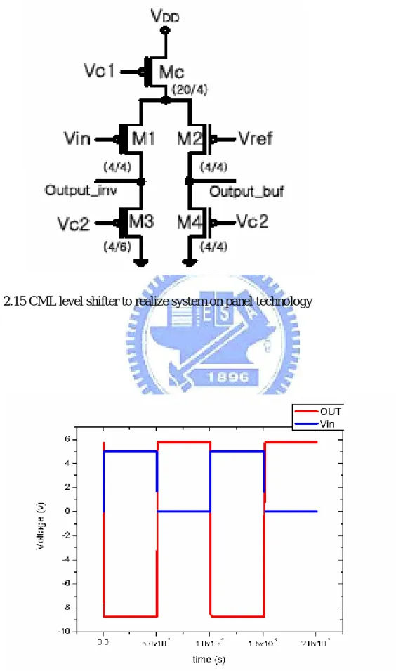
Figure 2.13 A CML level shifter circuit
Figure 2.14 Conventional static CMOS inverter type
Figure 2.15 CML level shifter to realize system on panel technology Figure 2.16 Simulation result of current mode logic level shifter circuit
Chapter 3
Figure 3.1 The schematic of the proposed level shifter circuit_A.
Figure 3.2 Simulation result of output signal, input signal and T2 NTFT gate voltage waveform.
Figure 3.3 Simulation result of level shifter circuit_A’s power consumption
Figure 3.4 Power consumption simulation result of proposed level shifter circuit_A compared to conventional level shifter circuit with different frequency Figure 3.5 Simulation result of VDD variation with input voltage increasing from 5 V to 10 V.
Figure 3.6 Simulation result of Vss variation with input voltage increasing from 5 V to 10 V.
Figure 3.7 The schematic of the proposed level shifter circuit_B.
Figure 3.8 Simulation result of output signal, input signal and T2 NTFT gate voltage waveform
Figure 3.9 Simulation result of level shifter circuit_B’s power consumption
Figure 3.10 Power consumption simulation result of proposed level shifter circuit_B compared to conventional level shifter circuit with different frequency.
Figure 3.11 Simulation result of VDD variation with input voltage increasing from 3.3 V to 10 V.
Figure 3.12 Simulation result of Vss variation with input voltage increasing from 3.3 V to 10 V.
Figure 3.13 The schematic of the proposed level shifter circuit_C. Figure 3.14 Simulation result of output and input waveform.
Figure 3.15 Simulation power consumption of proposed level shifter circuit_C. Figure 3.16 Power consumption simulation result of proposed level shifter circuit_C compared to conventional level shifter circuit with different frequency. Figure 3.17 Simulation result of VDD variation with input voltage increasing from 5 V to 10 V.
Figure 3.18 Simulation result of Vss variation with input voltage increasing from 5 V to 10 V.
Figure 3.19 The testing level shifter circuits were fabricated using a LTPS CMOS process
Figure 3.20 The measurement system for these testing level shifter circuits
Figure 3.21 The image of optical micrograph of the proposed level shifter circuit_A Figure 3.22 Measurement result of proposed level shifter circuit_A’s output waveform at frequency is 100 kHz.
Figure 3.23 Measurement result of propose level shifter circuit_A output waveform when input amplitude become 0 V to 3.3 V
Figure 3.24 The image of optical micrograph of the proposed level shifter circuit_B Figure 3.25 Measurement result of proposed level shifter circuit_B’s output waveform when input amplitude 5 V and frequency is 100 kHz.
Figure 3.26 Measurement result of proposed level shifter circuit_B’s output waveform when input amplitude 3.3 V and frequency is 100 kHz.
Figure 3.27 The image of optical micrograph of the proposed level shifter circuit_C Figure 3.28 Measurement result of propose level shifter circuit_C’s output waveform at
frequency is 100 kHz.
Figure 3.29 Measurement result of proposed level shifter circuit_C’s output waveform at frequency is 500kHz.
Figure 3.30 Measurement result of propose level shifter circuit_C’s output waveform at frequency is 1MHz.
Chapter 1
Background Introduction
1.1 Flat Panel Display Technology Overview
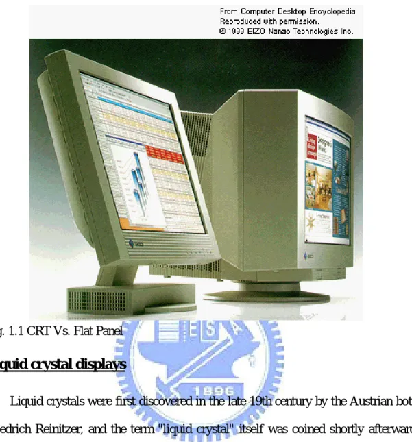
With a 100-year head start over competing screen technologies, the CRT is still a formidable technology. It's based on universally understood principles and employs commonly available materials. The result is cheap-to-make monitors capable of excellent performance, producing stable images in true color at high display resolutions. However, no matter how good it is, the CRT's most obvious shortcomings are well known:
• it sucks up too much electricity
• its single electron beam design is prone to mis-focus
• misconvergence and color variations across the screen
• its clunky high-voltage electric circuits and strong magnetic fields create harmful electromagnetic radiation
• it's simply too big see Fig. 1.1.
With even those with the biggest vested interest in CRTs spending vast sums on research and development, it is inevitable that one of the several flat panel display technologies will win out in the long run. However, this is taking longer than was once thought, and current estimates suggest that flat panels are unlikely to account for greater than 50% of the market before the year 2004.
Fig. 1.1 CRT Vs. Flat Panel
Liquid crystal displays
Liquid crystals were first discovered in the late 19th century by the Austrian botanist, Friedrich Reinitzer, and the term "liquid crystal" itself was coined shortly afterwards by German physicist, Otto Lehmann.
Liquid crystals are almost transparent substances, exhibiting the properties of both solid and liquid matter. Light passing through liquid crystals follows the alignment of the molecules that make them up - a property of solid matter. In the 1960s it was discovered that charging liquid crystals with electricity changed their molecular alignment, and consequently the way light passed through them; a property of liquids.
Since its advent in 1971 as a display medium, liquid crystal displays have moved into a variety of fields, including miniature televisions, digital still and video cameras and monitors and today many believe that the LCD is the most likely technology to replace the
CRT monitor. The technology involved has been developed considerably since its inception, to the point where today's products no longer resemble the clumsy, monochrome devices of old. It has a head start over other flat screen technologies [1.1]-[1.3] and an apparently unassailable position in notebook and handheld PCs where it is available in two forms:
• low-cost, dual-scan twisted nematic (DSTN)
• high image quality thin film transistor (TFT).
Plasma displays
Fig. 1.2 is show plasma display skeleton. Plasma Display Panels (PDPs) are like CRTs in that they are emissive and use phosphor, and like LCDs in their use of an X and Y grid of electrodes separated by an MgO dielectric layer and surrounded by a mixture of inert gases - such as argon, neon or xenon - to address individual picture elements.
They work on the principle that passing a high voltage through a low-pressure gas generates light. Essentially, a PDP can be viewed as a matrix of tiny fluorescent tubes which are controlled in a sophisticated fashion. Each pixel, or cell, comprises a small capacitor with three electrodes. An electrical discharge across the electrodes causes the rare gases sealed in the cell to be converted to plasma form as it ionises. Plasma is an electrically neutral, highly ionised substance consisting of electrons, positive ions, and neutral particles. Being electrically neutral, it contains equal quantities of electrons and ions and is, by definition, a good conductor. Once energised, the cells of plasma release ultraviolet (UV) light which then strikes and excites red, green and blue phosphors along the face of each pixel, causing them to glow.
Within each cell, there are actually three subcells, one containing a red phosphor, another a blue phosphor, and the third a green phosphor. To generate color shades, the perceived intensity of each RGB color must be controlled independently. While this is done in CRTs by modulating the electron beam current, and therefore also the emitted light intensities, PDPs accomplish shading by pulse code modulation (PCM). Dividing one field into eight sub-fields, with each pulseweighted according to the bits in an 8-bit word, makes it possible to adjust the widths of the addressing pulses in 256 steps. Since the eye is much slower than the PCM , it will integrate the intensity over time. Modulating the pulse widths in this way translates into 256 different intensities of each colour - giving a total number of color combinations of 256x256x256 = 16,777,216.
Fig. 1.2 plasma display skeleton
The fact that PDPs are emissive and use phosphor means that they have an excellent viewing angle and color performance. Initially, PDPs had problems with disturbances caused by interference between the PCM and fast moving pictures. However, this problem has been eliminated by fine-tuning the PCM scheme. Conventional plasma screens have traditionally suffered from low contrast. This is caused by the need to "prime" the cells, applying a constant low voltage to each pixel. Without this priming, plasma cells would
suffer the same poor response time of household fluorescent tubes, making them impractical. The knock-on effect, however, is that pixels which should be switched off still emit some light, reducing contrast. In the late 1990s Fujitsu alleviated this problem with new driver technology which improved contrast ratios from 70:1 to 400:1. By 2000 some manufacturers claimed as much as 500:1 image contrast, albeit before the anti-glare glass is added to the raw panels.
The biggest obstacle that plasma panels have to overcome is their inability to achieve a smooth ramp from full white to dark black. Low shades of grey are particularly troublesome, a noticeable posterised effect often being present during the display of movies or other video programming with dark scenes. In technical terms, this problem is due to insufficient quantisation, or digital sampling of brightness levels. It's an indication that the display of black remains an issue with PDPs.
Manufacturing is simpler than for LCDs and costs are similar to CRTs at the same volume. Compared to TFTs, which use photolithographic and high-temperature processes in clean rooms, PDPs can be manufactured in less clean factories using low-temperature and inexpensive direct printing processes. However, with display lifetimes of around 10,000 hours, a factor not usually considered with PC displays - cost per hour - comes into play. For boardroom presentation use this isn't a problem, but for hundreds of general-purpose desktop PCs in a large company it's a different matter.
However, the ultimate limitation of the plasma screen has proved to be pixel size. At present manufacturers can't see how to get pixels sizes below 0.3mm, even in the long term. For these reasons PDPs are unlikely to play a part in the mainstream desktop PC market. For the medium term they are likely to remain best suited to TV and multi-viewer presentation applications employing large screens, from 25in up to 70in.
For a number of years Fujitsu and Hitachi were the leading manufacturers of plasma displays. However, the number of patents issued for plasma display technology has surged in the last few years and now many large electronics companies believe PDPs are set to become a significant consumer product by 2002. Some estimate that worldwide shipments will have reached around 360,000 units by that time, representing a more than seven-fold increase since 1998.
PALCD
A peculiar hybrid of PDP and LCD is the plasma addressed liquid crystal display (PALCD). Sony is currently working, in conjunction with Tektronix, on making a viable PALCD product for consumer and professional markets.
Rather than use the ionisation effect of the contained gas for the production of an image, PALCD replaces the active matrix design of TFT LCDs with a grid of anodes and cathodes that use the plasma discharge to activate LCD screen elements. The rest of the panel then relies on exactly the same technology as a standard LCD to produce an image. Again, this won't be targeted at the desktop monitor market, but at 42in and larger presentation displays and televisions. The lack of semiconductor controls in the design allow this product to be constructed in low-grade clean rooms, reducing manufacturing costs. It's claimed to be brighter, and retains the "thin" aspect of a typical plasma or LCD panel.
Field Emission Displays
Fig. 1.3 is show FED architecture. Some believe FED (field emission display) technology will be the biggest threat to LCD's dominance in the panel display arena. FEDs capitalise on the well-established cathode-anode-phosphor technology built into full-sized CRTs using this in combination with the dot matrix cellular construction of LCDs. Instead
of using a single bulky tube, FEDs use tiny "mini tubes" for each pixel, and the display can be built in approximately the same size as an LCD screen.
Each red, green and blue sub-pixel is effectively a miniature vacuum tube. Where the CRT uses a single gun for all pixels, a FED pixel cell has thousands of sharp cathode points, or nanocones, at its rear. These are made from material such as molybdenum, from which electrons can be pulled very easily by a voltage difference, to strike red, green and blue phosphors at the front of the cell. Color is displayed by "field sequential color". The display will show all the green information first, then redraw the screen with red followed by blue.
Fig. 1.3 Architecture of FED (field emission display)
In a number of areas, FEDs look to have LCDs beaten. Since FEDs produce light only from the "on" pixels, power consumption is dependent on the display content. This is an improvement over LCDs, where all light is created by a backlight which is always on, regardless of the actual image on the screen. The LCD's backlight itself is a problem the FED doesn't have. Light from the backlight of an LCD passes through to the front of the display, through the liquid crystal matrix. It's transmissive, and the distance of the backlight to the front contributes to the narrow viewing angle. In
contrast, an FED generates light from the front of the pixel, so the viewing angle is excellent - 160 degrees both vertically and horizontally.
FEDs also have redundancy built into their design, most designs using thousands of electron emitters for each pixel. Whereas one failed transistor can cause a permanently on or off pixel on an LCD, FED manufacturers claim that FEDs suffer no loss of brightness even if 20% of the emitters fail. These factors, coupled with faster than TFT LCD response times and color reproduction equal to the CRT, make FEDs look a very promising option.
FEDs have their downsides though. One is that they are difficult to mass produce. While a CRT has just one vacuum tube, a SVGA FED needs 480,000 of them. To withstand the differences between the vacuum and external air pressure, a FED must be mechanically strong and very well sealed. Another problem is efficiency. To get enough electrons to produce adequate light, internal destruction of the emission layer is unavoidable. This begins with burn-in effects and eventually progresses to complete breakdown of the structure.
By the late 1990s, six-inch color FED panels had already been manufactured, and research and development on 10-inch FEDs was proceeding apace. However, since then the aforementioned barriershave caused the demise of many FED efforts. Variants of the technology still appear from time to time because as many companies continue to strive for new ways to compete with LCDs.
1.2 Overview of the Applications of Thin Film Transistors
(TFTs)
Thin-film transistors (TFTs) have been widely used in the electronic system applications in the past ten years. Depending on the different materials of active layer,
TT Tthin-film transistors (TFTs) can be mainly categorized to three types: TT Tamorphous
silicon thin film transistors (a-Si:H TFTs), polycrystalline silicon thin film transistors (poly-Si TFTs), and organic thin film transistors (OTFTs). Amorphous silicon thin film transistors (a-Si:H TFTs) were introduced in the 1970’s, which have been used in many applications such as solar cells [1.4], image sensors, printing heads, electronic copiers [1.5]-[1.7], especially in the applications of active matrix liquid crystal displays (AMLCDs) [1.8]-[1.10] and newly developed active matrix organic light emitting displays (AMOLEDs) [1.11]-[1.13]. In the AMLCDs, a-Si:H TFTs is used as the pixel switch placed at each pixel for addressing. While in the AMOLEDs applications, a-Si TFTs is used as the active device to provide driving current for illumination. Although a-Si TFTs has the advantage of low processing temperature (<350PPP
o
PPPC) to allow the use of cheap, mass-produced glass substrate. However, the low
carrier mobility of a-Si TFTs which is generally below 1cmPPP
2
PP P/V-s makes the difficulty
in realizing high resolution definition displays.
On the other hand, polycrystalline silicon (poly-Si) was used to be the active material of TFT for achieving higher performance in the 1980s. Poly-Si TFTs can be divided into two types according to the process temperature, which are high-temperature polycrystalline silicon TFT (HTPS TFT) and low-temperature polycrystalline silicon TFT (LTPS TFT). High- temperature poly-Si TFTs is fabricated by chemical vapor deposition (CVD) with processing temperature above 650PPP
o
approach requires an endured high-temperature substrate such as quartz, and this demand restricts to the small panel display such as projection display system which is inexpensive. Therefore, a low temperature process was investigated and progressed rapidly to be compatible with glass substrates for increasing economic benefits. Poly-Si TFTs fabricated with a maximum temperature below 600PPP
o
PP PC is so called
low-temperature polycrystalline silicon thin film transistors (LTPS TFTs). In the fabrication of LTPS TFTs, the crystallization of a-Si thin film is considered to be the most important process. Among various low temperature crystallization methods, the excimer laser crystallization (ELC) is considered to be the most promising approach to get high performance of the transistors compared with solid phase crystallization (SPC), metal induced crystallization (MIC) [1.14]-[1.15]. Low temperature poly-Si TFTs can be applied to image sensors [1.16], solar cells [1.17], 3-dimension ICs’ [1.18], and the most conspicuous application is the pixel element [1.19]-[1.20] and integrated peripheral circuits of active matrix liquid displays (AMLCDs) [1.21]-[1.23]and active matrix organic light emitting displays (AMOLEDs) [1.24]-[1.25]. Because of the higher carrier mobility and better reliability, LTPS TFTs offer the possibility for integrating the peripheral circuits with the pixel array on a single glass substrate to realize the final target of system-on-panel (SOP) which integrating the driver circuits, controller circuits, memory, central process unit (CPU), etc., and achieve the compact, highly reliable, and low cost display system.
In the recent years, organic thin film transistors (OTFTs) has attracted much interest due to the advantages of very low process temperature (<200PPP
o
PP PC) and easily
fabricated, therefore OTFTs can be fabricated on the flexible plastic substrate for low cost electronics applications. OTFTs can be applied to the switching devices for active matrix flat panel displays (AMFPDs) based on liquid crystal pixels(AMLCDs), organic light emitting diodes(AMOLEDs), or “electronic paper” displays
[1.26]-[1.27], additionally, sensors [1.28], low-end smart cards, and radio-frequency identification tags (RFIDs) consisting of organic integrated circuits. Although OTFT can be applied to large area, low-temperature processing, structural flexible, and low cost applications, this technology is not mature yet [1.29]. Many issues limit the applications of OTFT such as device stability and lifetime, and the most critical issue of OTFTs is the extremely low field effect mobility (typically <<1cmPPP
2 P PPVP PP -1 PP PsPPP -1 P PP)
compared to the a-Si TFTs and LTPS TFTs.
1.3 Integrated Driving Circuits of Displays
Low-temperature poly-Si (LTPS) thin-film transistors (TFTs) have been used as pixel and driving ICs in active matrix liquid crystal display (AMLCD) and active matrix organic light emitting diode display (AMOLED). To realize system-on-panel (SOP) or high performance TFTs on the isolated substrate attracts much more attention recently. There are many commercial products in small size flat display for mobile application using system-on-panel (SOP) technology, to get source driver and scan driver designed with TFTs. In recent year, more and more complex circuit blocks like digital analog converter (DAC), analog digital converter (ADC), timing controller, digital signal processing (DSP), microprocessor and DC-DC converter can be implemented by TFTs. In 2004, the first full-functional system panel was proposed by Sharp Corporation and Semiconductor Energy Laboratory Co,, where a CPU, a graphic controller, an audio circuit, a program ROM an audio ROM, various types of RAMs, a voltage generator, a clock generator, and the large- cale logic circuits comprising approximately 120,000 TFTs are monolithically formed on a glass substrate forming an LCD by using CG-Silicon technology. This concept of the system-on-panel (SOP) may compete with the concept of SOC in single crystal silicon technology, because SOC technology is requires large numbers of interconnections
between the panel and the peripheral circuits. Since off-panel connections have considered to be the most frequent cause of LCD failure, the system-on-panel (SOP) technology which omitting the usage of ICs and interconnections promise the LTPS-based products to be more reliable. However, reducing the number of external components and the connections to display enable to lower the cost of panel and a compact, light weight system can be achieved for better economic benefits.
Although the system display has been successfully demonstrated, the technology is not mature for mass production. In additional, the advantages of lower system cost and lower power consumption are not apparent nowadays. The properties of poly-Si TFTs are considered to be the key factors for the goal of system-on-panel, thus the disadvantages of electrical properties and the fabrication techniques of poly-Si TFTs must be improved to satisfy the requests for system on panel. Here, several critical issues and the research opportunities for developing system on panel are discussed in the following sections.
l
Issues of System-On-Panel
l UUUElectrical PropertiesUUU
At present, the performance of poly-Si TFTs is still much poor in comparison with conventional single-crystal MOSFETs such as lower carrier mobility, higher threshold voltage, larger subthreshold current and larger leakage current, etc. In order to achieve high speed and high driving capability of poly-Si TFTs, significant advances in carrier mobility are needed. As the carrier mobility is improved, the scale of the transistors can be reduced without sacrificing the driving current, thus high integrated density of transistors can be obtained for high resolution and more functions integrated display system. For the demand of low power consumption, low and centered (between n-tpe TFT and p-type TFT)
threshold voltage of poly-Si TFTs is needed. The high threshold voltage will result in relatively high voltage supply required to drive the circuits and dissipate high power.
The kink effect and hot carrier effect of poly-Si TFTs are also the critical problems in system display progressing. Kink effect of poly-Si TFTs causes the high value of output conductance and a strong dependence on bias condition [1.30] that will raise the difficulty in circuit design. For example, in analogue applications that will lead to a considerable reduction of the maximum attainable gain and reduces the common mode rejection ratio (CMRR), and result in increasing of power dissipation and slightly degrades the switching characteristics in digital circuits. Besides, the unsaturated I-V curve causes the problem in saturation voltage defined. The standard definition of saturation voltage is not applicable because a well-defined saturation does not exist. Hot carrier effect will cause the shift of threshold voltage, subthreshold swing, and mobility of poly-Si TFTs due to the carrier trapped in the Si/SiOBBB2 BBBinterface or carrier injection to the gate oxide. This will degrade the
reliability of poly-Si TFTs. Moreover, in order to reduce the kink effect and hot carrier effect, device with drain-engineering architecture or some circuit configurations (e.g. cascode, normally used to reduce the consequences of the kink on circuits) must be introduced. Thus the added steps of device process and excessive number of stacked devices are required which result in an increase in fabricated cost and power dissipation.
The device electrical properties play a key role in the performance of display, therefore, electrical characteristics of poly-Si TFTs must be further improved for meet the requirements of next system-on-panel (SOP) generation.
l UUUUniformityUUU
Over the past ten years, laser-based crystallization has been intensely studied and developed for poly-Si TFTs [1.31]-[1.34], and have been verified to be the excellent
technology with the ability to produce high quality poly-Si films [1.35]. Excimer laser crystallization (ELC) is the most commonly used method for mass production of LTPS TFTs. However, the narrow process window of laser energy density for producing poly-Si thin film is a critical issue for ELC LTPS TFTs. In order to crystallize large-grain poly-Si, the laser energy density must be controlled in the super lateral growth (SLG) region. Nevertheless, the pulse-to-pulse variations of excimer laser energy density and non-uniform laser beam profile causes the laser energy density not to be uniformly controlled in the SLG region across the large area. That result in random grain boundaries distributed in the channel region of LTPS TFTs between devices. As the channel dimensions continue to shrink, the uniformity behavior becomes more severe. The larger device-to-device variations will lead to many problems in real product applications.
l UUUDesign Rule ConsiderationUUU
The performance of poly-Si TFTs is inferior to that of conventional single crystallization Si MOSFETs at present. In order to keep compatible with large-area processing, relatively coarse design rules must been used in designing the poly-Si TFTs based circuits [1.36]. There are three reasons for this phenomenon. First of all, the restriction of photolithographic and processing for fabricating TFTs on the large-area substrate is severe. It is more challenging to scale down the device into the submicron dimension because of limitations in the resolution of lithography equipment. Second, the short-channel effects are relatively severe in poly-Si TFTs. As the dimension scaled down, the short-channel effects will intensely affect the device performance and make more difficulty in designing. Third, an AMLCD pixel typically requires a total voltage swing of about 10 V to encompass both the positive and negative driving polarities, and about 15 V supply voltage is needed by using poly-Si TFTs drivers. Therefore, the broader line width is
required.
In order to enhance the device performance, the dimension of poly-Si TFTs must be scaled down. For the development of more advanced panels systems, the dimension of channel must be shrunk to submicron dimension (<0.8um) to achieve high performance TFTs [1.37]. However, there are many challenges to scale down the device into the submicron dimension domain by current mass production technologies. Thus it requires the development and invention of new technologies of process and device.
l UUUPower ConsumptionUUU
Because of the higher threshold voltage, lower mobility, and loose design rule of poly-Si TFTs compared to single crystal Si MOSEFTs. It require higher supply voltage for sufficient driving capability of poly-Si TFTs, thus the power consumption of integrated driver circuits tends to be higher than that of single crystal silicon ICs. This tendency will increase as circuit-integration progresses. For example, in the case of QVGA (Quarter Video Graphics Array) LCDs, the power consumption of conventional TFT-LCD with external driver ICs ranges from 10 to 13 mW, while that of typical SOP LCDs with integrated driver circuits ranges from 20 mW upwards, which is more than twice of the power consumption of conventional TFT-LCDs [1.38].
Therefore, power reduction is one of the major challenges in further advanced SOP LCDs application. From the viewpoint of device electrical characteristics, low and centered (between nMOS and pMOS device types) threshold voltage with extremely small distribution is needed for meeting the requirement of low power consumption. Designing the driver circuits with simple configuration and less control signals are two a solutions from the designing aspect. Furthermore, modified driver architecture and lowered the line resistance and parasitic capacitance are also the efficient methods to reduce the power
consumption.
l UUUYieldUUU
At present, the fabrication cost of low-temperature poly-Si TFTs is higher than that of amorphous silicon TFTs because of more process steps and more expensive equipments. The reduction of external component cost has been offset by the higher fabrication cost in many commercial applications, resulting in higher display prices. Besides, the narrow process window of laser crystallization technology, and additional steps or more complex texture employed to achieve high performance poly-Si TFTs (ex. drain engineering for reducing the kink effect and hot carrier effect, additional steps or equipments for crystallization to get high carrier mobility) will also reduce the production yield rate. Therefore, how to obtain high manufacturing yield is really important for real production applications.
l
Research Opportunities for Realizing System-On-Panel
To achieve the goal of system-on-panel, the improvements at various levels are required to solve several issues as discussed above. This can be achieved from three aspects: materials and process technology, device structure, and circuit design.
l UUUMaterials and Process Technology
New elemental process technology is needed for the formation of high quality critical
layers, such as the active and the gate-insulator layers of poly-Si TFTs. In the area of active layer, high quality poly-Si microstructure is needed to increase device
performance. The crystallization process is a very critical step of the fabrication process for TFTs, because it needs to satisfy the requirements on trade-off considerations including material quality, fabrication cost and thermal-budget constraints imposed by the display substrate. The key points for further improved poly-Si crystallization technology are high electrical performance and good uniformity which can be achieved through enlarging grain size, reducing the defect densities, getting good grain orientation and location control. Several advanced crystallization technology has been proposed to achieve large grain size or location controlled poy-Si film such as the “Continuous Grain Silicon (CG Silicon)” technology by Shrap Corporation [1.39]-[1.40], “Selectively enlarging laser crystallization (SELAX)” technology by Hitachi, Ltd. [1.41]-[1.42], or “comb-shaped excimer laser annealing” technology by NEC Corporation [1.43].
In terms of gate insulator layer, there are several requirements in thickness and film quality - i.e. fixed and interface trap density, reliability against electrical stress. GI thickness reduction is necessary to get a TFT gate length in the submicron range. As GI thickness decreases, issues of step coverage become increasingly more severe. Current gate insulator technology is based on PECVD TEOS-SiO2, but this technology seems incapable of overcoming the challenge with the gate insulator thickness gradually decreasing to 50 nm and beyond. In order to maintain high quality for increasingly thinner gate insulator layer, new technology must be introduced.
l UUUDevice Architecture
Modified device architectures must complement and customize device performance according to required function. Improvements in the device architecture are vital in two aspects: (1) enable the fabrication of submicron channel dimensions with technology compatible with LCD manufacturing and (2) provide an additional way to complement
material quality and compensate the variation of material properties in the critical layer for supplying additional controls for system optimization. But it must conform to the requirement of low cost, thus without extra process step (ex. additional steps for drain engineering or integration of low-voltage and high-voltage TFTs) is also taken into consideration.
l UUUCircuit Design
In additional to improved process technology and device structure, improvements from the circuits design concept offer another solution to realize the goal of system-o n-panel. For example, analog buffer which is indispensable to driving large load capacitance of the panel will suffer from large offset voltage and huge output variation due to the high threshold voltage and large device-to-device variation of poly-Si TFTs. Precise circuit design is employed to deal with the output offset voltage and eliminate the output variation of the buffer circuits through the appropriate circuit architecture and driving scheme. To ensure designing accurately of circuits, suitable device model and exact device parameters are required. It is important to develop accurate models of poly-Si TFTs for circuit simulation and design.
Chapter2
Overview of All Kinds of Level Shifter
Circuits Using LTPS TFTs for Active Matrix
Displays
---
2.1 Background Introduction
Researches on “system-on-panel” technology have attracted much attention at present because it provides a chance to realize a compact, light weight, high reliability, and low cost display [2.1]-[2.3]. Low-temperature polycrystalline silicon thin film transistor is considered to be the best candidate for portable displays due to the low temperature process, high carrier mobility and the compatibility to CMOS technology, which allow the integration of the driver circuit and even more complicated parts such as controller circuits, random access memory (RAM), and central processing unit (CPU) with pixel circuits on a single glass substrate.
To realize integrating driving circuits using LTPS TFTs, level shifter circuit are indispensable for data driver is to pull high voltage for digital signal become analog signal and level shifter in scan driver is pull high voltage over ten voltage to turn on TFTs on scan line, moreover turn off TFTs on scan line maintain minimum leakage current and consequently pull down voltage over negative five voltage. However, the high threshold
voltage, low mobility, and loose design rule of LTPS TFTs, lead to poor output swing accuracy and high power consumption. Therefore, many researches employing LTPS TFTs have been tried carry out level shifter circuit with high output swing and low power consumption.
In this chapter, the circuit configuration, operating sequence, advantages and disadvantages of all types of LTPS TFT level shifter circuits are introduced. The works principles of all types LTPS TFT level shifter circuits with configuration will be described in detail in this chapter. Furthermore, the output characteristics of the all kind of level shifter circuits are also discussed in this chapter.
l Architecture of AMLCD Driver
The block diagram of AMLCD display panel is shown in Fig. 2.1. The periphery circuits blocks of LCD panel are composed of scan driver, data driver, timing controller, DC/DC converter, gamma reference voltage driver, common voltage driver (Vcom driver). The timing controller decodes the output waveform to generate control signals at corresponding time, which is responsible for controlling the behavior of scan driver and transmitting the RGB (red, green, and blue) signals to the data driver. A DC-DC converter steps up a single externally supplied voltage to various higher level voltages (ex. VDD to 2VDD, 3VDD positive output voltage, and -2VDD, -3VDD negative output voltage) which provide the power supply voltage to the timing controller, interface circuit, source driver, gate driver, reference voltage driver and common voltage driver [2.4]-[2.5]. The gamma reference voltage driver is used to provide the various gamma reference voltages to the digital-to-analog converter (DAC) circuits. The common voltage driver is used to provide the common electrode voltage for the panel. Besides, the scan driver and data driver will be further discussed in the following section.
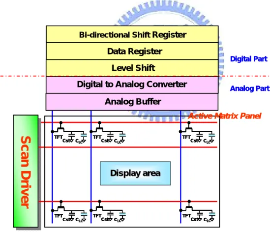
l Scan Driver
The scan drivers generate the scan pattern and turn on each scan line sequentially. The architecture of source driver is shown in Fig. 2.2. It consists of shifter register, level shifter, and output buffer. The shift register is used to store digital input signal and transit them to the next stage, which generates sequential scan pulse for scan line according to the timing clock. The function of the level shifter is to translate the digital signal to a higher level voltage because the higher voltage is needed to turn on the switch element of the active pixel. Since the scan lines can be modeled as RC (resister and capacitor) ladder, the output buffer is indispensable to drive the RC loading.
l Data driver
Fig. 2.3 shows the architecture of data driver which mainly contains shifter register, data register, level shifter, digital to analog converter (DAC) and output buffer. The first three stages are categorized as digital part, and the other two stages are belonged to analog part. The shift register generates pulse signal for video signal sampling according to the clock signal and transmit the pulse digital RBG signals to the next stage [2.6]. The data register receives the serial data signal and transmits them in parallel. The function of the level shifter is the same as the one used in the scan driver. It is applied to converter the digital RGB signal to a higher level voltage for data driver [2.7]. Because the data signal is transmitted in the digital interface, the digital to analog converter (DAC) is needed to convert the digital RGB video data into analog data signal for displaying the gray level [2.9]-[2.10]. Finally, the selected video data is transmitted to the data line after changing impedance in the output buffer. The purpose of output buffer is to assure the active pixels
can be driven into a desired gray level. When the digital to analog converter is insufficient for driving the large loading of data line, the output buffer is used to enhance its driving capability. As the output buffer is applied, the DAC will charge a smaller loading of output buffer instead of a larger loading of data line. Thus, the desired data signal can be transmitted to the active area accurately. Because the LCD panel usually has large loading, especially in larger panel or higher resolution display, the analog buffer is essential to drive the large loading of the data lines.
Fig. 2.2 Architecture of the scan driver.
S
c
a
n
D
ri
v
e
r
TFT Cst CLC TFTCst CLC TFT Cst CLC TFT Cst CLC Display area Display area TFT Cst CLC TFT Cst CLCActive Matrix Panel Bi-directional Shift Register
Data Register
Analog Buffer
Digital to Analog Converter Level Shift Analog Part Digital Part
S
c
a
n
D
ri
v
e
r
S
c
a
n
D
ri
v
e
r
TFT Cst CLC TFT Cst CLC TFT Cst CLC TFTTFTTFTCstCstCst CCCLCLCLC TFT Cst CLC TFT Cst CLC TFT Cst CLC TFT Cst CLC TFT Cst CLC TFT Cst CLC Display area Display areaDisplay area Display area TFT Cst CLC TFT Cst CLC TFT Cst CLC TFT Cst CLC TFT Cst CLC TFT Cst CLCActive Matrix Panel Bi-directional Shift Register
Bi-directional Shift Register Data Register Data Register
Analog Buffer Analog Buffer
Digital to Analog Converter Digital to Analog Converter
Level Shift Level Shift
Analog Part Digital Part
2.2 Design Considerations of Level Shifter Circuit
To design the level shifter circuits for the data driver and scan driver of flat pane display, there are several critical issues to be considered. These include high efficient level shifter, threshold voltage variation compensation, low power consumption and layout area.
l Level Shifter with High Efficiency
The output settling time for the data drivers and scan driver must be settled enough to transfer the data signals into the pixels within a line time. Therefore, the level shifter circuits of the data driver and scan driver must quickly charge or discharge the next loading. Especially in the larger panel area and higher resolution display, the line time becomes shorter while the loading of data line and scan line is large. High driving capability of the level shifter circuit is needed to achieve fast transition time and to get sufficient capability for driving large loading of data lines and scan line.
l Threshold Voltage Variation Compensation
LTPS TFTs suffer from huge device-to-device variations due to the pulse-to-pulse variation of laser energy density and random distribution of grain boundaries, such poor uniformity makes the difficulty to fully integrate driving circuit using LTPS TFTs. Although LTPS TFTs have threshold voltage variation lead to level shifter circuits output swing variation, but in general case, scan driver and data driver last section output buffer aimed at threshold voltage variations.
l Low Power Consumption
The power consumption of poly-Si TFT integrated circuits tends to be higher than that of single-crystalline silicon ICs because of inferior electrical characteristics of poly-Si TFT such as higher threshold voltage, lower carrier mobility. For the expanding market of mobile and portable production, the demand of power dissipation is increasing. Since several hundreds of level shifter circuits are needed in the LAAT (line at a time) driving architecture, large static power is dissipated of level shifter circuit. Therefore, it needs to design an level shifter circuit with low power consumption.
l Small Layout Area
For the LAAT (line at a time) driving architecture, one level shifter circuit is needed for each column line. Thus, several hundreds of level shifter circuit are needed in active matrix display. As the resolution is higher and higher in the future, the amount of level shifter circuit is increasing and larger area will be occupied. Moreover, a data driver and scan driver should fit in one pixel pitch, and circuit layout area is limited. Therefore, the simple configuration and few transistors are pursued for high-resolution display.
2.3 All Kinds of Level Shifter Circuits
In previous section, critical issue of level shifter circuit was discussed. There different structure of level shift circuits for different critical issue have different methods, while level shifter circuit configuration, operating sequence, advantages and disadvantages of all types of low-temperature poly-Si (LTPS) thin-film transistors (TFTs) level shifter circuits are introduced.
2.3.1 Conventional Level Shifter Circuit
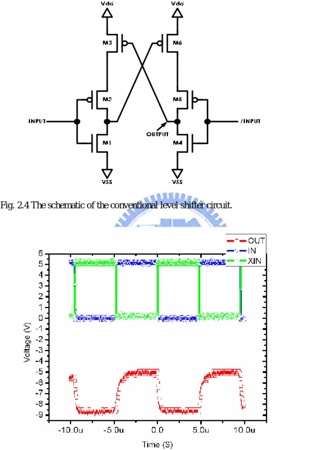
Fig. 2.4 is show a conventional level shifter circuit, the level shifter circuit composed of a positive power voltage VDD, a negative power voltage GND, an input signal “Input”, an output signal “Output”, p-channel TFTs M2, M3, M5 and M6 and n-channel M1 and M4.The conventional level shifter circuits operation have two step, first step as Input is logic0, at the present M2, M3, M4 TFTs is turn on, while M1, M5, M6 TFTs is cut off, and output voltage is discharged to Vss. The second step as Input is logic1, at the present M1, M5, M6 TFTs is turn on, while M2, M3, M4 TFTs is cut off, and output precharged up to Vdd. Fig. 2.5 and Fig. 2.6 are measurement output characteristic of conventional level shifter circuit, their measurement condition is like Table 2-1 and Table 2-2 respectively. In direct current analysis, conventional level shifter circuit have more static power consumption and dynamic power consumption from Fig. 2.7 we can observed, the main factor is M1 and M4 TFTs are not enough cut off exactly , when Input is logic0 with /Input is logic1 respectively. This main factor lead to some leakage current pass M1 and M4 TFTs path to Vss, except caused more power consumption and output waveform characteristic curve have poor amplitude, need increase M5 and M6 TFTs size to solve this problem. But increase M5 and M6 TFTs size still not solve this problem exactly, because restricted by circuit Architecture.
Fig. 2.4 The schematic of the conventional level shifter circuit.
Fig. 2.5 Measurement output characteristic of conventional level shifter circuit (use Table 2-1 condition).
Table 2-1 The design parameters of the conventional level shifter circuit.
Fig. 2.6 Measurement output characteristic of conventional level shifter circuit (use Table 2-2 condition).
Signal
IN
0v ~5v
Vdd
10 V
Vss
-10 V
Frequency
100 kHz
Devices T1.T4 (N-type) T2.T3.T5.T6 (P-type) 8μm/8μm 8μm/8μmTable 2-2 The design parameters of the conventional level shifter circuit.
Fig.2.7 Simulation result of the output characteristic with power consumption relationship of conventional level shifter circuit
Signal
IN
0 V ~5 V
/IN
5 V~0 V
Vdd
10 V
Vss
-10 V
Frequency
100 kHz
Devices
T1.T4
(N-type)
T2.T3
(P-type)
T5.T6
(P-type)
8μm/8μm
20μm/8μm
150μm/8μm
2.3.2 NEC Low-Power Level Shifter Circuit
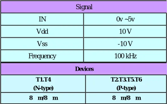
The circuit configuration of NEC low power level shifter [2.11] is shown in Fig. 2.8. It is composed of a positive power voltage VDD, a negative power voltage Vss a one sampling capacitor C1, four TFTs, output loading (capacitor C2) and three control signals (CLK, XCLK, DATA). Level shifter circuit operation have two state, first step is set-up state and second is evaluation state. When set-up state sampling capacitor C1 stores input data of 3 V amplitude, and capacitor C2 is precharged up to +10 V through P1 while N3 is in a cut-off state. When second step evaluation state sampling capacitor C1 maintains its data voltage storage. P1 is in a cut-off state, and one of two operations is performed depending on the C1 voltage. For C1=0 V, C2 maintains 10V since N2 is in a cut-off state and for C1=3 V,C2 discharges to -10 V since N2 and N3 are conductive. The level shifter circuit utilizes N1, N2 device and DATA control signals and sampling capacitor C1 to restrain static power consumption. This advantage of is level shifter circuits is to utilizing N1, N2 device and DATA control signals and sampling capacitor C1 to restrain static power consumption from Fig. 2.9 we can observe, but drawback is need more control signals increase complexity, moreover sampling capacitor C1 increase layout area size, and if reduce input swing cause have poor output amplitude. The circuit output characteristic and simulation condition of NEC low power level shifter is show in Fig. 2.10 and Table 2.3 respectively.
Fig. 2.8 The schematic of the NEC level shifter circuit.
Fig. 2.10 Simulation result output waveform of NEC’s level shifter circuit.
Table 2-3 The design parameters of the NEC’s level shifter circuit.
Signal
IN
0 V ~10 V
XIN
10 V~0 V
Vdd
10 V
Vss
-10 V
Data
0 V~3 V
Frequency
100 kHz
Devices
N1.N2
(N-type)
N3
(N-type)
P1
(P-type)
C1
8μm/8μm
40μm/8μm
8μm/8μm
1pf
2.3.3 Sharp Level shifter Circuit
Fig. 2.11 shows a level shifter circuit [2.12]. The level shifter circuit composed of a positive power voltage VDD, a negative power voltage GND, an input signal IN, an output signal OUT, a capacitor C11, p-channel TFTs p11 and p12 and n-channel n11 and n12. Fig. is constituted by a bias voltage setting section constructed of the positive power voltage VDD, negative power voltage GND, p-channel TFT p11 and the n-channel TFT n11 and amplifier circuit section constructed of the positive power voltage VDD, negative power voltage GND, p-channel TFT p12 and n-channel TFT n12. The input signal IN is capacitively coupled with the capacitor C11 and inputted to the input terminal of the amplifier circuit section. In this case, depending on a bias voltage determined on an ON-state resistance ratio between the p-channel TFT p11 and the n-channel TFT n11 (this voltage being defined as Vb), the voltage level of swing of the input signal IN is shifted to the bias voltage Vb although the amplitude does not change. That is, by correctly setting the bias voltage Vb, the amplifier circuit section can be normally. Then, in the amplifier circuit section, the p-channel TFT p12 is turned off and the n-channel TFT n12 is turned on when the input signal IN has high level, as a consequence of which the negative power voltage GND is outputted form the output terminal of the amplifier circuit section. The p-channel TFT p12 is turned on and the n-channel TFT n12 is turned off when the input signal IN has low level, as a consequence of which the positive power voltage VDD is outputted from the output terminal of the amplifier circuit section.
Fig. 2.12 shows a relation between the input and output of the level shifter circuit. If the absolute value of the threshold voltage of the p-channel TFT constituting the level shifter circuit become smaller than the absolute value of the threshold voltage of the n-channel TFT, then the input-to-output voltage characteristic of the amplifier circuit section comes to
have a characteristic curve of the waveform c, and the operation point is shifted to the positive power voltage VDD side. In this case, if the signal to be inputted to the input terminal of the amplifier circuit section remain the signal inb, then a signal outc is outputted form the output terminal of the amplifier circuit section, meaning that sufficient amplitude conversion is not effected. However, If the absolute value of the threshold voltage of the p-channel TFT constituting the level shifter circuit become smaller than the absolute value of the threshold voltage of the n-channel TFT, then the ON-state resistance value of the p-channel TFT p11 becomes smaller than the ON-state resistance value of the n-channel TFT n11. Therefore the bias voltage determined by the bias voltage setting section is shifted form Vb to the positive power voltage VDD side to become Vc, and the signal to be inputted to the input terminal of the amplifier circuit section becomes a signal inc. As a result, the signal outb is outputted from the output terminal of the amplifier circuit. Conversely to the above, if the absolute value of the threshold voltage of the p-channel TFT constituting the level shifter circuit become grater than the absolute value of the threshold voltage of the n-channel TFT, then the ON-state resistance value of the p-channel TFT p11 becomes grater than the ON-state resistance value of the n-channel TFT n11. Therefore the bias voltage determined by the bias voltage setting section is shifted form Vb to the negative power voltage GND side to become Va, and the signal to be inputted to the input terminal of the amplifier circuit section becomes a signal ina. As a result, the signal outb is outputted from the output terminal of the amplifier circuit section instead of a signal outa.
This level shifter circuits have two drawbacks. One is c11 capacitance need over 1uF, that is increase layout area size. Another drawback is about static power consumption , because n-channel n11 and p-channel p11 always turn on caused Vdd discharged to Vss leading large power consumption.
Fig. 2.11 The schematic of the sharp level shifter circuit.