國 立 交 通 大 學
顯示科技研究所碩士班
碩士論文
不同材料的背電極對溶液製程
金屬氧化物薄膜電晶體之特性影響
Solution-processed metal-oxide thin-film transistor
with floating capping materials
研 究 生: 王 辰
指導教授:冉曉雯 教授
不同材料的背電極對溶液製程
金屬氧化物薄膜電晶體之特性影響
Solution-processed metal-oxide thin-film transistor
with floating capping materials
Display Institute
National Chiao Tung University
研 究 生: 王 辰 Student : Cheng Wang
指導教授: 冉曉雯 教授 Advisor : Prof. Hsiao-Wen Zan 國立交通大學
顯示科技研究所 碩士論文
A thesis
Submitted to Institute of Display Institute
College of Electrical Engineering and Computer Science National Chiao Tung University
in partial Fulfillment of Requirements for the Degree of Master
in Display Institute
June 2011
Hsinchu, Taiwan, Republic of China
I
不同材料的背電極對溶液製程
金屬氧化物薄膜電晶體之特性影響
研究生:王 辰 指導教授:冉曉雯 教授
國立交通大學
顯示科技研究所碩士班
Chinese Abstract
中文摘要
溶液製程的金屬氧化物薄膜電晶體近年來受到大家的重視,一方面是因為其能 隙很大且可以形成一層非常透明的薄膜;另一方面是其製程的成本是非常低廉的。然 而,其過高的製程敏感性和元件操作穩定性及需要在高溫中退火限制了其在徹底商 業化的進程。本論文從一開始如何做出一個金屬氧化物電晶體開始講起,並且為了 要改善元件的電性,嘗試了不同的金屬氧化物(ZnO,GZO,IGZO),且改變不同金 屬前驅物混合的比例,以求達到一個極佳化的電性。此外,為了得到一個大於 0V 的臨界電壓,我們嘗試對混合的金屬氧化物前驅物溶液進行處理,譬如在溶液進行 膠融的時候利用磁石高溫攪拌,加速前軀物的反應,或是在手套箱中進行攪拌,結 果發現我們可以利用控制上述的變因來偏移臨限電壓。為了能使整個製程控制在較 低的溫度,我們也對上述不同的金屬氧化物進行了不同的退火溫度測試並製成了薄II 膜電晶體並進行電性比較,發現還是 IGZO 薄膜電晶體在低溫的退火環境下還能量 測到較好的電性。 我們使用了上述得到的最佳化的 IGZO 薄膜電晶體進行了第二段的測試。從濺 鍍 a-IGZO 薄膜電晶體的研究得知,在元件的背表面覆蓋上某些材料會導致遷移率 大幅的提升。我們也期待在溶液製程的的 IGZO 薄膜電晶體也能得到這樣的結果。 我們設計不同的覆蓋比率對標準 IGZO 薄膜電晶體覆蓋了 SiO 測試,對於 IGZO 經 過 600℃的高溫退火環境的元件,電子遷移率真的如我們所期望的大幅的提升了, 從~2 cm2V-1s-1改善到~15 cm2V-1s-1。在較低的退火環境下(400℃),遷移率也有所 改善,從~0.1 cm2V-1s-1改善到~1 cm2V-1s-1。 除了覆蓋 SiO 外,我們也在元件上覆蓋孤立的鈣電極,結果發現了元件遷移率 除了也會有很顯著的提升,臨界電壓會往負大幅的偏移。我們對覆蓋這兩種不同的 材料所造成元件的影響做了一些假設,並且希望在未來的研究可以得知其遷移率大 幅改善的原因。 這篇論文確實提供了溶液製程金屬氧化物電晶體的方法與特性解釋,並可做為 對後來研究的一個相當值得參考的資料。
III
Solution-processed metal-oxide thin-film transistor
with floating capping materials
Student:Cheng Wang Advisor:Prof. Hsiao-Wen Zan
Display Institute
National Chiao Tung University
Abstract
Solution-processed indium-gallium-zinc-oxide TFTs had been studied for many
years. The most attractive is the low cost fabrication processes, high transparency and
large band gap. However, the performance on solution processed metal-oxide TFTs is
not stable, it need high annealing temperature (>400℃) to achieve high performance
device characteristics. Therefore, decreasing the annealing temperature to obtain high
performance solution processed metal-oxide TFTs is an important issue, some people
proposed that increasing the Gallium concentration will decrease the annealing
temperature form >400℃ to 200℃, and increase the annealing time will achieve high
performance in low annealing temperature.
In this study, we fabricated the conventional thin-film transistor with different
IV
achieve high mobility, bottom-gate metal-oxide TFTs with low annealing temperature,
we tested some methods such as adjusting different composition of metal-oxide
semiconductor and adjusting different stirring temperature. As a result, we found the
best electric characteristic on IGZO thin-film transistor and the annealing temperature
could decrease to low than 400℃ and exhibited a mobility of 0.1 cm2V-1s-1.
Additionally, we used above best result to cap SiO on the back channel of
metal-oxide film, and we found that the mobility increased obviously with increasing
the percentage of capping ratio. We also discussed some possible physical mechanism
on it. The optimized electric characteristic of indium-gallium-zinc-oxide TFT was
attained a mobility around 15 cm2V-1s-1, sub-threshold swing of 0.4 V/decade, on/off
ratio of×106 and VT of 0.11 V in high annealing temperature (600℃); we could get a
mobility of 1 cm2V-1s-1 in low annealing temperature (400℃).
The same result was found in dual gate thin-film transistor with capping Calcium.
The physical mechanism was different from capping SiO.
Here we discussed a lot of possible mechanisms of indium-gallium-zinc-oxide
thin-film transistors and it’s useful for future developing for high performance
V
Acknowledgement
廢廢的我要走了,相比我意氣風發的來。我緩緩的招手,告別兩年的學涯。 那壬冉的甘苦歲月,就這樣輕巧從我的腋下溜走了。遺留下來的只是那充滿 著青春的汗臭味跟肥碩的回憶。遙想當年,那一個青澀的小蘿蔔頭就這樣蹦蹦跳 跳的來到了這一個大家庭,在此我也度過了我那充滿傳奇的兩年生活。感謝冉曉 雯教授這兩年多的指導,帶給我非常多新觀念的衝擊,此外也讓我領悟一些人生 大道理,而且能認清自己的弱點,勇敢面對恐懼。能坦然接受失敗,驕傲不屈。 再來,需要感謝的當然就是武衛跟長紘這兩位學長。武衛學長在這兩年內給 我許多實用的建議,並且在我最需要溫暖的時候給予我最大的支援。長紘學長在 實驗的積極態度也惠我良多。我在這兩位學長的引領之下,擁有積極的求知慾。 此外,長紘學長也是實驗室的開心果,他擁有的極度自信真是令我大開眼界,值 得我輩效法。此外,我還要另外感謝兩個人,家新和洪正。由其是家新,讓我在 轉換跑道由 SCLT 到 TFT 的時候能毫無困難的就能銜接上去。身為人生奮鬥組 的哥兒們,洪正在趕論文的五、六月給我一些很溫暖的鼓勵,當我內心非常徬徨 的時候,看到你在 Battle,馬上就能讓我心坎注入了一劑強心針,讓我備感溫馨。 祝福你在博班的道路上能走得順順利利,跟長紘一起共創 Nature 王朝。(小得沒 辦法跟隨在兩位驥尾,即日起即將投效軍旅,親赴前線,在此深表遺憾) 還要感謝一些實驗室的前輩與同儕與學弟們,讓我能在做苦悶的實驗環境中 多點生活樂趣。也要感謝一些大學的同窗好友與同鄉,當我遭遇挫折時,我還可VI 以回去找你們取暖。沒有你們的背後鼓勵,這兩年的時光可是很難熬的。 最後我想要抒發內心的想法。小時候,看到書上描述著大漠風光的壯麗,也 癡心妄想未來要去草原放牧。現在的我雖然朝理想越來越遠,但是我希望自己心 裡還是保持著那一份願望,希冀自己有朝一日能達成。我也希望在人生的道路上, 自己不會對自己所做的任何決定感到後悔。曾經,你差點就想要放棄了,但你畢 竟還是把他堅持住,這就對了。路是人走出來的,未來是人闖出來的。即使在未 來的道路上也許有很多荊棘刺人,但我還是相信你和你那非常聰穎的灰色腦細胞, 強弩煙飛滅。加油吧,boy! 欲知未來如何,請待來年分解。 ppwang 2011.07.18 筆
VII
CONTENTS
CHINESEABSTRACT………...……….….….Ⅰ ENGLISH ABSTRACT…………...……….………….Ⅲ ACKNOWLEDGEMENT……….………Ⅴ CONTENTS….………...………….………..… Ⅶ FIGURE CAPTIONS……….…Ⅹ TABLE CAPTIONS…………...……….……….……. XIIICHAPTER 1 INTRODUCTION……..……….….……1
1-1 An overview of metal-oxide semiconductors thin-film transistors…….…….1
1-2 Carrier transmission mechanism of metal-oxide semiconductors………..…..2
1-3 Annealed temperature for metal-oxide film……….……….4
1-4 Formation Mechanism of indium-gallium-zinc-oxide thin-films……….4
1-5 Materials-capped for metal-oxide semiconductor thin-film transistors….…...6
1-6 Thesis outline……...………6
FIGURES of CHAPTER 1……….……….…7
CHAPTER 2 EXPERIMENT SETUP………..……….9
2-1 Experimental procedure……….…..………9
VIII
2-1.2 Materials-capped (SiO, Calcium)..……….……….11
2-2 Fabricated of sol-gel metal-oxide precursors……….……..12
2-2.1 ZnO precursors………..………..…………12
2-2.2 GZO precursors……….……….………….13
2-2.3 IGZO precursors……….13
2-3 Operation mechanism and parameter of transistors…………...…..…………13
2-3.1 Operation mechanism………...…..………13 2-3.2 Linear regions……….14 2-3.3 Saturation regions………..………….13 2-3.4 Mobility…..………15 2-4 Experimental instruments………16 2-4.1. Spin coater………...………..…………16 2-4.2. Thermal evaporation……….………16
2-4.3. Four-point probe resistivity measurement………16
2-4.4. Atomic force microscope measurement………..……..17
FIGURES of CHAPTER 1………..……….….18
CHAPTER 3 RESULT and DISCUSSION………...………..….21
3-1 The leakage of solution-processed metal-oxide TFTs……….…………22
IX
3-2.1 Zinc-oxide TFTs characteristics in different precursor solution stirred
atmosphere……….……….……….22
3-3 Bottom gate top contact gallium-zinc-oxide TFTs………..………25
3-4 Bottom gate top contact indium-gallium-zinc-oxide TFTs……….…26
3-4.1The precursor solutions in different stirring atmosphere………27
3-4.2 The different annealing temperature for IGZO (1:2:2) TFTs………..…28
3-4.3 The influence of stabilizer in indium-gallium-zinc-oxide TFT….…….29
3-5 The standard thin-film transistor with materials-capped………...……30
3-5.1 SiO-capped on standard indium-gallium-zinc-oxide thin-film transistor………..30
3-5.2 Calcium-capped onto standard indium-gallium-zinc-oxide thin-film transistor………..………..……….………….32
FIGURE of CHAPTER 3……….….34
CHAPTER 4 CONCLUSIONS and FUTURE WORK………….……..…..…….48
4-1 Conclusion………...48
4-2 Future work………..……….…..49
CHAPTER 5 APPENDIX……….……….……...50
(A) Top gate bottom contact TFT with whole SiO-capped………50
X
Figure Captions
Fig. 1.1 The carrier transport paths in covalent semiconductors and AOSs [12]..7 Fig. 1.2 TG-DSC curves of IGZO sol-gel solution [7]……….……..8 Fig. 1.3 Conventional bottom gate metal-oxide thin-film transistor……...………8 Fig. 1.4 Materials-capped metal-oxide thin-film transistor………..8 Fig. 2.1 Metal-oxide TFTs fabrication process………18 Fig. 2.2 Materials-capped TFTs structure………...……….…20 Fig. 2.3 Chemical structures of the (a) 2-methoyxethanol (b) monoethanolamine (c) the chemical properties……….……20 Fig. 3.1 The ID-VG curve of the ZnO TFTs with and without wet etching………34
Fig. 3.2The ID-VG curve and -VG characteristics of the ZnO TFTs by
adjusting precursor solution in different atmosphere. (The channel width /channel length, W/L=1000μm /200μm)………...34 Fig. 3.3 The ID-VG curve and -VG characteristics for different channel layers
of the ZnO TFTs.(The precursor solution was stirred in glove box at RT)
(The channel width /channel length, W/L=1000μm /200μm)……….35 Fig. 3.4 AFM images of different precursor solutions stirring atmosphere(a)stirred slightly (b)stirred vigorously (c) stirred slightly at 60..….36 Fig. 3-5 The ID-VG curve of the GZO TFTs according to different
XI
Ga-incorporated solutions. (the solution stirred in air at RT)(The channel width /channel length, W/L=1000μm /200μm)...……….……….…..36 Fig. 3.6 The ID-VG curve and -VG characteristics for different mixed ratio
(1:1:2 and 1:2:2) of the IGZO TFTs in different precursor condition.(The channel width /channel length, W/L=1000μm/200μm)..……….……37 Fig. 3.7 The ID-VG curve and -VG characteristics for IGZO(1:2:2) thin-film
transistors(The channel width /channel length, W/L=1000μm/200μm)…..….…38 Fig. 3.8 The evolution of electric parameters (a) Mobility, (b) VT (c) S.S. (d)
On/off ratio of IGZO TFTs with different annealing temperature...………39 Fig. 3.9 AFM images of different stabilizer in IGZO precursor solution.(a)Few stabilizer (b)more stabilizer……….……..40 Fig. 3.10 The ID-VG curve and -VG characteristics for IGZO(1:2:2) thin-film
transistors with different MEA(stabilizer).……….……….…40 Fig. 3.11 The ID-VG curve and -VG characteristics for new IGZO (1:2:2)
thin-film transistors in different channel length.………41 Fig. 3.12 The ID-VG curve and -VG characteristics for standard thin-film
transistors with different capping ratio(the annealing temperature was 600℃)………...42 Fig. 3.13 The evolution of electric parameters (a) Mobility, (b) VT (c) S.S. (d)
XII
On/off ratio for different percentage of capping area in dual gate IGZO TFTs.(the black line represented STD devices and blue line represented SiO-capped devices )………..43 Fig. 3.14 The ID-VG curve and -VG characteristics for IGZO (1:2:2) standard
and SiO thin-film transistors with different capping ratio (the annealing temperature was 400℃).………..……….44 Fig. 3.15 The ID-VG curve and -VG characteristics for standard and SiO
IGZO (1:1:2) thin-film transistors with different capping ratio(The annealing temperature was 400℃).………...………….…………..45 Fig. 3.16 The ID-VG curve and -VG characteristics for standard and
Ca-capped IGZO (1:1:2) thin-film transistors with different capping ratio(the annealing temperature was 600℃)……….…….46 Fig. 3.17 The ID-VG curve and dual gate sputter a-IGZO (1:1:2) thin-film
transistors with capping different materials.[29].……..………..……...47 Fig. 3.18 The energy band diagrams of IGZO(a) before contact (b) after contact………...47 Fig. A-1 The ID-VG and IG-VG curve and characteristics for top gate IGZO (1:2:2)
XIII
Table Captions
Table 3-1 the parameters for ZnO TFTs by adjusting precursor solution in different atmosphere.(The ZnO film annealed at 600℃)(The channel width /channel length, W/L=1000μm /200μm)……..……….……35 Table 3-2 the parameters for GZO TFTs according to different Ga-incorporated solutions. (Solution was stirred in air at RT)(The channel width /channel length, W/L=1000μm/200μm)………36 Table 3-3 the parameters for IGZO thin-film transistors in different mixed ratio and different precursor condition.(The channel width /channel length, W/L=1000μm/200μm)………37 Table 3-4 The annealing temperature with IGZO(1:2:2) thin-film transistors (The channel width /channel length, W/L=1000μm/200μm)……….….…38 Table 3-5 The new IGZO(1:2:2) thin-film transistors in different channel length.(the length varied from 300~700μm, the width hold at 1000μm).………41 Table 3-6 the parameters of thin-film transistors with different capping ratio (the annealing temperature was 600℃).……….……….42 Table 3-7 the parameters of IGZO (1:2:2) standard and SiO-capped thin-film transistors with different capping ratio(the annealing temperature was 400℃)……….. 44
XIV
Table 3-8 the parameters of IGZO (1:1:2) standard and SiO-capped thin-film transistors with different capping ratio(The annealing temperature was 400℃)...45 Table 3-9 the parameters of IGZO (1:1:2) thin-film transistors with different capping ratio (the annealing temperature was 400℃).………..……46 Table A-1 the capacitance of different dielectric layer..……….…51 Table A-2 the parameters of I top gate IGZO (1:1:2) with SiO-capped thin-film transistors (The annealing temperature was 400℃)..……….…51
1
CHAPTER 1
INTRODUCTION
1-1 An overview of metal-oxide semiconductors thin-film transistors
Thin-film transistors (TFTs) based on metal oxide semiconductors are considered
as a promising candidate for next generation semiconductor [1]. Applications of
liquid-crystal displays, electrophoretic displays, and especially organic light-emitting
diode displays by using metal oxide TFTs (AMOLEDs) has attract much attention for
it in recent years. There are many metal-oxide semiconductors, such as Zinc-oxide
(ZnO)[2-5], zinc-tin oxide film, gallium-zinc-oxide (GZO)[6], indium-zinc-oxide
(IZO)[7], indium-gallium-zinc-oxide (IGZO)[8-9], Magnesium-indium-zinc-oxide
(MIZO) have attracted more interest because it have many advantages[10]:
1. High optical transparency because originating from their large band gap (>3eV)
and transparent in visible region.
2. Excellent environmental stability.
3. Low temperature film processing compare with conventional amorphous silicon.
4. Low cost in fabricating the device
The metal-oxide film could be processed by many ways, including reactive
evaporation, RF -sputtering, dc and ion sputtering, chemical vapor deposition (CVD),
2
amorphous IGZO thin films can be fabricated at low temperature(~400℃) by
physical vapor deposition such as magnetron sputtering, and the TFTs using IGZO
channel exhibit excellent performance. (Field-effect mobility >10 cm2V-1s-1,
sub-threshold swing (S.S.) <0.2 V/decade [8-9]).
Up to now, most of the methods not suited for cost down the process, and it can’t
be make for large area coating. So far , some inexpensive processes ,like spin-coating,
ink-jet printing, chemical-bath deposition, offer solution to fabricate the device in the
air and with low cost , has attractive more attention because it can applied as channel
materials in TFTs.
The solution processed metal-oxide thin-film transistors is one of methods to
fabricate metal-oxide film. This enables to produce large area and easy-produce
without expensive machine. Generally, Most solution-processed metal-oxide
semiconductors TFTs often require a high post-annealing temperature (>400℃) to get
high-performance. However, below 400℃, few TFTs function is observed. [11-12].
1-2 Carrier transmission mechanism of metal-oxide semiconductors
Compared to indium-gallium-zinc-oxide and the conventional
material-hydrogenated amorphous silicon (a-Si:H) transmission mechanism, the
a-Si:H material composed with covalent bonds of sp3 orbital was easily affected by
the ordering of the structure. As shown in Fig. 1.1 [13] The electronic levels and trap
3
[13-14]. However, the amorphous oxide semiconductors (AOSs) are quite different.
As shown in Fig. 1.2, The bottom of the conduction band in the oxide semiconductors
that has large ionicity is primarily composed by spatially spread metal ns (here n is
the principal quantum number) orbital with isotropic shape. [13-14].
For indium-gallium-zinc-oxide film, each element in this ternary material
showed various characteristics to affect the parameters of TFTs. A high concentration
of Indium atom is expected to generate high carrier concentrations [15]. Since indium
is a big atom and easy to lose electrons while the oxygen is a small atom and easy to
get electrons from Indium. The released electron from the element of Indium may
move to the conduction band when the composition of indium-gallium-zinc-oxide is
lacked for oxygen [16]. It will enhance the carrier transport during the operation in
TFTs. Gallium is chosen because of atomic radius of Gallium is closed to Indium.
Hosono et al. reported that the Ga3+ in the a-IGZO film attract the oxygen tightly due
to the high ionic potential resulted from the small ionic radius and +3 valence. And
the increase of Gallium doping is seemed to decrease the processing temperature to S.
J. et al. reported [17]. It suppresses the electron injection and induces the oxygen ions
escaping from the indium-gallium-zinc-oxide film, providing relative high stability to
the device. [18] Compared to the carrier concentration in the material of IZO (~1021
4
However, Gallium helps the carrier concentration of the indium-gallium-zinc-oxide
film to be controlled easily. The element of Zinc in the indium-gallium-zinc-oxide
film was reported to affect the crystallization of the thin film. When the ratio of the
Zinc atoms in the indium-gallium-zinc-oxide film is larger than 65%, the crystalline
structure was reported. [16] The crystalline structure in the indium-gallium-zinc-oxide
film may degrade the electrical characteristic while the uniformity was decreased by
the disorder grain boundaries.
1-3 Annealed temperature for metal-oxide film
Low temperature process metal-oxide TFTs consist unstable characteristics of
performance. Large energy must be given to rearrange atoms which limited the
develop of fabricating at low temperature. Some people increased annealing time at
low temperature to replace the short time anneal at high temperature [32]. It was
reported that doping Gallium could decrease the annealing temperature(~250℃) and
the mobility is ~0.002 cm2V-1s-1. K. B. et al. reported a solution processed low
temperature (below than 250℃) metal-oxide thin-film transistors and exhibited
excellent linear mobility (>10 m2V-1s-1) [24-25].
1-4 Formation Mechanism of indium-gallium-zinc-oxide thin-films
Different post-annealing temperature result the different thermal behavior of the
synthesized homogeneous IGZO sol was investigated [7], and the formation
5
reported [26-28], the TG-DSC curve (see Fig. 1.2) show a significant mechanism. The
IGZO sol-gel precursors transfer InGaZn2O5 film has three steps when increased the
post-annealing temperature. At 60~130°C, the IGZO precursors decompose and
hydrolysis are shown in (formula (1)). Because the large weight loss in Fig 1.2, the
Zn(OAc)2·2H2O, In(NO3)3·xH2O, and Ga(NO3)3·xH2O were decomposed and then
hydrolyzed to M–OH, such as Zn(OH)2, In(OH)3 and Ga(OH)3 with the help of MEA.
Since the MEA (weak base) is considered as a stabilizer and help decompose of weak
acid. The large weight loss because the amount of impurities was evaporated at the
first step. In the second step, the Dehydroxylation and alloy is observed due to the O
-H bond damage and the metal-oxide formation in 190~210°C (formula (2)). The
third step is the amorphous IGZO transfer to poly-crystalline IGZO (formula (3)). In
this crystallization process, the temperature of formatting crystal IGZO are different
with different doping ratio. The doping of Indium ratio decreased the grain size and
hind the crystallization of IGZO. Since the InO2- had a cubic structure, (different in
GaO(ZnO)m+, wurtzite structure ). So the solubility of In3+ is limited and the insoluble
of InO2- could result in the cubic stacking faults in the InGaZn2O5 layer and layer. In
our study of IGZO film, when the annealing temperature at 600℃, the amorphous
phase still be observed with the help of SEM and AFM; the ZnO films showed
6
2Zn(CH3COO)2·2H2O + Ga(NO3)3·3H2O + In(NO3) 3·3H2O→2Zn(OH) 2 + Ga(OH) 3
+ In(OH) 3 + 4CH3COOH(↑)+ 6HNO3(↑)……….
……….. formula(1)
2Zn(OH) 2 + Ga(OH) 3 + In(OH) 3→ InGaZn2O5 + 5H2O(↑)……...…...formula(2)
Amorphous InGaZn2O5→ polycrystalline (nanocrystalline) InGaZn2O5
.formula (3)
1-5 Materials-capped for metal-oxide semiconductor thin-film
transistors
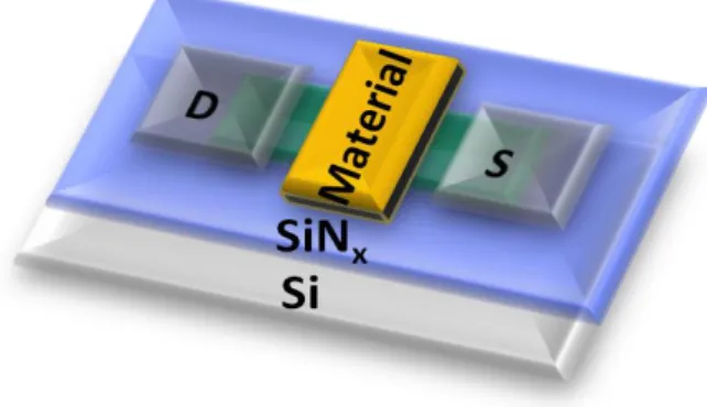
According to our early investigated in RF sputtering a-IGZO TFTs (Fig. 1-3),
material- capped in modifying back channel of a-IGZO TFTs could adjust the
threshold voltage in both positive and negative directions with capping different
materials [29] (Fig. 1-4). That is because the different work function and induce the
band bending in IGZO band tail states. This indicates a back gate bias (VBG) is
contributed from the intrinsic built-in voltage between IGZO body and the materials.
The TFTs operate at enhancement mode (normal off) or depletion mode (normal on)
look the work function of materials.
1-6 Thesis outline
In chapter 1, we introduced the development and theorems of IGZO based
transistor. The film mechanisms of metal-oxide are introduced. The experiment setup,
instrument and extraction parameters will be introduced in chapter2. The conventional
metal-oxide thin-film transistors and materials-capped TFTs are shown in chapter 3.
7
FIGURES of CHAPTER 1
8
Fig. 1.2 TG-DSC curves of IGZO sol-gel solution [7].
Fig. 1.3 Conventional bottom gate metal-oxide thin-film transistor.
9
CHAPTER 2
EXPERIMENT SETUP
2-1 Experimental procedure
In this section, device structure and process flow of the sol-gel metal-oxide films
based on TFTs and materials-capped TFTs used SiNx as dielectric was illustrated.
Conventional bottom gate TFTs
2-1.1 Sample preparation (wafer)
As shown in Fig. 2.1, a 6-inch p-type heavily-doped silicon wafer was used as
substrate and gate electrode for fabricating top-contact bottom-gate TFTs.
1. Deposition of SiNx dielectric:
1000Å silicon nitride (SiNx) developed dielectric layer to fabricate metal-oxide
devices. The SiNx layer was deposited using low pressure chemical vapor deposition
(LPCVD) at 780℃ with gases of NH3 and SiH2Cl2.
2. Removed SiNx on backside:
The backside silicon nitride on the silicon wafer was etched by reactive ion
etching (RIE). Prior to etching SiNx, photo-resist FH-6400 was coated on the foreside
of silicon wafer for protection. To remove SiNx layer on the back electrode of subtract,
gases including Oxygen (O2) 5sccm and Tetrafluoromethane (CF4) 80sccm were
10
respectively. After the RIE process, photo resist FH-6400 on the foreside of silicon
wafer was removed by using Acetone. After, the SiNx/wafer clean process including
SC1 and SC2 was required.
3. Cleaned the substrate:
Before started the experiment, the SiNx must be cleaned. Added acetone,
isopropanol in ultrasonic 10 to 20 minutes, then we used amount of DI water to
remove leftover solution, and dried by N2 air and baked on hot-plate to assure the
sample hold drying.
4. Metal-oxide thin-film formatted
The methods of producing metal-oxide sol-gel precursors were described at 2-2.
In order to assure the metal-oxide films uniform, the sample placed in UV-ozone for 5
to 10 minutes. Solution was spin-coated onto substrate for 1 to 3 times at a speed of
3,000 rpm for 30s and pre-heated at 200 ℃hotplate in the air for 3 min after each film
coating.
5. Post-annealing:
We used anneal furnace to anneal our sample. The annealing temperature was
200℃, 300℃, 400℃ and 600℃. The annealing time started from room temperature
to the temperature 10 min and lasted for 1h. Then the sample was placed in furnace
11
6. Wet-etching for metal-oxide films:
Put the sample on 170℃ hotplate for least 5 minutes, and put the stick negative
PR onto sample. Next step was using UV lithography through defined shadow mask
for 32 seconds (3W). Immersed the sample in preparing K2CO3 into DI water (the
percentage for K2CO3:DI water = 20mg:1ml) for 50 to 60 seconds, then washed the
remaining negative PR by DI water. We must remove the residue PR by using develop
solution , and then etching by dilute HCl(aq) (the dilute percentage for HCl(aq) :DI
water =1:4) solution with 100℃ for 4 to 10 seconds. Finally, put the sample on 120℃
hotplate for 10 minutes, remove PR by tweezers. Finally the active layer would be
defined.
7. Deposited Source and Drain electrode
Source and Drain electrode was deposited as Fig. 2.1. The metal materials of Al
were always used as Source and Drain electrodes on the metal-oxide TFTs. A
1000Å -thick Al film was deposited by using thermal coater and the rate of depositing
Al was 2.5Å /s. The electrodes were patterned by shadow mask. The channel length
varied from 200μm to 700μm and width was hold at 1000μm, respectively.
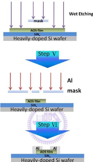
Materials-capped
metal-oxidetransistors
2-1.2
Materials-capped
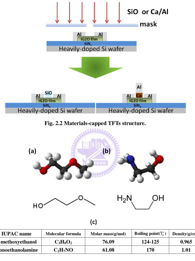
(SiO, Calcium)12
STD device as Fig. 2.2. In this case we used IGZO as metal-oxide film. A
thick-1000Å SiO-capped was deposited by thermal coater and the rate of depositing
SiO was 0.2 to 0.5Å /s. The SiO film was patterned by shadow mask and the capping
length was 100μm, 300μm, 500μm with the width/length was 1000μm/300μm, 1000μm/500μm and 1000μm/700μm, respectively. For Ca/Al film, 350Å Calcium was deposited with rate of 0.3 Å /s and 1000 Å Al was deposited to avoid Calcium
oxidation.
2-2 Fabricated of sol-gel
metal-oxideprecursors
In this section, ZnO, GZO, IGZO precursors would be described at 2-2.1, 2-2.3,
2-2.3. In our sol-gel metal-oxide precursors used 2-methoxyethanol (2-MOE) as a
solvent, mono-ethanolamine (MEA) as a stabilizer. Zinc acetate dehydrate
(Zn(OAc)2‧2H2O), gallium nitrate hydrate [Ga(NO3) 3‧xH2O] and Indium nitrate
hydrate [In(NO3) 3‧xH2O] powder used as Zinc, Gallium and Indium precursors.
MEA could help the hydrolysis in precursors. When high temperature treated, the
stabilizer were be evaporated and into air atmosphere.
2-2.1 ZnO precursors
The zinc-oxide precursor solution was first mixed 2-MOE and MEA. After
stirring for 10 min, (Zn(OAc) 2‧2H2O) added to the solution. The solution continued
13
last prescription for us was 2-MOE 10ml, MEA 0.28g, (Zn(OAc)2‧2H2O) 1g . We
adjusted the stirring atmosphere in glove box, stirred normal and vigorously in air and
stirred in high temperature (60℃).
2-2.2 GZO precursors
The method was similar to ZnO precursor, after adding (Zn(OAc)2‧2H2O),
dissolving amount of Gallium with a doped ratios of 0 at%, 1 at% and 5 at% with
Zinc acetate into solvent.
2-2.3 IGZO precursors
After adding zinc precursor into solvent, [Ga(NO3) 3‧xH2O] and [In(NO3)
3‧xH2O] were dissolved into to the solution. The best prescription presently was
2-MOE 1ml, MEA 2.52g, (Zn(OAc)2‧2H2O) 1g, [Ga(NO3) 3‧xH2O] 1.165g,
[In(NO3) 3‧xH2O] 0.890g, The molar ratio for Indium : Gallium : Zinc (In:Ga:Zn)
was 1:2:2 (atomic ratio).
2-3 Operation mechanism and parameter of transistors
2-3.1 Operation mechanism
The sol-gel ZnO, GZO and IGZO TFTs are n-type materials and voltage applied
to form a channel (although the doping will result the devices are operated at
depletion mode or enhancement mode). The channel is where delocalized electrons
14
the gate electrode. As the channel was formed, a voltage applied to the drain electrode
of the TFTs, these delocalized electrons in the accumulation layer are extracted from
the channel, giving rise to drain current path through the TFTs. The later section we
will report the definition of linear region and saturation region and their current
function.
2-3.2 Linear regions
Since the metal-oxide semiconductor films in our experiment is an n-type
materials, as a small drain voltages, i.e., voltages smaller than the gate voltage minus
the threshold voltage, VDS<VGS-VT, the linear region equation could be applied to
metal-oxide TFTs and could be expressed as
μ ..………Linear region
where the threshold voltage(VT) is the voltage at which the intercept point of the
square-root of drain current versus voltage when the device operate in saturation
mode, COX is the insulator capacitance, μ is the linear mobility of the electrons, W is the width of the channel, L is the length of the channel. VGS and VDS are the
gate-to-source and drain-to-source voltage, respectively.
2-3.3 Saturation regions
As the drain voltage reaches the pinch-off voltage, i.e., the voltage at the channel
15
is given by
μ ……….……….………Saturate region
2-3.4 Mobility
The field effect mobility (μFE) is determined by the orientation of active layer molecules near gate dielectric. Therefore, gate dielectric surface states strongly affect
the device μFE. μFE can be extracted to the linear mobility or saturation mobility. A large mobility value means that the device can conduct more current. Generally,
mobility can be extracted from the transconductance maximum gm in linear region:
μ
………Linear region The field effect mobility in the linear region could be extracted from the
transconductance and this equation can be expressed as
μ
………....………Linear region
The saturation mobility is another commonly used type of mobility. It is extracted
from an ID-VG curve when the device is biased in saturation, and could be extracted
from the transconductance and this equation can be expressed as:
μ ………..….………Saturate region Then: μ ………Saturate region
16
2-4 Experimental instruments
2-4.1. Spin coater
Spin coated process is suitable especially for dissolvent materials. The active
layer can be fabricated by spin coating. The initial spin speed determined the
thickness of thin film, and the final spin speed determined the uniformity of the film.
After spinning, the pre-heat process is proceeded to evaporate the solvent of the
solution quickly and let the process active thoroughly.
2-4.2. Thermal evaporation
Material like aluminum (Al), silicon oxide (SiOx) is deposited as the contact
layer by using thermal evaporation. The thermal evaporation deposition technique
consists of heating the metal to evaporate and deposit on the cold substrate. The
process pressure was controlled about 5×10⁻⁶ torr to avoid the vapor to react with
atmosphere. The average energy of the vapor atoms reaching to the substrate surface
is about 10 eV.
2-4.3. Four-point probe resistivity measurement
The four-pint probe configuration is usually used to measure the sheet resistance
of a semiconductor. Four identical probes are placed in a linear configuration, equally
spaced, along the sample. Current is forced through the outer probes, while the
17
impedance meter, which minimizes the current flow, thereby minimizing the contact
resistance to a negligible value.
2-4.4. Atomic force microscope measurement
Since we expect ZnO film are different from IGZO and GZO film, atomic force
microscope (AFM) is used to measure surface morphology on a scale from angstroms
to 30 microns. It scans samples through a probe or tip, with radius about 20 nm. The
tip is held several nanometers above the surface and using feedback mechanism that
measure interactions between tip and surface on the scale of nanometers. Variations in
tip height are recorded when the tip is scanned repeatedly across the sample, then
producing morphology image of the surface. In this experiment, the used equipment is
Digital Instruments D3100 as shown in Fig. 2-3 and the used active mode is tapping
18
19
20
Fig. 2.2 Materials-capped TFTs structure.
IUPAC name Molecular formula Molar mass(g/mol) Boiling point(℃) Density(g/cm3) 2-methoxyethanol C3H8O2 76.09 124-125 0.965
monoethanolamine C2H7NO 61.08 170 1.01
Fig. 2.3 Chemical structures of the (a) 2-methoyxethanol (b) monoethanolamine (c) the chemical properties.
21
CHAPTER 3
RESULT and DISCUSSION
3-1 The leakage of solution-processed metal-oxide TFTs
In our experiment, a 100-nm-thick layer of thermal silicon nitride (SiNx) was
grown onto silicon wafers to serve as the dielectric and the capacitance was
5.31×10-08 F/cm2. To avoid producing a large current, the metal-oxide films were
isolated by a wet etching process with dilute hydrochloric acid (HCl(aq): DIW=1:5). If
the active layer were not isolated, the leakage current path from drain electrode or
source electrode to gate electrode by the whole active layer result a large leakage
current and ruin the TFTs device. In the ideal condition, ID+IS+IG=0. Decrease the
gate leakage would induce the origin of drain current or source current.
Fig. 3.1 showed the transfer characteristics of the zinc-oxide TFT at a drain-source
voltage VDS of 40V, the annealing temperate was 600℃, exhibiting a typical
n-channel enhancement field-effect behavior. It clear sees that the IG current in black
dash line is larger than the red dash line. And the IG current maintained at 10-9(A)
even in large gate voltage. The sub-threshold swing, S.S, decreased from
5.54(V/decade) to 0.64(V/decade), without wet etching and after wet etching,
respectively. The good performance for pattern TFTs avoided large leakage currents
22
3-2 Bottom gate top contact zinc-oxide TFTs
Metal-oxide is a flexible material with easily tunable phases that can crystal to
amorphous or crystallization. Oxygen vacancy is an accepted electron donor in metal
-oxide film. Therefore, the oxygen quantity significantly influences the conductivity
or carrier concentration in metal oxide. As regard to the application on
semi-conductive metal-oxide, the oxygen ratio controlling seems critical and
important. In solution processed metal-oxide TFTs, There are some experiment
parameters to controlled oxygen ratio, such as adjusted the process atmosphere (N2,
O2), adjusted the process annealing temperature and adjusted the precursor solutions.
A set of experiment parameters could determine the final oxygen ratio or carrier
concentration in metal-oxide films. In our study, in order to get the best performance
of TFTs, we tested above methods and process conventional TFTs. This study was
expected to provide a useful guideline to do other device structure.
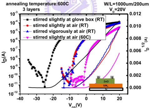
3-2.1 Zinc-oxide TFTs characteristics in different precursor solution stirred atmosphere
In order to get high mobility, low sub-threshold swing and near zero threshold
voltage TFT, we adjusted different precursor solutions atmosphere to fabricate ideal
metal-oxide film. In the section, the annealing temperature for zinc-oxide 3-layers
was hold at 600℃. From the beginning, we produced colorless, clear solutions with
23
The negative threshold voltage, beyond we expect (See in Fig. 3.2 and Table 3-1).
Y. S. et al. reported that the precursor solution stirred in air would enhance the IPCE
of organic solar cell. [30] We tested this method for further investigation. In
fabricating the zinc-oxide precursor (the concentration for precursor solution was
0.43M), we placed the precursor onto the hot-stirring (stirred rate was 250rpm/s) in
air atmosphere at room temperature for 12 h for the hydrolysis reaction in air. The Voff
and VT we estimated at this moment was slightly positive shift than early, moved to
-2.15V. When zinc-oxide precursor solution stirred rate raise to 400rpm/s, the
threshold voltage moved unobvious. Saturation mobility from 1.76 cm2V-1s-1 slight
increased to 2.24 cm2V-1s-1, and VT positive shifted so slightly that we did not find
almost. We raise the film annealing temperature up to 60℃ (placed in hot-stirring
with 250rpm/s and 60℃), the mobility decreased slightly, but the VT and Voff became
more positive, even though the on current, on/off ratio, was small than the devices we
produced than before, but the positive threshold voltage seemed important to further
work. The negative VT in such case no matter zinc-oxide thin-film transistor and
indium-gallium-zinc-oxide thin-film transistor may be observed, there might have
some mechanism in it. We considered that there was one or all of following reasons.
First, when the solutions were stirred at high temperature in air atmosphere, the
24
would thicker than we expected. Second, stirring at high temperature might result the
change of metal-oxide precursors. In order to realize that first reason was right or
wrong, we designed to vary different active layers to make the zinc-oxide TFTs. From
Fig. 3.3, the thicker thickness may result the more negative VT. This result told us
evaporating of solvent could not induce the threshold voltage shifted to positive. The
phenomenon for negative threshold voltage shift was conjectured because when the
thickness of zinc-oxide film increased, we must need more negative voltage to
suppress the TFT. [10] Contrary to the thickness of metal-oxide film, the primarily
cause for negative shift of zinc-oxide precursor solution stirred in glove box is
because the different ratio for oxygen vacancies. Since the precursor stirred in glove
box was at a atmosphere of lock of O2, the lock of O2 induced the incomplete of
precursor and result the conducted was lead by metal ion stacking in metal-oxide film,
the performance of TFTs was because of rising a larger number of oxygen vacancies
and zinc interstitials. The precursor solutions stirred in air atmosphere or at high
stirred temperature seemed increased the rate of hydrolysis of zinc-oxide precursor
complete so that we only need small gate voltage, the TFT devices turn on quickly.
Besides, the highest mobility we extracted was
2.24 cm2V-1s-1 (the precursor solution stirred vigorously in air at room temperature)
25
We observed similar result in AFM (see Fig. 3.4). When the zinc-oxide precursor
solution stirred in air at 60℃, the roughness for zinc-oxide film seem different from
zinc-oxide precursor solution stirred at room temperature. The large crystal for
zinc-oxide film supported our hypothesis so that we could adjust the precursor
solution atmosphere to control the threshold voltage we want.
3-3 Bottom gate top contact gallium-zinc-oxide TFTs
Although zinc-oxide TFTs exhibited high on/off ratio, high mobility (~2.24
cm2V-1s-1) at high annealing temperature, but the zinc-oxide TFT had a poor
performance in lower annealing temperature, result we find other new metal-oxide
film to replace zinc-oxide film. The spin-coated 3 layers gallium-zinc-oxide films
were prepared on the SiNx gate insulator layer at 600 °C to investigate electrical
properties. Fig. 3.5 and Table 3-2 showed the Transfer ID-VG curves and parameters of
the gallium-zinc-oxide TFTs. In early study [17], we had known the drain-to-source
current and mobility of the gallium-zinc-oxide TFTs would lower than zinc-oxide
TFTs. But the threshold voltage of gallium-zinc-oxide TFT negative shifted beyond
our expected. In the W. J. Park et al. research [6], the Hall mobility and carrier
concentration would increase with increase Gallium doping, and then get a maximum,
finally decreased with increasing Gallium atom ratio. This was because when carrier
26
speaking, less conductance showed positive threshold because more interface trap
density. High trap density caused a larger threshold voltage since more voltage was
required to fill in. The VT of the 5 at% gallium-zinc-oxide TFT (-27,10V) was more
positive than 1at% GZO TFT (-24.95V), we conjectured that the carrier concentration
for 5at% GZO TFT was lower than 1 at% GZO TFT. But after all, the negative shifts
of the GZO TFTs were not we want.
3-4 Bottom gate top contact indium-gallium-zinc-oxide TFTs
Since the annealing temperate and the carrier concentration limited developing of
the zinc-oxide and gallium-zinc-oxide TFTs, indium-gallium-zinc-oxide film effect
transistor, was regarded as a new doping metal-oxide film compare to above
metal-oxide TFT. It had studied that adjusting composition of indium, gallium and
zinc molar ratio could get different performance of TFTs [6], [10], [31]. In our
devices, The mole ratio of In:Zn was fixed as 1:2 and In:Ga was varied from 1:1 to
1:2 (i.e., the following mole ratios were prepared by In:Ga:Zn = 1:1:2 and 1:2:2).
Similar to 3-2.1, we wanted to produce high mobility, positive sub-threshold voltage
(VT>0) in low annealing temperature. In this section, we would discuss the different
annealing temperature of the indium-gallium-zinc-oxide TFTs, different precursor
stirred atmosphere and the different doped ratio of the indium-gallium-zinc-oxide
27
3-4.1 The precursor solutions in different stirring atmosphere
3 layers of indium-gallium-zinc-oxide films were spin-coated onto the SiNx
substrate at 600 °C annealing temperature to investigate the device electrical
properties. Fig. 3.6 and Table 3-3 are ID-VG curve and parameters of the
indium-gallium-zinc-oxide thin-film transistors with different molar ratio and the
different stirring temperature. From Fig. 3.6, we observed similar result contrary to
zinc-oxide thin-film transistors (see chapter 3-2.1). When the precursor solutions were
stirred at room temperature, the VT for IGZO (1:1:2) and IGZO (1:2:2) were -10.78V
and -2.24V, respectively. But when the solutions were stirred at 70℃, the VT all
positive shift from -8.74V (1:1:2) to 3.73V (1:2:2), respectively. the more negative VT
for IGZO(1:1:2) had been discussed in early paper[6], that was because the structure
of indium-gallium-zinc-oxide consists of alternate stacking of InO2- layers and
GaO(ZnO)m+ blocks. Increased Gallium doping ratio would reduce the doped
sensitivity to the O2 partial pressure. Since the bonding of O-Ga-O larger than Zn-O
and In-O bonding, Gallium doping increased would result the decreased in oxygen
vacancies and decrease in mobility, in other words, Gallium content doping would
decrease the electro-negativity and carrier concentration, resulting the positive shift in
VT in order to fill in the prefilled of trap states in compensate the lock of oxygen
28
structure, (different in GaO(ZnO)m+, wurtzite structure). So the solubility of In3+ was
limited and the insoluble of InO2- could result in the cubic stacking faults in the IGZO
layer and layer. Increasing the In molar ratio would let the stacking layer of InO2
-more than we expected and enhance the metal character, resulting the VT negative
shift when increasing the In molar ratio, that was why the device of the
In:Ga:Zn=3:1:2 thin-film transistor we produced couldn’t turn off at the quite
negative gate-to-source voltage and the drain current was still on(the data was not
shown in here).
3-4.2 The different annealing temperature for IGZO (1:2:2) TFTs
Fig. 3-7, Fig. 3-8 and Table 3-4 showed when decreased the post-annealing
temperature, the decreased in mobility and on/off ratio. We hoped to produce the
thin-film transistors with low temperature during post-annealing. The oxide-lattice
formation and oxygen-vacancy generation depends primarily from the annealing
temperature. Although the mobility in low temperature seemed crucial, we still
observed the characteristics of thin-film transistors. The mobility(~10-4cm2V-1s-1)
and negative VT (-51.64V) for 200℃ Thin-film transistor limited the application of
indium-gallium-zinc-oxide, but contrast to the low post-annealing temperature
devices, the high annealing temperature limited the choose of insulator and electrode.
29
used 400℃ and 600℃ annealing temperature to continue the later experiment.
3-4.3 The influence of stabilizer in indium-gallium-zinc-oxide TFT
In the above experiment, we used the same stabilizer contrary to zinc-oxide
precursor solution to do our indium-gallium-zinc-oxide device test. But for
indium-gallium-zinc-oxide case, the film seem so rough that the contacts for
indium-gallium-zinc-oxide and electrode or dielectric are poor (Fig. 3-9). The
roughness for indium-gallium-zinc-oxide film was 18.55nm and beyond our expected.
We want to get smooth surface in indium-gallium-zinc-oxide film and applied to
SCLT (space-charge-limited transistors) in future, so we want to solve the problem.
Some paper had reported [31] that adding more stabilizers into the precursor solution
to form a uniform sol-gel solution. The molar ratio of ethanolamine to indium,
gallium and zinc was maintained as 5:1, 1:1, and 1:1, respectively. We used the
prescription to form indium-gallium-zinc-oxide film and found that the roughness for
indium-gallium-zinc-oxide film decreased to 0.52nm. Then we used the new
indium-gallium-zinc-oxide film to make TFT and find that the mobility had enhanced
to ~2cm2V-1s-1 (Fig. 3-10). The large enhance in mobility we guessed that was the
solubility limit in indium precursor powder that we must added more stabilizer to let
indium pre-reaction to form a gel. If not enough stabilizer added, the precursor did not
30
in AFM. The smooth indium-gallium-zinc-oxide film could let us replace zinc-oxide
film to form a pore film structure, and did not damage the device.
3-5 The standard thin-film transistor with materials-capped
In the early investigate of sputter indium-gallium-zinc-oxide Thin-film transistor
[29], capping some materials onto standard thin-film transistor could adjust the
threshold voltage, enhanced the drain current and result raising the mobility of
devices. The physical hypothesis of enhancing drain current and mobility must be
check in further investigate, but it give a way to get high performance in low
annealing temperature.
3-5.1 SiO-capped onto standard indium-gallium-zinc-oxide thin-film transistor
The standard solution-processed indium-gallium-zinc-oxide TFTs with different
channel length showed in Fig. 3-11 and Table 3-5, and Fig. 3-1, Fig.3-12, Table 3-6
presented the transfer characteristics of SiO-capped indium-gallium-zinc-oxide
thin-film transistors with different percentage of capping layer. In this time we
defined a new parameter, capping ratio. And
. During
device operation, the materials were floated and no bias voltage across it. The
materials-capped layer for SiO did not form a current leakage path from source
31
did not change obviously but the mobility increased from 2.32 cm2V-1s-1, 2.60
cm2V-1s-1 and 2.11 cm2V-1s-1 to 3.31 cm2V-1s-1, 10.2 cm2V-1s-1 and 15.2 cm2V-1s-1 with
increasing the capping ratio, respectively. The enhanced in mobility because increased
the drain current. Besides, all these materials-capped devices possessed a compared
sub-threshold swing (0.31–0.47 V/decade) and threshold voltage(-0.48–0.11V). We
considered the enhance mobility of the devices because the capping of SiO layer
would grab the oxygen in the interface of indium-gallium-zinc-oxide, and result the
oxygen vacancies increased on the back surface. Since , the
oxygen vacancies will produce two free electrons and there are a gradient of electrons
in the back surface. The high carrier concentrations of free electrons will decrease the
series resistance on back surface, and there are more pathways for electrons to across
from source electrode to drain electrode. The drain current increased from 10-5 to 10-4
(A) in gate voltage at 20V, and with the increase of capping ratio, the saturation
mobility increased more obvious. Besides, the sub-threshold swing and on/off ratio(~
106) did not change a lot. This revealed the good characteristics of capping SiO
indium-gallium-zinc-oxide thin-film transistor.
In order to get high mobility at low annealing temperature (about~1 cm2V-1s-1),
we decreased the annealing temperature (400℃) to produce standard and
32
Table 3-8). The IGZO (1:2:2) TFT mobility was so slightly (different in the early we
mentioned); we guessed the instable in low annealing temperature and result the
breakdown of increasing mobility. Since the oxygen vacancies increased because the
grabbing of oxygen in capping SiO, when the devices placed in the air atmosphere
long time, the oxygen in air would fill the oxygen vacancies in the back surface and
result the decreasing of oxygen vacancies.
Contrast to IGZO (1:2:2) TFTs, IGZO (1:1:2) TFTs showed large enhance in
mobility in the low annealing temperature (400℃) (Fig. 3.15 and Table 3-8). The
mobility enhanced from~0.1 cm2V-1s-1 to ~1 cm2V-1s-1. This result let us find some
ways to produce low temperate IGZO TFTs with high performance.
3-5.2 Calcium-capped onto standard indium-gallium-zinc-oxide thin-film transistor
Fig. 3.16 showed the ID-VG curve for capping and uncapping devices with
different channel lengths (i.e. the capping ratio were 3/5 and 5/7, respectively). The
composition of indium-gallium-zinc-oxide was 1:1:2 and the annealing temperature
for indium-gallium-zinc-oxide were at high temperature (600℃). There are significant
VT negative shifts whether the increase in capping ratio. The slopes of ID-VG curves
were raised by metallic capping layers, indicating a significantly improved field
33
lists the extracted typical parameters of IGZO (1:1:2) TFTs. The △ VT is the threshold
voltage difference between standard and Calcium-capped devices. The △ VT is
-9.96V, -8.74V with different capping ratio, respectively. The hypothesis of the
enhancing mobility and VT shift had been demonstrated from the sputter a-IGZO
TFTs [29]. Fig. 3-18 was the band diagram of indium-gallium-zinc-oxide and
Calcium. After contact with Calcium, The injected electrons accumulate near the
interface between indium-gallium-zinc-oxide and Calcium to form a channel. The
system could be regarded as a conventional dual Gate TFT that has a control gate with
a positive gate-to source voltage (normal on). The voltage is contributed from the
work function difference, . Because Calcium generated a channel on the indium-gallium-zinc-oxide back surface, the VT became more negative to suppress
the initially existed channel to turn-off the device depletion mode TFT. The electrons
injected on the interface between the indium-gallium-zinc-oxide film and dual gate
(Ca) and formed a channel. The high conductance channel provided a pathway of
electron transmit. This result enhanced the drain-to-source current, about one order.
And the mobility improved with the slope of -VG, from 1.28 cm2V-1s-1 to 13.2
cm2V-1s-1 (capping ratio was 3/5) and 1.17 cm2V-1s-1 to 13.7 cm2V-1s-1 (capping ratio
34
FIGURE of CHAPTER 3
-40 -20 0 20 40 10-12 10-11 10-10 10-9 10-8 10-7 10-6 10-5 10-4 10-3 3 layers annealing temperature:600C VD=40V W/L=1000um/200um I G (A ) I D (A ) V (V)ID, before wet etching ID, after wet etching
10-12 10-11 10-10 10-9 10-8 10-7 10-6 10-5 10-4 10-3
IG, before wet etching IG, after wet etching
Fig. 3.1 The ID-VG curve of the ZnO TFTs with and without wet etching
(the annealing temperature at 600℃)
-40 -30 -20 -10 0 10 20 10-12 10-11 10-10 10-9 10-8 10-7 10-6 10-5 10-4 10-3 Si SiNx ZnO D S 3 layers W/L=1000um/200umVD=20V annealing temperature:600C I D 1 /2 (A ) I D (A ) VGS(V)
stirred slightly at glove box (RT) stirred slightly at air (RT)
stirred vigorously at air (RT) stirred slightly at air (60C)
0.000 0.002 0.004 0.006 0.008 0.010 0.012
Fig. 3.2 The ID-VG curve and -VG characteristics of the ZnO TFTs by
adjusting precursor solution in different atmosphere. (The channel width /channel length, W/L=1000μm /200μm)
35
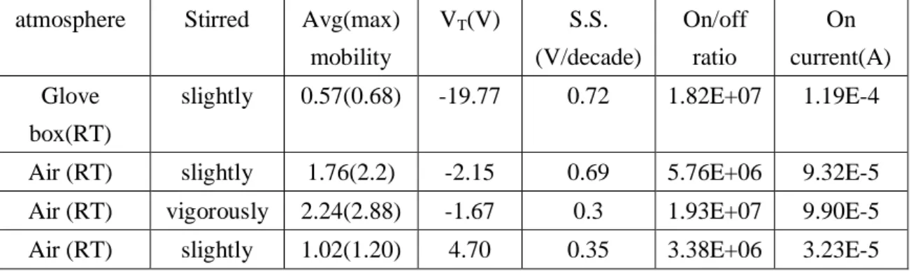
atmosphere Stirred Avg(max) mobility VT(V) S.S. (V/decade) On/off ratio On current(A) Glove box(RT)
slightly 0.57(0.68) -19.77 0.72 1.82E+07 1.19E-4
Air (RT) slightly 1.76(2.2) -2.15 0.69 5.76E+06 9.32E-5 Air (RT) vigorously 2.24(2.88) -1.67 0.3 1.93E+07 9.90E-5 Air (RT) slightly 1.02(1.20) 4.70 0.35 3.38E+06 3.23E-5 Table 3-1 the parameters for ZnO TFTs by adjusting precursor solution in
different atmosphere.(The ZnO film annealed at 600℃) (The channel width /channel length, W/L=1000μm /200μm)
-35 -30 -25 -20 -15 -10 -5 0 5 10 15 20 25 10-10 10-9 10-8 10-7 10-6 10-5 10-4 Si SiNx ZnO D S VD=20V ZnO TFT 600C 1 hr I D (A ) VGS(V) 1 layer (40nm) 3 layers (80nm) 5 layers (130nm) 0.000 0.002 0.004 0.006 0.008 0.010 0.012 0.014 0.016 I D 1 /2 (A ) v
Fig. 3.3 The ID-VG curve and -VG characteristics for different channel
layers of the ZnO TFTs.(The precursor solution was stirred in glove box at RT)(The channel width /channel length, W/L=1000μm /200μm)
36
Fig. 3.4 AFM images of different precursor solutions stirring atmosphere (a)stirred slightly (b)stirred vigorously (c) stirred slightly at 60℃.
-40 -30 -20 -10 0 10 20 10-9 10-8 10-7 10-6 10-5 10-4 10-3 Si SiNx GZO D S VD=20V GZO TFT annealing temperature:600C I D (A ) VGS(V) GZO(1at%) GZO(5at%) 0.000 0.005 0.010 0.015 0.020 0.025 I D 1 /2 (A )
Fig. 3-5 The ID-VG curve of the GZO TFTs according to different
Ga-incorporated solutions. (the solution stirred in air at RT) (The channel width /channel length, W/L=1000μm /200μm) Annealing temperature Ga doped ratio Avg(max) mobility(cm2/V.s) VT(V) S.S. (V/decade) On/off ratio On current(A) 600℃ 1at% 1.94(1.95) -27.10 1.84 2.96E+05 5.84E-4 600℃ 5at% 1.10(1.15) -24.95 1.45 1.43E+05 1.61E-4
Table 3-2 the parameters for GZO TFTs according to different Ga-incorporated solutions. (Solution was stirred in air at RT)
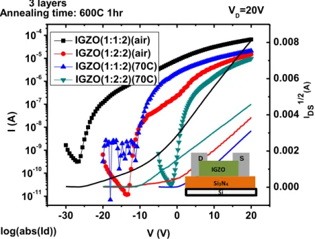
37 -30 -20 -10 0 10 20 10-11 10-10 10-9 10-8 10-7 10-6 10-5 10-4 I (A ) V (V) IGZO(1:1:2)(air) IGZO(1:2:2)(air) IGZO(1:1:2)(70C) IGZO(1:2:2)(70C) 0.000 0.002 0.004 0.006 0.008 Si Si3N4 IGZO D S VD=20V 3 layers I DS 1 /2 (A ) log(abs(Id)) Annealing time: 600C 1hr
Fig. 3.6 The ID-VG curve and -VG characteristics for different mixed
ratio (1:1:2 and 1:2:2) of the IGZO TFTs in different precursor condition. (The channel width /channel length, W/L=1000μm/200μm)
Stirred temperature In:Ga:Zn Avg(max) mobility(cm2/V.s) VT(V) S.S. (V/decade) On/off ratio On current(A) RT 1:1:2 0.91(1.15) -10.78 1.31 2.07E+05 6.57E-5 RT 1:2:2 0.80(0.89) -2.24 0.57 1.29E+06 1.49E-5 70℃ 1:1:2 0.43 (0.57) -8.74 0.16 3.00E+06 2.10E-5 70℃ 1:2:2 0.58 (0.76) 3.73 0.77 3.16E+05 9.71E-6 Table 3-3 the parameters for IGZO thin-film transistors in different mixed
ratio and different precursor condition.
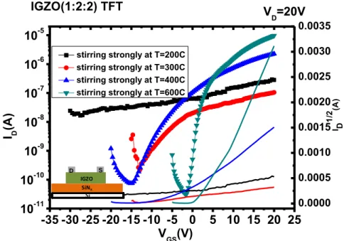
38 -35 -30 -25 -20 -15 -10 -5 0 5 10 15 20 25 10-11 10-10 10-9 10-8 10-7 10-6 10-5 Si SiNx IGZO D S VD=20V IGZO(1:2:2) TFT I D (A ) VGS(V) stirring strongly at T=200C stirring strongly at T=300C stirring strongly at T=400C stirring strongly at T=600C 0.0000 0.0005 0.0010 0.0015 0.0020 0.0025 0.0030 0.0035 I D 1 /2 (A )
Fig. 3.7 The ID-VG curve and -VG characteristics for IGZO(1:2:2)
thin-film transistors(The channel width /channel length, W/L=1000μm/200μm) annealing temperature Avg(max) mobility(cm2/V.s) VT(V) S.S. (V/decade) On/off ratio On current(A) 200℃ 3.5E-04(4.3E-04) -51.64 4.75 1.78E+01 2.81E-7 300℃ 7.8E-03(6.3E-03) -15.30 1.66 4.83E+02 1.04E-7 400℃ 0.048 (0.16) -12.27 2.93 3.05E+04 2.27E-6 600℃ 0.58 (0.76) 3.73 0.77 3.16E+05 9.71E-6
Table 3-4 The annealing temperature with IGZO(1:2:2) thin-film transistors(The channel width /channel length, W/L=1000μm/200μm)
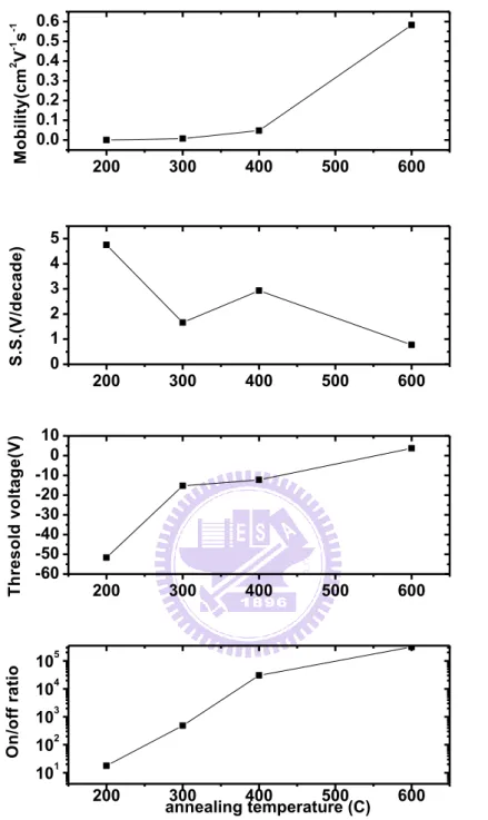
39 200 300 400 500 600 0.0 0.1 0.2 0.3 0.4 0.5 0.6 M o b il it y (cm 2 V -1 s -1 200 300 400 500 600 0 1 2 3 4 5 S .S .( V /d e c a d e ) 200 300 400 500 600 -60 -50 -40 -30 -20 -10 0 10 T h re s o ld v o lt a g e (V ) 200 300 400 500 600 101 102 103 104 105 O n /o ff r a ti o annealing temperature (C)
Fig. 3.8 The evolution of electric parameters (a) Mobility, (b) VT (c) S.S. (d)
40
Fig. 3.9 AFM images of different stabilizer in IGZO precursor solution. (a)Few stabilizer (b)more stabilizer.
-5 0 5 10 15 20 10-12 10-11 10-10 10-9 10-8 10-7 10-6 10-5 10-4 VD=20V Annealing temperature=600C I D 1 /2 (A ) I D (A ) VGS(V) Few stabilizer More Stabilizer 0.000 0.002 0.004 0.006 0.008 0.010
Fig. 3.10 The ID-VG curve and -VG characteristics for IGZO(1:2:2)
![Fig. 1.1 The carrier transport paths in covalent semiconductors and AOS [12].](https://thumb-ap.123doks.com/thumbv2/9libinfo/8043310.162002/23.892.138.758.237.772/fig-carrier-transport-paths-covalent-semiconductors-aos.webp)