A CMOS transmitter front-end with digital power control for
WiMAX 802.16e applications
Yu-Hsuan Liu, Hsiao-Chin Chen, Tao Wang and Shey-Shi Lu
Graduate Institute of Electronics Engineering, National Taiwan UniversityAbstract: A 5.8 GHz transmitter front-end comprising a quadrature modulator, a variable gain
amplifier and an on-chip output balun in CMOS 0.18-um technology is presented. The quadrature modulator adopts cross-coupled type micro-mixer, and the measured 3rd-oder rejection is 32 dB under
input voltage swing of 250 mVpp. With four-bit control words, a 16-step linear-in-dB output power is realized to achieve a dynamic range of 27 dB. A single-ended type output is accomplished by an on-chip 3:1 transformer and the output matching network is therefore simplified.
Key Words: RF, transmitter, VGA, digital control, linear-in-dB I. INTRODUCTION
Recently, the IEEE has come up with a new standard, 802.16e, also known as WiMAX, which is a short name for World Interoperability for Micro-wave Access. WiMAX is a broadband wireless technology which promises not only high data-rates but also long connection distances. Standards and applications based on this attractive technology are scheduled for initial deployment in mid-to-late 2005. Since WiMAX adopts OFDM modulation scheme for high data-rates, the modulated signals will display a high Peak-to-Average Power Ratio (PAPR) and a strict linearity requirement in transmitter can be expected. Besides, 802.16e support a roam mode which provides each user a connection with cell phone quality, therefore, a wide output power range is necessary. In this paper, the design issues such as the linearity, the output power range, and the linear-in-dB gain control are considered and discussed. To facilitate the integration with off-chip power amplifiers in general purposes, an on-chip transformer of 3:1 turn-ratio is used to convert the differential output signal of the variable gain amplifier (VGA)to a single-ended signal.
II. CIRCUIT BLOCK
The architecture of the transmitter front-end is shown in Fig. 1. A quadrature modulator is followed by a VGA which contains an on-chip transformer of 3:1 turn-ratio. The base-band signal is up-converted by the modulator and then amplified by the two-stage VGA. Four digital bits are manipulated to control the gain of the VGA in a linear-in-dB fashion. The LO signal is applied externally through a rat-race hybrid, and converted into quadrature signals by a poly-phase filter.
Fig. 1 Transmitter Front-end Architecture
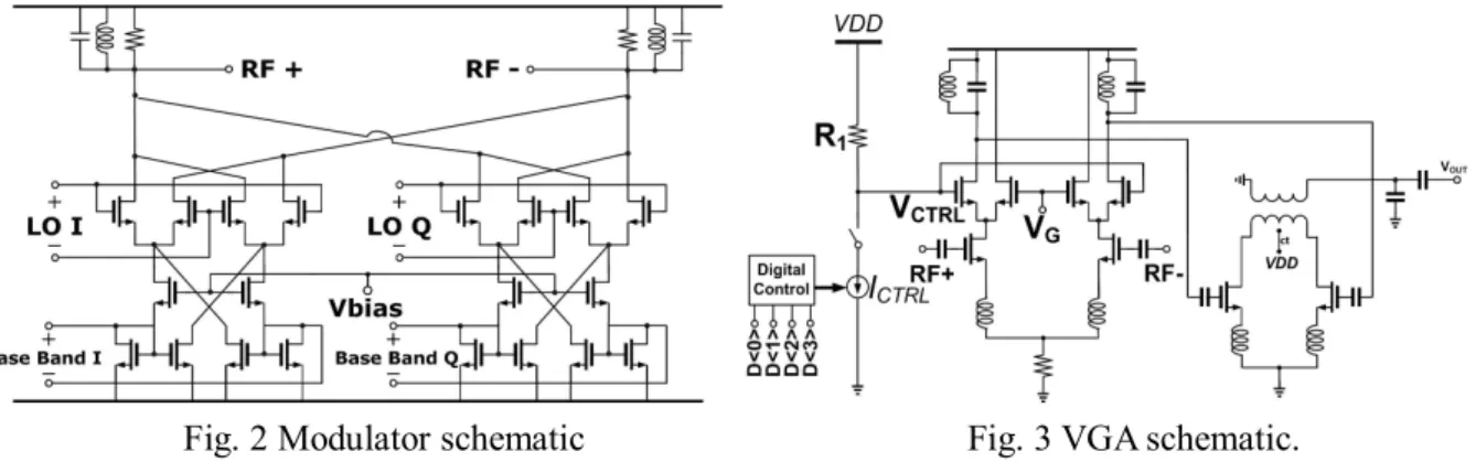
The schematic of the modulator is shown in Fig. 2. The modulator is based on the asymmetry class-AB topology of the MicroMixer [1] and the transconductance stage is cross-coupled to maintain the symmetry in base-band signals. With the class-AB structure, the modulator can handle larger base-band signals and provide a wider input dynamic range. With proper device selection, the nonlinear phenomenon respectively occurs in the common-gate and the common-source MOSFETs can be cancelled by each other under a particular bias condition [1].
Fig. 2 Modulator schematic Fig. 3 VGA schematic.
The gain control is realized with a current steering structure in the first stage of the VGA as shown in Fig.3. The on-chip transformer offers its primary coil as the load inductors of VGA’s second stage, thus accomplishes a differential-to-single-ended conversion. The transformer was simulated by momentum with its physical layout shown in Fig.4 [2].
Fig. 4 Physical layout and schematic symbol of the transformer
to simplify the impedance matching between the output stage and the 50-ohm.
16 gain steps are achieved by the digital-control block shown in Fig. 5. The decoder first translates the four digital bits into 18 control words fed to the digital-to-analog-converter (DAC), which is composed of seven binary weighted current sources with source-coupled-logic switches. The DAC can create an output current by which the control voltage VCTRL is adjusted. Degeneration resistors are
used to reduce the mismatches between the current sources and an irregular coding is also utilized to minimize the gain step error.
Fig. 5 The digital control block and the schematic of DAC.
III. SIMULATION AND MEASUREMENT RESULTS
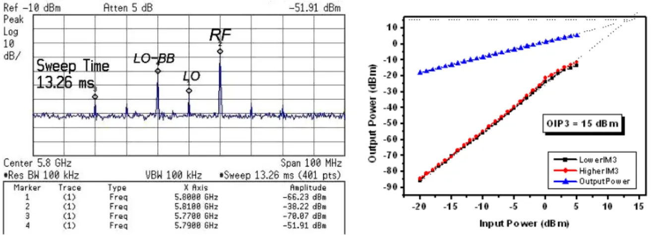
The transmitter front-end draws 53.3mA from a 2.8V supply. The quadrature base-band signals are applied by R&S AMIQ signal generator. The measured output spectrum of the modulator is shown in Fig. 6. The LO rejection is 28.0 dB, the sideband rejection is 13.7 dB, and the third order rejection is 31.9dB. The OIP3 of the VGA is about 15 dBm as shown in Fig. 7.
Fig. 6 Measured output spectrum of the modulator. Fig. 7 OIP3 measurement result. Fig. 8 shows the simulated dB-linear gain at each step. The linear-in-dB gain control characteristic is achieved with a 2.13-dB step and a ±0.8 dB gain error. The digital controllable range is over 33 dB. The measured dynamic range is about 27 dB as shown in Fig. 8. Although the gain range is smaller than the simulation result, it is wide enough for general applications.
Fig. 8 Simulated Gain versus input control words. Fig. 9 Dynamic range of VGA. The die photograph and evaluation board of the transmitter front-end are shown in Fig. 9 and Fig. 10, respectively. The total die area is 2.4mmx1.1mm.
Fig. 10 Die photograph of the transmitter front-end. Fig. 11 Evaluation board.
IV.CONCLUSIONS
A 5.8GHz CMOS transmitter front-end with digital linear-in-dB gain control is presented in this paper. The output signal demonstrates good performances in unwanted spur rejection and an OIP3 of about 15 dBm. This transmitter also has an output dynamic range of 27 dB.
V. ACKNOWLEDGMENT
Financial support from 91EC17A05-S10017, NSC 94-2215-E-002-032 and NSC
94-2218-E-002-045
is appreciated. The authors would like to thank CIC for chip fabrication and NDL for chip measurement.REFERENCES
[1] Barrie Gilbert, “The MICROMIXER: A Highly Linear Variant of the Gilbert Mixer Using a Bisymmetric Class-AB Input Stage,” IEEE J. SOLID-STATE CIRCUITS, vol. 32, no. 9, Sept. 1997 [2] Alessandro Italia, Egidio Ragonese, Luca La Paglia, and Giuseppe Palmisano, “A 5-GHz
High-Linear SiGe HBT Up-converter with On-chip Output Balun,” IEEE Radio Frequency