Measurement of Temperature Distribution in SnAg3.5 Flip-Chip
Solder Joints during Current Stressing Using Infrared Microscopy
Hsiang-Yao Hsiao, and Chih Chen
Department of Materials Science and Engineering, National Chiao Tung University, Hsin-chu 30010, Taiwan, Republic of China
281
Abstract
In this paper, the temperature distribution during electromigration in flip-chip SnAg3.5 solder bumps is directly examined using infrared microscopy. Two clear hot spots are observed in the bump. One is located at the region with peak current density, and the other one is at the bump edge under the current-feeding metallization on the chip side. Under a current stress of 1.06 x 10⁴A/cm2
, the temperature in the two
hot spots are 161.7 °C and 167.8 °C, respectively, which surpass the average bump temperature of 150.5 °C. In addition, effect of under-bump-metallization (UBM) thickness on the hot spots is also examined.Itindicates that the hot-spot temperature in the solder bump increases for the solder joints with a thinner UBM.
I. Introduction
Flip chip technology has been adopted for high-density packaging due to its excellent electrical performance and better heat dissipation ability.1As the required performance in microelectronic devices becomes higher, the current that each bump needs to carry is 0.2 A, and it will increase to 0.4 A in the near future. Furthermore, to meet the miniaturization trend of portable devices, the dimensions of the solder bumps continue to shrink, causing the current density in each solder joint to increase abruptly. Therefore, electromigration the solder bumps become an important issue?
Several investigations on electromigration in flip-chip solder joints have been carried OUt.3-1OCurrent crowding effect occurs seriously near the entrance point of the Al trace into the solder joint, which is responsible for the failure in the chip/anode side of the solder joint.4
-5 Furthermore, Joule
heating effect also takes place during accelerated electromigration tests.6-10 During electromigration tests, the
applied current may be as high as 2.2 A,3 which may cause serious Joule heating in the solder joints. The temperature increase due to current stressing may be over 30°C when a 1.0 A current is applied to the solder bump.5-7 In addition, several simulation studies point out that there exists a hot spot in the solder bump near the entrance of the Al trace.7-9On the other hand, Lai et al. show that there is no such hot spot based on their simulation results.11 The temperature may affect the mean-time-to-failure (MTTF) significantly, as depicted by Black's equation:12
MTTF
=
A_I
exp
(..!)
(1)jn
kT
where A is a constant, j is the current density in amperes per square centimeter, n is a model parameter for current density, Q is the activation energy, k is Boltzmann's constant, and T is
the average bump temperature in degrees Kelvin. However, no experimental results have been reported to confirm the existence of the hot spot. This is because the solder joints are completely surrounded by a Si substrate, underfill, and a substrate. Thus it is difficult to investigate the hot-spot issue in solder joints.
To overcome this difficulty, the solder bump was polished first, and the temperature distribution inside the solder bump was measured by an infrared (IR) microscope at various stressing conditions. Hot spots were clearly observed at a high stressing current. Yet, there are no hot spots in the solder bump when the applied current density is lower than 3.5x 10³ A/cm2•In addition, electromigration study was performed and the initial stage of failure was correlated with the hot spot. II. Experimental
In order to investigate the hot-spot issue in flip-chip solder bumps, eutectic SnAg3.5 solder joints with typical dimensions were adopted. Figure 1 shows the cross-sectional SEM image of the SnAg3.5 solder joint, which has a bump height of 70 Jlm and an under-bump-metallization (UBM) opening of 120 Jlm in diameter on the chip side. The UBM consists ofO.l-J..lm Ti/5.0-f.lm Cu/3.0-J..lm Ni. The intermetallic compound (IMC) of Ni3Sfi4 is formed at the interfacial of the UBM and the solder. The joints were polished laterally to approximately their centers, and then the joints were examined by X-ray to measure the remaining conduction area on the UBM opening. The diameter of the solder joint is about 150 Jlm. The solder bumps were joined to a FRS substrate. The original dimension of Al trace in the chip side was 100 f.lm wide and 1.5 Jlm thick, while the dimension of the Cu lines on the substrate was 25 f.lm thick and 100 f.lm wide. After polishing, the width of the Al trace and the Cu lines were also reduced to approximately 50% of their original values. The dimension of Cu pad opening was 160 f.lm in diameter.
To observe the hot spot during current stressing, infrared microscopy was employed. Prior to current stressing, the emissivity of the specimen was calibrated at 100°C. After calibration, the bumps were powered by a desired current. Then temperature measurement was performed to record the temperature distribution (map) at the steady state. The temperatures in the solder joints were mapped by a QFI thermal infrared microscope, which has 0.1 °C temperature resolution of and 2 Jlm spatial resolution. Current stressing was carried out at a temperature of 100°C on a hot plate. Current stress was applied to the bumps with the current density in the range of 1.77 x 10³ A/cm2to 1.06 x 10⁴A/cm2 in the UBM opening.
III. Results and Discussion
978-1-4244-3621-7/08/$25.00©2008 IEEE
Distancehun) ~.~ I I i~";--' I I ,'" I I I I I I . I I . I : 1: i I
.
.(b)
:-12 ~uo.oit
!l ~ L E ~(c)
I
F Distancehun)Fig. 2. IR images showing the temperature distribution and the temperature profiles along the dashed lines in the
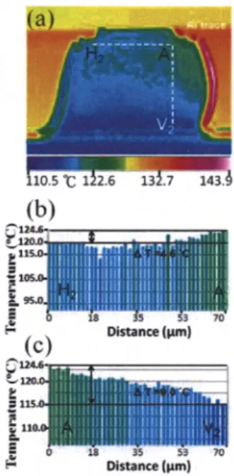
SnAg bump with a 5-Jlm Cu / 3-Jlm Ni UBM at 0.4 A . Fig. 1. IR images showing the temperature distribution and the temperature profiles along the dashed lines in the
SnAg bump with a 5-Jlm Cu / 3-Jlm Ni UBM at 0.2 A. As the applied current is increased, the hot spot became more pronounced. Figure 2(a) illustrates the thermographs when the bump was subjected to a 0.4 A current. A clear hot spot exists near the entrance of the current at the chip side. Figures 2(b) and 2(c) show the temperature
- -
-profiles along the dashed horizontal
AR
2and verticalAV
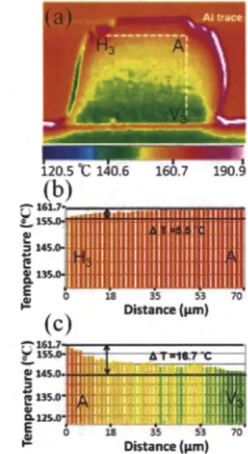
2 lines in Figure 2(a), respectively. The origin of Fig. 2(b) was set at point H2,whereas the origin of Fig. 2(c) was set at point A. The temperature difference increases to 4.6 °C and 9.0 °C along the horizontal and vertical line, respectively.When the stressing current is increased to 0.6 A, the hot spot became more significantly, as depicted in Figure 3(a). The horizontal temperature difference remains almost the same, whereas the vertical temperature difference continues to increase up to 16.7 °C, as illustrated in Figure 3(b) and 3{c). The origin of Fig. 3(b) was set at point H3,whereas the origin
of Fig. 3{c) was set at point A. A huge thermal gradient of 2392 °C/cm is developed across the solder bump. The thermal gradient is defined here as the temperature difference between the two ends of the dashed line divided by the length of the line, which was 70 Jlm for both the horizontal and vertical lines. The Joule heating effect also established a horizontal thermal gradient of 786°C/em.
5 3
Distance(1111\)
Hot spots start to emerge at a high density of approximately 3.5 x 10³A/cm2
. In this paper, we denote the existence of the hot spot when its temperature is 4.0 °C higher than the mean value in the solder bump, in which the mean temperature was obtained by averaging the values in a 50x50 Jlm2in the center of the bump. On the other hand, the hot-spot temperature was acquired by picking up the highest temperature in the region of interest. Figure lea) shows the temperature map distribution for the SnAg3.5 bump with a 5-Jlm Cu/3-5-Jlm Ni UBM during current stressing by 0.2 A. The temperature scale bar was shown in the x direction at the bottom of the figure. The current entered the solder bump through the Al trace on the chip end and it left the bump through the Cu line on the right-hand side of the substrate. The position of the Al trace was labeled in Fig. lea). The temperatures on the right and left edges of the bump may not be accurate since the image was taken at a prolonged exposure time of l5s and the sample may vibrate during the time span. The mean temperature in the bump was only 101.0 °C, which means that the average Joule heating was only 1.0 °C. However, there exist a hot spot in the solder bump. Figures l(b) and l(c) show the temperature profiles along the dashed
- -
-horizontal
ARt
and verticalAVt
lines in Figure 1(a), respectively. The origin of Fig. l(b) was set at point HI, whereas the origin of Fig. l(c) was set at point A. The horizontal line is located in the solder right below the NhS14 layer.Itshows that there is almost no temperature difference along the horizontal line, although there were small temperature fluctuations along the line. Since the temperature measurement by IR microscopy is very sensitive to surface roughness, the fluctuations may be due to surface roughness. However, there is about 3.8 °C difference in temperature along the vertical line. The hot-spot temperature was 105.6°C, which is located near the current entrance in the chip side into the bump. In this paper, this hot spot denote this location as hot-spot A. It - '--J'P Ii
I I 1'1: I: II I II I :III I:I I~ I III I I " II 14 II I II! j I: II II I 1III I III 18 35 53 10 Distance blln) 282Conclusions
In summary, two distinguished hot spots were observed in the bump when the applied current density is higher than 3.5x 10³ A/cm2 for the solder joints used in this study. Two
significant hot spots have been found: one at the region with peak current density, and the other one at the bump edge under the current-feeding metallization on the chip side. It is surprising that the latter has an even higher temperature than the former.
Acknowledgments
Place acknowledgments here, if needed. References
1. K. N. Tu, "Recent advances on electromigration in very-large-seale-integration of interconnects," J. Appl. Phys., Vol. 94, (2003), pp. 5451-5473.
2. International Technology Roadmap for Semiconductors, Semiconductor Industry Association, San Jose, CA (2003) 3. C. Y. Liu, Chih Chen, C.N. Liao, and K. N. Tu,
"Microstructure-electromigration correlation in a thin stripe of eutectic SnPb solder stressed between eu electrodes," Appl. Phys.Lett., Vol. 75, (1999), pp. 58-60. 4. Everett C.C. Yeh, W.1.Choi, and K. N. Tu,
"Electrochromic semiconductor nanocrystal films," Appl.
Phys.Lett., Vol. 80, (2002), pp. 4-6.
(b) Horizontal and vertical thermal gradients as a function of applied current with a 5-J.!m Cu / 3-J.!m NiUBM.
It is interesting that as the applied current increases, the vertical thermal gradient increases faster than that of the horizontal thermal gradient, as depicted in Figure 4(b). It appears that the horizontal thermal gradient did not increase much after 0.3 A. This may be attributed to the fact that the lateral heat conduction is better than that of the vertical direction, since Si has good heat dissipation ability.
Furthermore, it is surprising that another region with a lower local current density but possessed a temperature higher than the hot-spot value described above. The region is located in the right-hand side of the hot-spot and close to the underfill, as marked by one of the white squares in Figure 1(a). This region is denoted as hot-spot B in this paper. The three-dimensional electrical simulation in Figure 6 shows that the local current density is 2.17 x 10⁴ A/cm2, which is slightly lower than the value 2.46x 10⁴A/cm2in the region with peak current density. However, the average temperature there was as high as 167.8 °C, which is slightly higher than that at the hot spot with the maximum current density. The origin of this second hot spot may be attributed to two reasons: This region locates close to the Al trace, which serves as the major heating source in the joints. Secondly, it is adjacent to the underfill, which has much higher temperature than the solder bump, since the heat dissipation ability is the worst among the materials in the joints. The average temperature for the underfill close to the Al trace was as high as 179.2 °C. Hence, the solder adjacent to the underfill may possess a higher temperature, although it has lower local Joule heating.
70 190.9 :. 160.7 18 35 53 Distance (fun) l'fT'rl~T'11 I I'll I II IIII . 111111111111iI'll ','I: IIi1'1 111111111111111111" 11111 i IlllII111111'1111,1111111 ; I'llillllllllllllllllllll'! , 1,IIIIIIIIIIIIIIIII:llllIlltl 120.5
t:
140.6(b)
~16L71:.1
~14Se
&1 E ~(c)
c
i
w. .,:,~;':
•.~.
l!135.0 ,"r '0 ; & .~,1j:.::, '
E ",+,~~'
.-.. .: ••• QJ 0 18 3S 53 70 ... Distance(pm)Fig.3 IR images showing the temperature distribution and the temperature profiles along the dashed lines in the
SnAg bump with a 5-J.!m Cu / 3-J.!m Ni UBM at 0.6 A. Figure 4(a) shows the plot of average and hot-spot temperatures as a function of applied current densities/current with 5-J.!m Cu/3-J.!m Ni UBM. The applied current ranges from 0.1 to 0.6 A. With a higher current over 0.6 A, the solder bump may melt. The curve shows a parabolic behavior, which follows Joule heating relationship:
P= [2R=j2pv (2)
Where P is the heating power, [is the applied current, R is the resistance of the stressing circuit,j is the local current density, p is the resistivity, and v is the volume. In addition, the temperature difference between the average and hot-spot values becomes higher at a higher stressing current, which may be attributed to serious local Joule heating at the hot-spot.
AIPIM--(-"
11 .
;UIII'O' • .,0' ""...,0... 1...'0-tJx1O'"
e.-.t
OIl,..
wa,.a,... c.-..{Mpt
I..U lUI IU6 1M 1.51 I .•
_~ ...,... f) (b
1- ·-'.-...
0,· ~MII .I:J
l
·
~: -'~'
·
-i
I ~.• .' ~.
"""---~~--... 2."'0'~,olu •••)..~,.,0-
u.,rt C&wfWItD....,
CAIe-a.
Fig. 4. (a) Temperature increases in the hot-spot region and in the bump as a function of applied current with a 5-J.!m Cu / 3-J.!m Ni UBM.
5. T. L. Shao, Y. H. Chen, S. H. Chiu and Chih Chen, "Electromigration failure mechanisms for SnAg3.5 solder bumps onTi/Cr-Cu/CuandNi(P)/Aumetallization pads,"J.
Appl. Phys., Vol. 96, (2004), pp. 4518-4524
6. W.1. Choi, E. C. C. Yeh, and K. N. Tu, "Mean-time-to-failure study of flip chip solder joints on Cu/Ni(V)1Al thin-film under-bump-metallization,"J. Appl. Phys. Vol. 94, (2003), pp. 5665-5671.
7. Hua Ye, Cemal Basaran, and Douglas Hopkins, "Thermomigration in Pb-Sn solder joints under joule heating during electric current stressing," Appl. phys. Lett. Vol. 82, (2003), pp.l 045-1 047.
8. S. H. Chiu, T. L. Shao, and Chih Chen, "Infrared microscopy of hot spots induced by Joule heating in flip-chip SnAg solder joints under accelerated
electromigration," Appl. Phys. Lett., Vol. 88, (2006), pp. 022110-1-022110-3.
9. S. W. Liang, Y. W. Chang, and Chih Chen, "Effect of AI-trace dimension on Joule heating and current crowding in flip-chip solder joints under accelerated
electromigration, " Appl. Phys. Lett., Vol. 88, (2006), pp. 172108-1-172108-3.
10. H.Y. Hsiao and Chih Chen, "Thermomigration in flip-chip SnPb solder joints under alternating current stressing," Appl. Phys. Lett., Vol. 90, (2007), pp. 152105-1-152105-3.
11. Y-S Lai, K.M. Chen, C.L. Kao, C.W. Lee, Y.T. Chiu, "Electromigration ofSn-37Pb and Sn-3Ag-1.5Cu/Sn-3Ag-Q.5Cu composite flip-chip solder bumps with TilNi(V)/Cu under bump metallurgy," Microelectronics Reliability, Vol. 47, (2007), pp. 1273-1279.
12. J.R. Black, IEEE Trans. Electron Devices ED-16, 338 (1969).