Microstructural investigation of oxidized Ni/Au ohmic contact to p-type GaN
Li-Chien Chen, Fu-Rong Chen, Ji-Jung Kai, Li Chang, Jin-Kuo Ho, Charng-Shyang Jong, Chien C. Chiu, Chao-Nien Huang, Chin-Yuen Chen, and Kwang-Kuo Shih
Citation: Journal of Applied Physics 86, 3826 (1999); doi: 10.1063/1.371294
View online: http://dx.doi.org/10.1063/1.371294
View Table of Contents: http://scitation.aip.org/content/aip/journal/jap/86/7?ver=pdfcov Published by the AIP Publishing
Articles you may be interested in
Correlation between microstructure and temperature dependent electrical behavior of annealed Ti/Al/Ni/Au Ohmic contacts to AlGaN/GaN heterostructures
Appl. Phys. Lett. 103, 201604 (2013); 10.1063/1.4828839
Chemical, electrical, and structural properties of Ni/Au contacts on chemical vapor cleaned p-type GaN J. Appl. Phys. 91, 9151 (2002); 10.1063/1.1471578
Investigation of oxidation mechanism for ohmic formation in Ni/Au contacts to p-type GaN layers Appl. Phys. Lett. 79, 3815 (2001); 10.1063/1.1425065
Correlation of contact resistance with microstructure for Au/Ni/Al/Ti/AlGaN/GaN ohmic contacts using transmission electron microscopy
J. Appl. Phys. 89, 3143 (2001); 10.1063/1.1347003 Oxidized Ni/Pt and Ni/Au ohmic contacts to p-type GaN Appl. Phys. Lett. 76, 3703 (2000); 10.1063/1.126755
Jin-Kuo Ho, Charng-Shyang Jong, Chien C. Chiu, Chao-Nien Huang, Chin-Yuen Chen, and Kwang-Kuo Shih
Opto-Electronics and Systems Laboratories, Industrial Technology Research Institute, Chutung, Hsinchu, Taiwan 310, Republic of China
共Received 11 January 1999; accepted for publication 25 June 1999兲
The microstructure of oxidized Ni/Au films on p-GaN was examined to elucidate the formation of a low resistance ohmic contact to p-GaN with a field-emission gun transmission electron microscope in conjunction with composition analyses. The p-GaN/Ni/Au samples were heat treated at 500 °C in air mainly composed of a mixture of crystalline NiO, Au, and amorphous Ni–Ga–O phases. Small voids adjacent to the p-GaN film were also observed. The as-deposited Au film converted into discontinuous islands containing small amounts of Ni that connect with p-GaN. NiO formed a continuous film at the surface that covers the Au islands and the amorphous Ni–Ga–O phases. Moreover, NiO partially contacts p-GaN as well as Au islands and the amorphous Ni–Ga– O phase. The orientation relationship of the crystalline NiO, Au-rich islands, and p-GaN film was identified as NiO(111)//Au(111¯ )//GaN(0002) and NiO关11¯0兴//Au关11¯0兴//GaN关112¯0兴. The results suggested that Ni atoms diffuse through the Au layer onto the surface and react with oxygen to form NiO, whereas Au atoms diffuse towards the inside to form a Au–Ni alloy. The microstructural examination indicated that the crystalline NiO and/or the amorphous Ni–Ga–O phases may significantly affect the low resistance ohmic contact to p-GaN. © 1999 American
Institute of Physics.关S0021-8979共99兲05219-6兴
I. INTRODUCTION
The gallium nitride based semiconductor is one of the most promising materials for optoelectronic applications such as light emitting diodes共LEDs兲 and laser diodes 共LDs兲 in the blue and ultraviolet ranges. The recent development of high quality GaN crystalline film has resulted in rapid progress in the development of high brightness blue LEDs1 and continuous wave LDs at room temperature.2 However, such optoelectronic devices need low resistance ohmic con-tacts to both n- and p-type GaN to enhance their perfor-mance. Several approaches for constructing low resistance ohmic contacts to n-type GaN have been studied.3–8 The most widely used ohmic contacts to n-type GaN are based on an Al/Ti bilayer.3–6Related investigations proposed the for-mation of reaction phases such as Al–Ti intermetallics,3,4 TiN,4,5and AlN 共Refs. 5 and 6兲 to induce low specific con-tact resistance ranging between 10⫺6 and 10⫺7⍀ cm2. In contrast to the great amount of attention paid to n-type GaN contact, low resistance ohmic contact to p-type GaN has meet with less success. Specific contact resistance to p-GaN was restricted to 10⫺2– 10⫺3⍀ cm2. Such a high value is insufficient for high performance device applications. The
major restrictions in achieving low resistance ohmic contacts to p-type GaN is that the carrier concentration of p-GaN cannot be increased to a degenerated level, and a practical metal with a high work function is not available. The carrier concentration of p-GaN prepared by epitaxial growth is gen-erally limited to about 1018cm⫺3.9,10 Other methods, e.g., diffusion11,12and ion implantion,13–16 were also applied to increase the carrier concentration. However, no significant improvement has been achieved. Thus, metallic materials with a high work function are expected to alleviate the resis-tance. Multilayer metallic films with a high work function, such as Ni/Au,17–21Pt/Au,22 and Pt/Ni/Au,23are extensively used as contacts to p-type GaN.
Recently Ho et al.21successfully developed a contact to
p-type GaN with a specific contact resistance lower than 1 ⫻10⫺4⍀ cm2 using an oxidizing Ni 共10 nm兲/Au 共5 nm兲 metallization scheme.21 This value is approximately one to two orders of magnitude lower than any contact resistance previously reported. They attributed the low resistance ohmic contact to the formation of NiO. These excellent elec-trical properties promoted this detailed investigation of the microstructure of as-deposited and oxidized Ni/Au films on
p-GaN to analyze the phase evolution of alloys that correlate
with low contact resistance to p-type GaN. Furthermore, the
a兲Electronic mail: [email protected]
3826
0021-8979/99/86(7)/3826/7/$15.00 © 1999 American Institute of Physics
reaction mechanism and diffusion behavior are also dis-cussed in this study.
II. EXPERIMENT
Sapphire/undoped GaN共2 m兲/Mg-doped GaN 共2 m兲 samples were prepared by metalorganic chemical vapor deposition 共MOCVD兲. Trimethylgallium and ammonia were used as the sources of Ga and N, respectively. The sapphire substrates were cleaned with organic solvents before they were loaded into the MOCVD system. A low temperature GaN nucleation layer was initially grown on the sapphire substrates, and 2 m undoped GaN and 2 m Mg-doped GaN were subsequently grown at about 1000 °C. Heat treat-ment of the GaN samples in N2atmosphere at suitable tem-perature was used to activate the Mg atoms to the p-type dopant. The results of Hall measurement showed that the hole concentration of p-GaN was 2⫻1017cm⫺3. Prior to metal deposition, the samples were etched with HCI:H2O
⫽1:1 for 1 min to remove native oxide, and then 10 nm Ni
and 5 nm Au were deposited on the p-type GaN as metal contacts by electron beam evaporation under a base pressure that was lower than 3⫻10⫺6Torr. We then oxidized the as-deposited Ni/Au sample at 500 °C in air for 10 min to induce interdiffusion of the bi layer metals共Ni and Au兲 and reaction with oxygen. Thus a low resistance ohmic contact to
p-GaN was obtained.
Microstructural and compositional analyses were per-formed using a JEOL 2010F field emission gun transmission electron microscope共FE-TEM兲 equipped with an Oxford en-ergy dispersive x-ray spectrometer共EDS兲 and a Gatan image filter 共GIF兲. Elemental mappings and high-resolution elec-tron energy loss spectroscopy共EELS兲 spectra were both ob-tained by the GIF system. Crystal structure identification, EDS, and EELS were carried out using a 0.5 nm nanobeam probe. Cross-sectional TEM samples were prepared by the tripod polishing method. Then the TEM samples were mounted on Cu grids and ion milling followed.
III. RESULTS AND DISCUSSION
The as-deposited Ni and Au films were polycrystalline with a small grain size of few nanometers, as depicted in Fig. 1. The Ni layer was grown in a column-like structure on
p-GaN with the preferred orientation, Ni共002兲//GaN共0002兲.
The subsequently deposited Au layer was built epitaxially on the Ni layer, and had an ambiguous interface. No interlayer between Ni and p-GaN was observed. This finding indicates that the sample precleaning and subsequent deposition caused no contamination or reaction between the interface of Ni and p-GaN; this is different from the results reported by Bermudez et al.,24 who observed reaction even near room temperature. However, in current–voltage measurement, the as-deposited sample showed a rectifying characterisic.21 Heat treatment of the as-deposited samples in N2or in form-ing gas did not change the rectifyform-ing characteristic.
After an oxidizing treatment at 500 °C in air, the bilayer metals reacted with oxygen and were transformed into a new microstructure that makes the contact ohmic with low inter-face resistance.21 Figure 2共a兲 displays a typical microstruc-ture of the oxidized sample in cross-sectional view. Discrete crystalline islands with darker contrast were observed; the amorphous phase and voids existed among the crystalline grains. A nonuniform crystalline thin film with an uneven surface covered these features. High-resolution TEM and EDS analyses were performed to examine in detail the com-position and microstructure of these phases. These results are shown in Figs. 2共b兲, 3, and 4. Figure 2共b兲 is a magnified micrograph of the typical oxidized sample. The EDS spectra and the diffraction patterns, depicted in Figs. 3 and 4, respec-tively, correspond to the points marked ‘‘a,’’ ‘‘b,’’ and ‘‘c’’ in Fig. 2共b兲. Both the EDS spectra and the diffraction pat-terns were obtained using a 0.5 nm electron probe. Figure 3共a兲 presents the EDS spectrum from point ‘‘a’’ of the dis-continuous island of Fig. 2共b兲; this spectrum indicates that the island primarily consists of Au, with a small amount of
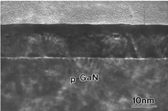
FIG. 1. Typical cross-sectional TEM image of the as-deposited
p-GaN/Ni/Au sample.
FIG. 2. TEM micographs of p-GaN/Ni/Au samples after an oxidizing treat-ment at 500 °C for 10 min in air. 共a兲 Low magnification image and 共b兲 high-resolution image.
3827
J. Appl. Phys., Vol. 86, No. 7, 1 October 1999 Chenet al.
Ni. Figure 4共a兲 shows the diffraction pattern from the same point that is consistent with the Au structure. The results identify the discrete islands as Au-rich grains. Conversely, the crystalline film above the Au islands was mainly com-posed of Ni and O, as illustrated by the EDS spectrum in Fig. 3共b兲, which was obtained from point ‘‘b’’ in Fig. 2共b兲. This film was further confirmed as being a face-centered-cubic NiO phase by a nanobeam diffraction pattern depicted in Fig. 4共b兲. Some inclined twins were observed in the crystalline NiO film, as indicated by an arrow in Fig. 2共b兲. These
de-fects are commonly seen in the face-centered-cubic structure. The EDS analysis, illustrated in Fig. 3共c兲 from point ‘‘c’’ of Fig. 2共b兲, displays the amorphous regions consisting of a relatively larger amount of Ga as well as Ni and O. The EDS semiquantification analysis indicated that the Ga:Ni atomic ratio is about 2:1. The orientation relationships among
FIG. 3. EDS spectra obtained from points共a兲 ‘‘a,’’ 共b兲 ‘‘b,’’ and 共c兲 ‘‘c’’ of Fig. 2共b兲, respectively.
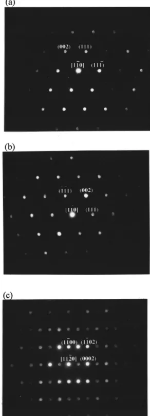
FIG. 4. Nanobeam diffraction patterns obtained from points共a兲 ‘‘a’’ and 共b兲 ‘‘b’’ of Fig. 2共b兲, and from 共c兲 the p-GaN film, respectively. The diffraction patterns identify the phases as共a兲 Au, 共b兲 NiO with a face-centered-cubic structure in the关110兴 zone axis, and 共c兲 GaN with a close-packed-hexagonal structure in the关1120兴 zone axis.
the NiO film, the Au islands, and the p-GaN are deter-mined from the nanobeam diffraction patterns illustrated in Fig. 4. These orientation relationships are given as NiO(111)储Au(111¯ )储GaN储(0002) and NiO关11¯0兴储
Au关11¯0兴储GaN关112¯0兴.
The preceding results give the following implications. During annealing at 500 °C in air, interdiffusion of Ni and Au atoms occurred. It is conceivable that grain boundaries25 of the as-deposited Au film may serve as quick diffusion channels for outdiffusion of Ni atoms to the surface at this temperature. The driving force for the Ni atoms diffusing out through the Au layer results from the stronger affinity of Ni to O than that of Au to O. During the outdiffusion of Ni atoms to the surface, interdiffusion between Ni and Au at-oms at the interface also occurred, and this could lead to the formation of the Ni–Au alloy. According to the Ni–Au phase diagram,26the equilibrium concentration of the Au–Ni alloy at 500 °C is 5% Ni–Au or 93% Ni–Au as a result of the miscibility gap. The EDS quantification indicates that the concentration of Ni in Au-rich islands is much less than 5% or even that there was no Ni detected in the Au islands. This suggests that the Ni in the Ni–Au alloy is steadily consumed as a consequence of the oxidation of Ni at the surface. Thereby, little Ni is left in the Au-rich islands and the NiO film is constructed on the top of the Au-rich islands.
After oxidation, the Au-rich islands were sandwiched by the NiO and GaN, which results in forming two new inter-faces of Au/NiO and GaN/Au. The equilibrium contact angle between the Au islands with GaN was about 120°–140° due to the balance of surface energy among the GaN, and NiO or the amorphous Ni–Ga–O phase. The average thickness of Au-rich islands also changed to approximately 10 nm, that is, to double the as-deposited thickness. Thereby, the small
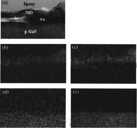
FIG. 5. Electron energy filtering mapping of the oxi-dized Ni/Au film.共a兲 Zero loss image with a 50 eV slit width,共b兲 Ni mapping, 共c兲 O mapping, 共d兲 Ga mapping, and共e兲 N mapping.
FIG. 6. Electron energy loss spectra of crystalline NiO and the amorphous Ni–Ga–O phase.共a兲 Oxygen K edge and 共b兲 Ni L edge.
3829
J. Appl. Phys., Vol. 86, No. 7, 1 October 1999 Chenet al.
voids observed in Fig. 2共b兲 may have appeared as a conse-quence of conserving the constant volume of Au. The forma-tion of voids reduced the contact area to p-GaN after oxida-tion, which could degrade the contact performance.
The energy filtering mapping images, depicted in Fig. 5, provided an overall picture of the compositional distribution of the oxidation process. Figures 5共a兲–5共e兲 display the zero loss image, and the Ni, O, Ga, and N elemental mappings, respectively. The width of the selected energy window ranged from 30 to 50 eV according to the energy loss. The energy window was centered on the energy loss levels of 855, 532, 1115, and 400 eV for Ni, O, Ga, and N mappings, respectively. The bright contrast in the Ni and O mappings was consistent with the EDS analysis 共Fig. 3兲; this bright contrast was identified as the crystalline NiO and amorphous regions. On the other hand, Au islands showed darker con-trast in these two mappings. Furthermore, the Ga mapping displayed a diffusive Ga interface, in contrast to a sharper interface from N mapping. This suggests that GaN dissoci-ated into Ga and N after the heat treatment. The Ga atoms are distributed near the interface, but the N atoms might
diffuse out or join the voids. Because the intensity of the Ga signal in the amorphous region of the Ga mapping is com-parable to the noise, no useful information could be ex-tracted.
More atomic information of crystalline NiO and the amorphous Ni–Ga–O phase was obtained from EELS, as depicted in Fig. 6. The electron core energy loss of the oxy-gen K edge is near 532 eV, and that from the Ni L edge is about 855 eV. Figures 6共a兲 and 6共b兲 present the oxygen
K-edge electron energy loss near edge structures 共ELNES兲
following background subtraction and the Ni L-edge ELNES, respectively. The oxygen K-edge ELNES of crys-talline NiO is obviously different from that of the amorphous Ni–Ga–O phase. The initial 5–10 eV from the threshold of the oxygen spectra contains information on the O 2 p orbital hybridizing with the Ni 3d levels.27,28The first edge of oxy-gen ELNES of the crystalline NiO, indicated by an arrow in Fig. 6共a兲, disappears in the amorphous Ni–Ga–O phase. This kind of edge is associated with the existence of unoccupied states of mixed O 2 p with Ni 3d orbitals. Correspondingly, oscillations of 5 or 10 to about 30 eV from the threshold of
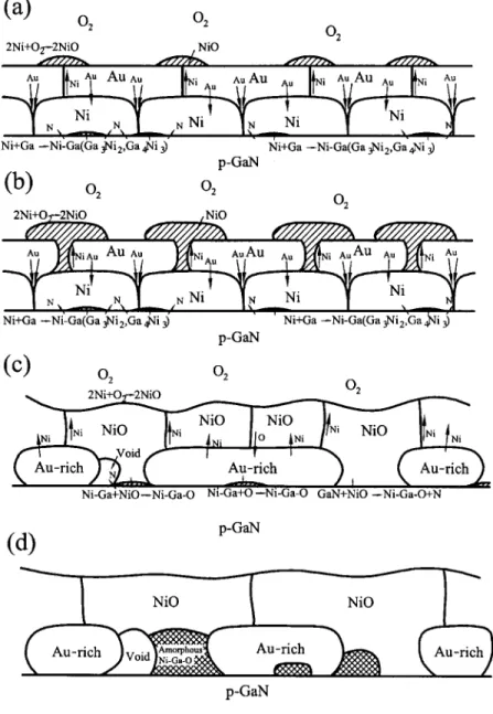
FIG. 7. Schematic illustration of the reaction mecha-nism and diffusion behavior during the oxidation of
p-GaN/Ni/Au.共a兲 Early stage of oxidation reaction, 共b兲
pronounced interdiffusion and crystalline NiO grow up to separate the Au–Ni alloy into discrete islands,共c兲 Au-rich islands building epitaxially on p-GaN and three possible reactions producing Ni–Ga–O phases, and共d兲 oxidized contact scheme with optimum phase distribution.
the ELNES reflect the local atomic environment. The differ-ence in ELNES between the crystalline NiO film and the amorphous Ni–Ga–O phase indicates the change in atomic bonding and valence state. EELS quantification analysis also shows that the Ni:O ratio of amorphous Ni–Ga–O regions is 10% lower than that of the crystalline NiO area. The com-positional distribution might also significantly influence the electric properties.
Consequently, we believe that, during oxidation, some Ni atoms initially diffuse into the Au layer, enriching at the grain boundaries and, then, propagate to the surface to react with oxygen to form NiO. At the same time, the Ni left behind reacts with GaN to form the Ni–Ga alloy, Ga4Ni3, and Ga3Ni2.20,24When the NiO grows down to contact the Ni/GaN reaction products, such as the Ni–Ga alloy, Ga4Ni3, and Ga3Ni2,20,24a new oxidation reaction again takes place and an amorphous Ni–Ga–O phase forms with the liberation of N2 to air or to the voids. According to the preceding results, a reaction mechanism is proposed to interpret the oxidation behavior of the Ni/Au contact to p-GaN; it is il-lustrated in Fig. 7. In the preliminary stage of oxidation, depicted in Fig. 7共a兲, Ni atoms start to diffuse out through the Au layer, primarily through grain boundaries, to react with oxygen and Au atoms that diffuse into the Ni layer to form the Au–Ni alloy. At the same time, the interfacial re-action between GaN and Ni may result in the formation of the Ga–Ni alloy and/or intermetallic compounds such as Ga4Ni3 and Ga3Ni2.20,24 The progression of the diffusion, depicted in Fig. 7共b兲, further promotes the oxidation of Ni. The crystalline NiO grows up to separate the Au–Ni alloy into discrete islands. In the next stage, as illustrated in Fig. 7共c兲, the Au-rich islands migrate inside and epitaxially build on p-GaN while the NiO also grows down to contact the GaN or Ni–Ga products. Three possible reactions are attrib-uted to the production of the amorphous Ni–Ga–O phase. First, the oxidation of GaN may occur when the NiO grows down to the interface. Second, the NiO may also react with the Ga–Ni alloy or with intermetallic compounds. Moreover, the oxygen atoms can diffuse through the boundaries be-tween the Au-rich island and NiO or the amorphous Ni– Ga–O phase and react with the Ni–Ga product when the Ni–Ga product is under the Au-rich island. The nitrogen released from the reaction may diffuse out or join the voids and probably results in the loose structure of the amorphous phases. Ultimately, as demonstrated in Fig. 7共d兲, the discon-tinuous Au-rich islands, amorphous Ni–Ga–O phase, and some voids are sandwiched between crystalline NiO and the
p-GaN film.
Although the stoichiometric crystalline NiO is an insu-lator, the NiO is found to be a p-type semiconductor while increasing Ni3⫹ ions by introducing Ni2⫹ vacancies and/or interstitial oxygen.29 The low specific contact resistance of the oxidized Ni/Au metallization scheme was attributed to the high conductivity of Au islands and the low contact bar-rier of p-NiO to p-GaN.21 However, this investigation dis-covered two products, the amorphous Ni–Ga–O phase and crystalline NiO contacting p-GaN. Whether one, or both, of these products is responsible for reducing the interface im-pedance still remains unclear at this time. Further studies
will continue to elucidate this formation of low resistance ohmic contact to p-GaN.
IV. CONCLUSIONS
Very low specific contact resistance to p-type GaN, lower than 1⫻10⫺4⍀ cm2, was attained by oxidizing Ni/Au bilayer metallization. The microstructural evolution of oxidized Ni 共10 nm兲/Au 共5 nm兲 ohmic contact to p-type GaN was investigated. During oxidation, Ni diffused out through the Au layer to react with oxygen and thus form crystalline NiO. Ni was steadily consumed in the oxi-dizing reaction. The epitaxial orientation relationship of crystalline NiO, the Au-rich island, and p-type GaN were determined to be NiO(111)储Au(111¯ )储GaN储(0002) and NiO关11¯0兴储Au关11¯0兴储GaN关112¯0兴. Crystalline NiO and the amorphous Ni–Ga–O phase were also found. EELS analysis demonstrated the different atomic bonding and valence states between crystalline NiO and the amorphous Ni–Ga–O phase. The results suggest that crystalline NiO and/or the amorphous Ni–Ga–O phase may play a significant role in lowering ohmic contact resistance to p-type GaN.
ACKNOWLEDGMENTS
Partial support of this work by the Ministry of Economic Affairs of Republic of China under Contract No. 88-EC-2-A-17-0164 is gratefully acknowledged.
1S. Nakamura, T. Mukai, and M. Senoh, Appl. Phys. Lett. 64, 1687共1994兲. 2S. Nakamura, M. Senoh, S. Nagahama, N. Iwasa, T. Yamada, T.
Mat-sushita, Y. Sugimoto, and H. Kiyoku, Jpn. J. Appl. Phys., Part 2 36, L1130共1997兲.
3M. E. Lin, Z. Ma, F. Y. Huang, Z. F. Fan, L. H. Allen, and H. Morkoc¸,
Appl. Phys. Lett. 64, 1003共1994兲.
4S. Ruvimov et al., Appl. Phys. Lett. 69, 1556共1996兲. 5
B. P. Luther, S. E. Mohney, T. N. Jackson, M. A. Khan, Q. Chen, and J. W. Yang, Appl. Phys. Lett. 70, 57共1997兲.
6B. P. Luther, S. E. Mohney, J. M. Delucca, and R. F. Karlicek, Jr., J.
Electron. Mater. 27, 196共1998兲.
7Z. Fan, S. N. Mohammad, W. Kim, O¨ . Aktas, A. E. Botchkarev, and H.
Mokoc¸, Appl. Phys. Lett. 68, 1672共1996兲.
8J. Burn, K. Chu, W. A. Davis, W. J. Schaff, L. F. Eastman, and T. J.
Eustis, Appl. Phys. Lett. 70, 464共1997兲.
9H. M. Ng, D. Doppalapudi, D. Korakakis, R. Singh, and T. D. Moustakas,
J. Cryst. Growth 349, 189共1998兲.
10
S. Nakamura and G. Fasol, The Blue Laser Diode共Springer, New York, 1997兲.
11T. Kim, M. C. Yoo, and T. Kim, Mater. Res. Soc. Symp. Proc. 449, 1061
共1997兲.
12
L. L. Smith, M. D. Bremser, E. P. Carlson, T. W. Weeks, Jr., Y. Huang, M. J. Kim, R. W. Carpenter, and R. F. Davis, Mater. Res. Soc. Symp. Proc. 395, 861共1996兲.
13B. Menschubg, C. Liu, B. Rauschenbach, K. Kornitzer, and W. Ritter,
Mater. Sci. Eng., B 50, 105共1997兲.
14
R. G. Wilson, C. B. Vartuli, C. R. Abernathy, S. J. Pearton, and J. M. Zavada, Solid-State Electron. 38, 1329共1995兲.
15J. C. Zolper, R. G. Wilson, S. J. Pearton, and R. A. Stall, Appl. Phys. Lett. 68, 1945共1996兲.
16
M. Rubin, N. Newman, J. S. Chan, T. C. Fu, and J. T. Ross, Appl. Phys. Lett. 64, 64共1994兲.
17G. Mohs, B. Fluegel, H. Giessen, H. Tajalli, and N. Peyghambarian, Appl.
Phys. Lett. 67, 1515共1995兲.
18S. Nakamura, M. Senoh, S. Nagaham, N. Iwasa, T. Matsushuta, H.
Kiy-iku, and Y. Sugimoto, Appl. Phys. Lett. 68, 3269共1996兲.
19H. Ishikawa, S. Kobayashi, Y. Koide, S. Yamasaki, S. Nagai, J. Umezaki,
M. Koike, and M. Murakami, J. Appl. Phys. 81, 1315共1997兲.
3831
J. Appl. Phys., Vol. 86, No. 7, 1 October 1999 Chenet al.