Low-Cost LED Driver
Chun-Yu Hsieh and Ke-Horng Chen, Senior Member, IEEE
Abstract—An RGB LED driver with the fast reference tracking
(FRT) and charge-recycling (CR) techniques is proposed to imple-ment a high-efficiency and low-cost RGB backlight module in color sequential notebook computers’ display. The proposed LED driver composed of an asynchronous 1.5 MHz DC/DC boost converter with the FRT and CR techniques was fabricated in TSMC 0.25 m BCD 40 V technology to generate 16 V for 6-series red (R) LEDs or 21 V for 6-series green (G), or blue (B) LEDs. The FRT technique can speed up the reference tracking performance and effectively improve the up-tracking performance. However, the down-refer-ence tracking depends on the load current and output capacitor. It is difficult to enhance the transient response without reducing the efficiency. Therefore, the CR technique is proposed to store extra energy on the recycling capacitor when the output voltage is switched from high- to low-supplying voltage level and releases the reserved energy back to the output node at next period. Fur-thermore, the output voltage can be rapidly switched between two different voltage levels by FRT technique without consuming much power owing to the restored energy by the CR technique. Exper-imental results show that the total power consumption of a note-book computer’s 15.4’ LCD panel can be reduced from 5 W in cold-cathode fluorescent lamp (CCFL) backlight module to about 2-3 W in RGB LED backlight module with the field color sequen-tial (FCS) algorithm. Furthermore, after the implementation of the LED driver with the FRT and CR techniques, the power loss can be reduced to about 24% of that without the FRT and CR techniques.
Index Terms—Charge recycling, feedforward technique, field
color sequential, LCD, LED backlight, reference tracking.
I. INTRODUCTION
F
OR high-quality display in LCD panels, the selection of the backlight module becomes more and more important. The selection of backlight system not only affects the power consumption but also determines display quality. Today’s most popular and power-efficiency backlight module is the white-LED backlight in LCD panels since the power dissipation can be reduced about 40% compared to conventional CCFL backlight module. Moreover, since the backlight module willManuscript received October 22, 2008; revised March 05, 2009. Current ver-sion published August 26, 2009. This work was supported by the National Sci-ence Council of Taiwan under Grant NSC 97-2221-E-009-172, and also by RichTek Technology Corporation and Chunghwa Picture Tubes, Ltd.
The authors are with the Department of Electrical Engineering, National Chiao Tung University, Hsinchu, Taiwan (e-mail: [email protected]).
Color versions of one or more of the figures in this paper are available online at http://ieeexplore.ieee.org.
Digital Object Identifier 10.1109/JSSC.2009.2024051
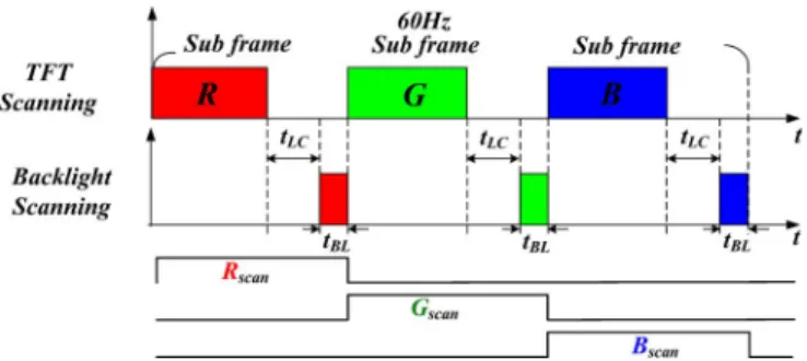
Fig. 1. The timing diagram of color sequential technique for the color filterless LCD panel.
affect the color gamut, it is popular to make the use of LED backlight in the LCD panels due to the higher color gamut. That is, the white-LED backlight has better color gamut than that of the cold-cathode fluorescent lamp (CCFL) backlight. The dis-advantage of the white-LED backlight is that it still needs the color filter to determine the color of the images since the opera-tion of liquid crystal only determines the gray level of the image. In addition, the white-LED backlight generates only 70%–80% National Television System Committee (NTSC) color gamut. In order to have better color gamut, the technique that uses RGB LED backlight for improve the color gamut, which is about 110% NTSC, becomes a trend of today’s LCD display market [1], [2].
According to the display method of the LCD panel, the liquid crystal, which is functioned as a gate, is turned to the position determined by the content of the display data. Then, the light from backlight module only pass one of three color filters to de-termine the correct color by the operation of the liquid crystal according to the image data. Therefore, the power loss due to the color filter is relatively large and the power consumption of the backlight module is difficult to be decreased because a lot of light is blocked by the color filter. Certainly, the best method is to remove the usage of the color filter. Recently, the field color sequential (FCS) algorithm [3] that effectively reduced color breakup and motion blur effects can save much power consumption of the backlight module without the requirement of color filter. Conceptually shown in Fig. 1, the conventional color sequential algorithm effectively reduces power consump-tion without sacrificing the color gamut because the LEDs are not turned on simultaneously but sequentially. One frame data operated by the rate of 60 Hz is divided into three sub-frames, which are , , and . Thus, the rate of the three
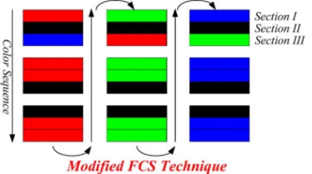
Fig. 2. The implementation of modified FCS algorithm for reducing the color breakup and improving the efficiency.
sub-frames is 180 Hz. For each sub-frame, the first step is the operation of thin film transistor (TFT) scanning for reading the image data. According to the image data, liquid crystal is turned to the correct position within time . This step occupies the most of sub-frame time. When liquid crystal is turned to the suitable position, the LED backlight module emits correct light through the LCD panel to display correct image color. The rest of time , which represents the lightening time for backlight module, can determine the value of brightness. However, the value of time is too small to provide the rated brightness since one frame is divided into three sub-frames. In order to ex-tend the lightening time of backlight module, there are many techniques proposed [2]–[5] in high-performance color sequen-tial display to achieve full color image. Furthermore, the modi-fied FCS algorithm inserts black data and disrupts the color se-quence to reduce the color breakup effect in the temporal and spatial domain. First, the implementation of modified FCS algo-rithm is to divide the LED panel to small divisions in the vertical directions to achieve a low-resolution LED panel for lighting the high-resolution LCD panel. In each division, the circulation is in the sequence of the color red, green, blue and black. Besides, the sequence order of each area is different. The modified FCS algorithm divides the full color picture into three divisions in spatial domain owing to the small-size panel of the notebooks and divides one frame into nine sub-frames in the temporal do-main as shown in Fig. 2. In addition, the purpose of the insertion of black data is to prevent the color data from being mixed by other colors. Therefore, FCS algorithm can effectively reduce power consumption of RGB LED backlight module compared to the white-LED backlight module with compatible brightness, thereby becoming the most power-efficiency technique in the design of backlight modules of the LCD panel.
The comparison of power consumption between a conven-tional TFT-LCD with a white-LED backlight module and a FCS TFT-LCD with an RGB LED backlight module is illustrated in Fig. 3. Interestingly, the FCS algorithm can save 40% power compared to the conventional LCD display because there is no color filter that may reduces the brightness in the front of the LCD panel. Hence, the power consumption of the backlight module can be drastically minimized. Furthermore, this nique can be extended to contain the blanking/dimming tech-nique according to the locally averaged image data. That is, a higher power saving result can be achieved and thus the power reduction can be more than 60%. Actually, the minimum power consumption of the LCD display can be reduced to 20% of the
Fig. 3. The power consumption with different display techniques.
conventional design when the backlight system is turned off. However, the image only contains gray levels at this moment. For portable devices like notebook computers, the largest power consumption comes from the backlight module. The power con-sumptions in the recently LCD panels are reduced to 5 W in white LED backlight and 3 W in color sequential RGB back-light system, respectively, compared to 6 W in CCFL backback-light. Therefore, it is important to decrease the power consumption in backlight module of the notebooks without sacrificing any image quality. However, the drawback of the FCS algorithm is the color breakup effect when the RGB LEDs emit light in se-quence. Furthermore, the RGB backlight module employs im-pulse-type display method instead of the hold-type display by CCFL backlight technique for eliminating the motion blur [1]. The disadvantages of the conventional FCS algorithm can be al-leviated by the implementation of the modified FCS algorithm. The light illumination of LED is related to the amount of driving current and the forward voltage [6], [7]. However, it is unreliable that the light illumination is controlled by utilizing the forward voltage when temperature and time is changed [8], [9]. That is, it is inappropriate to make use of forward voltage to control the brightness of LED for getting high-quality image of LCD panel. In order to get uniform and sufficient lumi-nance, the LCD backlight module requires many LEDs to be series-and parallel- connection. The series connection ensures the series LEDs have the same conduction current. The parallel connection needs a current balance (CB) circuit to maintain stable and uniform light illumination in every series connection as shown in Fig. 4. The DC-DC converter is used to offer a sufficient voltage to overcome all the forward voltage of series LEDs. Owing to the great variation of LED material, each of the series LEDs forward voltage is different. Hence, the current balance circuit is designed as the current of LED that is independent of the voltage , which is the voltage across the current balance circuit. In general, the LED module will minimize the voltage [8], [9] for reducing the power consumption because the power consumption is equal to the product of and . If the output voltage is larger than , the redundant voltage will be across the cur-rent balance circuit. Therefore, the power loss will be increased and the efficiency of the LED array, which depends on the ratio of the and the , will be decreased. In order
Fig. 4. Power consumption of the current balance circuit.
to improve the efficiency of LED backlight module, the value of the voltage must be minimized and the variation of the voltage will not affect the driving current .
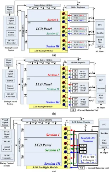
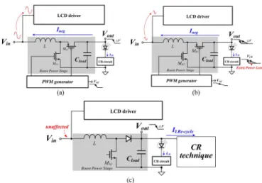
In general, the forward voltages of red, green, and blue LEDs are different to each other owing to the characteristic of material. That is, the forward voltage of a red LED is approximately 2.5 V and the forward voltage of a green/blue LED is about 3.5 V [10]. For a 6-series R-LED branch, a boost DC-DC converter is needed to step up the supply voltage to about 16 V. Similarly, two separate boost DC-DC converters are required to boost the supply voltage to about 21 V for two 6-series green-LED and blue-LED branches. Therefore, the LEDs with different colors require different supplying voltages [11]. That is, the imple-mentation of the LED driver of the modified FCS algorithm needs nine DC-DC converters for driving the notebook’s panel with the advantages of much power saving on the current bal-ance circuit. This expensive backlight module system is illus-trated in Fig. 5(a) [12]–[15]. This paper proposes a new imple-mentation of the RGB backlight module depicted in Fig. 5(b) for achieving low cost and high efficiency. It is obvious that only three DC-DC converters with current balance circuit are needed. The hardware cost and volume can be effectively re-duced. Since the bandwidth of the boost converter is limited to the low-pass filter which is composed of the inductor and capacitor, the fast switching output voltage between 16 V and 21 V is very difficult in the conventional DC-DC boost con-verters. In order to effectively reduce the chip cost and footprint area, the implementation of fast FRT and CR techniques is uti-lized. The FRT technique can make the LED driver drives more than 6-series R- and G-/B-LEDs by fast increasing or decreasing the output voltage to correct voltage level. Furthermore, the CR technique is presented to store the extra energy when the output voltage is decreased from high-supplying voltage level for 6-series G-/B-LEDs to low-supplying voltage level for 6-se-ries R-LEDs. Therefore, the CR technique can quickly decrease the output voltage and the stored energy can be sent back to the output node for rapidly increasing the voltage level back to the high-supplying voltage level. Therefore, the proposed LED driver with FRT and CR techniques achieve high-efficiency con-version and low-cost performance compared to the conventional design. Moreover, three DC-DC converters can be decreased to only one DC-DC converter at the sacrifice of power consump-tion. In Fig. 5(c), the CR mechanism is disabled and the output voltage is always stepped up to about 21 V for driving 6-series R, G, or B LEDs. Considering the case of the 6-series R-LEDs, if the output voltage is 21 V instead of 16 V, it will cause a large redundant voltage across the current balance circuit and
Fig. 5. (a) Conventional RGB LED backlight with nine DC-DC converters. (b) A high-efficiency RGB LED backlight with three DC-DC converters (c) A low-cost RGB LED backlight with only one DC-DC converter.
thus the efficiency is reduced. Therefore, the structure dissi-pated in Fig. 5(c) consumes more power than that in Fig. 5(b). Thus, a low-cost design methodology is presented for further re-ducing the external components and footprint area in RGB LED backlight module. Namely, the design methodology in Fig. 5(b) achieves a high-efficiency performance compared to Fig. 5(c). Nevertheless, the structure in Fig. 5(c) achieves low-cost imple-mentation compared to Fig. 5(b).
An integrated LED driver with FRT, CR techniques, and cur-rent balance circuit is presented in this paper. In the Section II, the analysis of the reference tracking procedure with FRT and CR technique is presented. The FRT technique is utilized for rapidly switching between two different output voltages and the CR technique is proposed for saving much power dissipation during the transition between two different output voltages. Fur-thermore, the stability and transient response of the LED driver with FRT technique is also discussed in this section. Section III describes the circuit implementation composed of the voltage control current source (VCCS) compensator, the PWM gener-ator, and the one-shot generator. Besides, the design of the cur-rent balance circuit is introduced to describe the power reduc-tion due to the implementareduc-tion of FRT and CR techniques. The
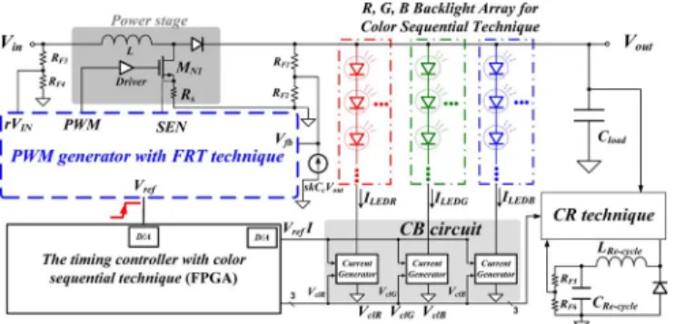
Fig. 6. The proposed LED driver contains the FRT, CR techniques, and the current balance (CB) circuit.
chip was fabricated in TSMC 0.25 m BCD 40 V technology and experimental results are discussed in Section IV. Finally, a conclusion is made in Section V.
II. THEANALYSIS OFFRT TECHNIQUE ANDCR TECHNIQUE
The LED driver for FCS algorithm needs two characteristics to meet the requirements of the LCD response time. One is the fast reference voltage tracking [16], [17] for rapidly switching output voltage to meet the requirement of three colors LEDs and the other one is the charge-recycling [18], [19] for reducing power consumption. The schematic of the proposed RGB driver is shown in Fig. 6. The main blocks contain the PWM gener-ator with FRT technique, the CR circuit, the CB circuit, and the timing controller implemented by FPGA.
A. The Operation Principle of the FRT Technique
The function blocks of PWM generator with FRT technique is shown in Fig. 7(a). The correction current generated by the amplifier represents the output voltage condition of the LED driver. Owing to the usage of the amplifier, the char-acteristic of high bandwidth can result in fast load/line transient response and reference tracking. However, the static error is worse since the characteristic of low gain of the amplifier. Therefore, the FRT technique utilizes the feedforward current to minimize the effect of for improving the static per-formance. Furthermore, the feedforward current standing for the input voltage information also can improve line transient performance. The output of the sawtooth generator is a saw-tooth waveform with a high threshold current defined as and a low threshold current defined as “0”. There-fore, the sawtooth signal with reference voltage information can rapidly determine the value of the duty cycle, thereby regulating the output voltage to quickly track the variations of the reference voltage .
The duty cycle of a voltage-mode LED driver operated in con-tinuous current mode (CCM) is defined as (1) and depicted in Fig. 7(b). At steady state, the correction current can be ne-glected because the feedforward current is used to mini-mize the value of correction current . The static performance
Fig. 7. (a) The PWM generator with FRT technique. (b) The determination of duty waveform in the PWM generator with FRT technique.
can be improved since the duty cycle of LED driver with FRT technique can be simplified as (2).
(1) (2) When the LED driver is well-designed, the feedback voltage is equal to the reference voltage as shown in (3). According to (2) and (3), the expression of the duty cycle is rewritten as (4). It is obvious that the transient response of line/load can effec-tively improved due to the appearance of the input and output information in (4). Therefore, the FRT technique not only has fast line/load transient response with a minimized static error but also has fast reference tracking since the variation of is proportional to the variation of the reference voltage.
where (3)
where (4)
When output voltage is changed from low- to high-supplying voltage level, the output voltage can quickly increase by peak current level owing to the high bandwidth of amplifier and FRT technique. However, when output voltage is changed from high- to low-supplying voltage level, the duty cycle of PWM generator can be decreased by fast response of amplifier and FRT technique. Nevertheless, the drop of output voltage still depends on the load current and output capacitor. If the value of the load current is small [20], the recovery time of the regulated output voltage is prolonged. There is not any
high-Fig. 8. (a) The negative currentI rapidly can pull downV but interferes withV based on the synchronous boost converter. (b) The slow slewing ref-erence voltage can descend the negative current but the slow response ofV will increase the power loss. (c) The asynchronous boost converter with the CR technique can rapidly pull downV and alleviate the interference inV .
efficiency method proposed to solve this problem [21]. Thus, the CR technique is presented to speed up the recovery time, thereby enhancing the power conversion efficiency due to the energy recycling.
B. The Operation Principle of the CR Technique
The low-supplying voltage level can be quickly raised to the high-supplying voltage level by the proposed FRT technique. However, the pulling down response time of the output voltage from high- to low-supplying voltage level depends on the values of the output capacitor and load current.
Generally, the synchronous boost converter can use the neg-ative current through the inductor for storing the extra output energy back to the input voltage . However, the negative cur-rent may have influence on the operation of the LCD driver as shown in Fig. 8(a) since the input voltage needs to provide energy to the LCD driver. Certainly, the slow slewing reference voltage can descend the negative current to alleviate the interference in the input voltage as shown in Fig. 8(b). But the slow transient response of the output voltage results in much power loss on the current balancing circuit. Therefore, the asyn-chronous boost converter with the CR technique is used to re-duce the interference on the input voltage for maintaining the steady input voltage without affecting the LCD driver as shown in Fig. 8(c). The CR technique can store the extra charge from the output capacitor to the recycling capacitor
and thus rapidly pulls down the output voltage to the low-sup-plying voltage level for driving R-LEDs. Hence, the LED diver can maintain high efficiency due to the minimized power con-sumption on the current balance circuit. The implementation of the CR technique is conceptually illustrated in Fig. 9.
At the beginning of the operation of the LED driver, the LED backlight module enters the soft-start period. The output voltage of the LED driver is slowly and smoothly raised to the low output voltage for driving R-LEDs. Simultaneously, the comparator turn on the power transistors and the voltage followed the output voltage is also slowly
Fig. 9. The schematic of the charging-recycling technique.
pulled up to low-supplying voltage level in the CR technique. After the soft-start period, the LED driver enters the normal operation for the modified FCS algorithm. In addition, the FCS algorithm begins to display different color LEDs in sequence for reducing the effect of the color breakup. Therefore, three signals ( , , ) are enabled to turn on/off three dif-ferent color LEDs. The LED driver needs to switch the output voltage between the high- and low-supplying voltage levels for minimizing the power consumption because the high-supplying voltage level for 6-series R-LEDs consumes much power due to the large voltage across the current balance circuit compared to G- or B-LEDs.
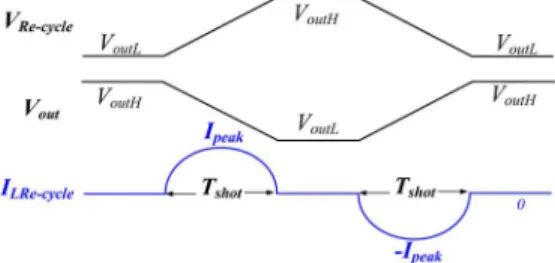
When the LED backlight module changes from G- or B-LEDs to R-LEDs, the signal is switched to low and the voltage will be decreased from high- and low-supplying voltage levels. In the meanwhile, the one-shot circuit will generate the signal to turn on the power transistor and decide the duration of the storing period. Therefore, the CR technique is ac-tivated and the extra charge on the output capacitor is delivered to the recycling capacitor via the inductor and power transistor . Owing to the current continuity of the inductor, the CR technique can continuously deliver extra charge to the recycling capacitor even that the output voltage is smaller than the voltage . Therefore, the high-sup-plying voltage level can be rapidly pulled down due to the charge storage on the recycling capacitor. Therefore, the CR technique can totally deliver the extra charge from the output capacitor to the external capacitor if the is chosen with a value similar to that of the . Therefore, the output voltage is rapidly pulled down to the lower regulation voltage for driving R-LEDs and the LED driver effectively stores the charge on the recycling capacitor . And the one-shot time is defined as (5) by the laws of conservation of charge:
(5) The difference voltage is defined as the difference between the high- and low-supplying voltage levels for controlling the charge storing or restoring procedure. is an av-erage inductor current in the charge storing procedure. There-fore, the period of CR technique is inversely proportional to the value of the inductor current according to (5). During the charge-recycling procedure, the peak value of inductor cur-rent is approximated to 2 and the slope of inductor current is defined as . In addition, the
Fig. 10. The timing diagram of the proposed charge-recycling technique.
value of is nearly equal to and the peak current ap-pears at time . Therefore, based on (5), the period of charge-recycling process can be derived as (6).
(6) According to (6), the value of is proportional to square of the product of the values of inductor and capacitor. It means the larger the values of inductor and capacitor need more storing/ restoring time. Furthermore, it is also important to limit the peak inductor current to prevent the circuit from being damaged by the large inductor current. Thus, the boundary of the peak cur-rent is expressed as (7).
(7) According to (6)–(7), the CR technique can utilize the larger inductor to decrease the peak inductor current and extend the period to accomplish the charge-recycling procedure. On other hand, when the one of the signals and is switched to low and the signals is switched to high, it means that the output voltage will be raised from low- to high-supplying voltage level for turning on the G-/B-LEDs. Therefore, the signal is generated by the one-shot circuit and the restoring period is started to restore the charge from the recycling capacitor to the output capacitor, thereby rapidly raising the output voltage back to its high-supplying voltage level. Hence, that means the restored charge can rapidly raise the output voltage back to it regulated voltage level and the rising recovery time is effectively decreased to extend the emission of the LED for ensuring the brightness. The timing di-agram of charge-recycling procedure is conceptually depicted in Fig. 10. Moreover, since the recycling voltage
switches between high- and low-supplying voltage levels, the body selection circuit is needed to avoid the forward biasing current for improving power efficiency.
The selection of the inductor and capacitor can ensure the CR technique smoothly transfers energy between two external capacitors depend on the equations (5)–(7). According to the previous designs, the pulling down response time depends on the load current and output capacitor. It is very hard to speed up the response time. However, due to the existence of the CR technique, the response time can be effectively reduced. Further-more, when the output voltage is needed to switch from
low- to high-supplying voltage level, the stored energy is re-stored back to the output capacitor . Considering another condition that G-LEDs changes to B-LEDs or vice versa, the CR technique is not activated due to the same output voltage level for driving G- or B-LEDs. The CR technique not only saves much power when the backlight module changes from G- or B-LEDs to R-LEDs but also speeds up the transient response time.
C. Reference Tracking Procedure
The FRT and CR techniques can speed up the transient re-sponse of tracking rere-sponse. Therefore, the reference tracking process of LED driver with mixed color sequential can be di-vided into four stages, which are described as follows.
1) Stage I: When the reference voltage steps from to , the peak value of the sawtooth current is in-creased instantly due to reference tracking mechanism. The cor-rection current , which is the output of amplifier, is also increased owing to a larger difference voltage between to . A feedforward current is determined by input voltage . The difference current between and is compared to the sawtooth current for determining duty cycle. Therefore, the current of is decreased instantly as a result that reference voltage is increased. Thus, by comparing and , the control signal is switched to a high level and the turn-on time of power transistor in Fig. 5 is lim-ited to a predefined maximum duty that represents a peak current level. Thus, the boost converter is controlled by the peak current loop. At this time, the CR technique also conveys the energy from the capacitor to output capacitor . There-fore, the voltage is decreased by CR technique and the output voltage can be quickly increased. The output voltage is raised to a high-supplying voltage level for a forward conduc-tion voltage of 6-series green or blue LEDs within a short time.
2) Stage II: When the output voltage approaches the high-supplying voltage level , the correction current is gradually decrease because the difference voltage between and is decreased and the characteristic of fast response of the amplifier [22], [23]. Hence, the current of is increased rapidly and then the outputs of the PWM generator can substitute for the peak current control to regulate the output voltage of the LED driver. Certainly, the static error is mini-mized due to the insertion of feedforward current com-pared to the current-mode boost converter with current-domain control.
3) Stage III: When the reference voltage is decreased instantly from to , the correction current by the amplifier is instantly decreased owing to a larger difference voltage between and . Furthermore, due to the reference tracking mechanism, the peak value of the sawtooth current is decreased instantly. Thus, the current is decreased and the value of is increased instantly as well. By comparing the values of and , the control signal can be adjusted to a lowest level to turn off power transistor illus-trated in Fig. 6. In addition, the CR technique is activated and stores extra energy on the capacitor at this time. There-fore, the output voltage of proposed LED driver is decreased according to load current and the CR technique. And the down
Fig. 11. The timing diagram of the proposed charge-recycling technique.
tracking can be quickly achieved compared to conventional con-verter after the implementation of the CR technique.
4) Stage IV: When the output voltage is decreased to the
low-supplying voltage level , the correction current is gradually increased. Due to the fast response of the ampli-fier, the current of is decreased instantly. The fast and stable pulse width control is guaranteed and the timing diagram of the up- and down-reference tracking response is shown in Fig. 11.
D. The Stability of the LED Driver With the FRT and CR Techniques
After the description of the FRT and CR techniques, the sta-bility of the whole system must be guaranteed to ensure the stable operation. Because the CR technique is enabled in the transient time of reference tracking procedure, the stability anal-ysis of LED driver can ignore the effect from the CR technique. Since the design of the LED driver is based on the voltage-mode boost converter design, the LED driver with FRT techniques is needed to be analyzed and compensated. The transfer function of a voltage-mode boost converter in CCM [24]–[26] is defined as (8).
where
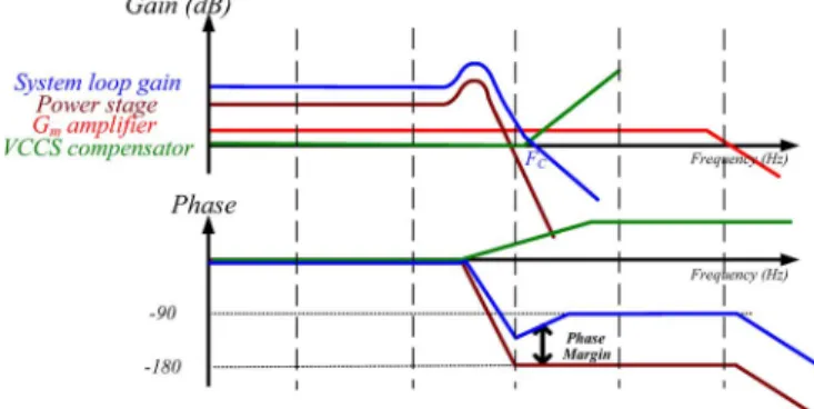
(8) is feedback resistor ratio defined by (3). is the amplitude of the sawtooth signal. is the double poles due to the output LC filter. The parameter is called the quality factor. is the right-half plane (RHP) zero of the boost converter in CCM op-eration. is the output equivalent load resistance. Instead of the error amplifier, the FRT technique uses the low-gain and high-bandwidth amplifier to speed up the reference tracking time. is used to stand for the transfer function of the amplifier and can be treated as a low-gain amplifier with having a high-frequency pole. As illustrated in Fig. 6(a), in order to
Fig. 12. The Bode plot of the proposed boost converter.
stabilize the whole system, a left-half plane (LHP) zero is in-serted by the voltage-control current source (VCCS) compen-sator [27], [28] to enhance the phase margin. Then, the system transfer function of the proposed structure is modified as (9).
where
(9) is an low-frequency LHP zero generated by the VCCS compensator. The parameter is the amplified factor of the compensation capacitor and is determined by the VCCS compensator. The stability of the proposed boost converter can easily promised by using a amplifier with a high-frequency pole above the crossover frequency and a low-frequency zero . The Bode plot of the converter as illustrated in Fig. 12 show the adequate phase margin [29]. Therefore, the phase of the boost converter was approximately 45 degrees to ensure the stability of the system.
III. CIRCUITIMPLEMENTATION
A. The Design of the Voltage Control Current Source Compensator
The purpose of the voltage control current source (VCCS) compensator is to generate a low-frequency zero to extend phase margin. The design of the VCCS compensator is depicted in Fig. 13. Due to the variations of the output voltage, the small-signal current can be expressed as (10) by using small inte-grated capacitors and . In addition, the resistors and must be used to reduce the DC level of output voltage for avoiding that the capacitor is damaged by higher voltage.
(10) is output impedance seen at node . The value of is low enough to be ignored since there is a negative feedback loop that is composed of transistors and [28]. Ideally, the small-signal current flows through transistor because the
Fig. 13. The circuit of the VCCS compensator.
impedance at the source of transistor is much smaller than that of the bias current source. Thus, the small-signal voltage at node is equal to (11).
(11) is the output resistance seen at node . In order to convert the small-signal voltage to current signal, a transconductance amplifier is used and thus the output current of the VCCS circuit is defined as (12).
(12) where is the multiplication factor to amplify the effective value of the small compensation capac-itor . That is only a small capacitor is needed to generate a LHP zero near the crossover frequency. Besides, the other para-sitic poles in the VCCS compensator locate at higher frequency because the value of impedance is small. Therefore, these poles have no effect on the stability of the system. Therefore, a low-frequency zero is generated by the VCCS circuit without inserting any low-frequency pole.
B. The Implementation of the PWM Generator With FRT Technique
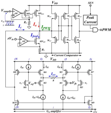
The circuit implementation of the PWM generator with FRT technique is shown in Fig. 14. The circuit is used to generate the prediction PWM control signal and consists of two voltage-to-current circuits, a amplifier, and a current comparator. In order to have the same transconductance of the two voltage-to-current converters, the resistors and of the two voltage-to-current converters are designed to have the same value. The upper bond of the voltage is defined as and the low bond of the voltage is defined as ground. Therefore, the voltages and are converted into current signals and to implement the equations (2)–(4) by the two voltage-to-current converters with the same transconductance. The matching methods of layout technique are carefully used to reduce the process variation between the two resistors. The amplifier [22] is used to convert the difference voltage between and to a
Fig. 14. The PWM generator with FRT technique consists of voltage-to-current converters,G amplifier, and current comparator.
current signal . That is the signals and are applied to the gates of transistor and , respectively. The output current is injected to the input of the current comparator. The flipped-voltage-follower (FVF) is used to minimize the resistance seen at node and for improving the linearity of the transconductance of the amplifier. Obviously, the reduction of the impedance at node or can be found as (13).
(13) Therefore, the transconductance of the amplifier is approx-imated to due to the low impedance at node and . After the operation of the three current mirrors, which are , , and , the correction current is defined as (14).
(14) The current is the summation of the ramp current , the feedforward current , and the correction current at the input of the current comparator. Thereby, the value of the current decides the duty of the PWM signal. Moreover, not only the prediction duty cycle can be decided by and but also the correction current can adjust the duty cycle to regulate the output voltage.
C. The Proposed One-Shot Generator for Charge Recycling Technique
The FCS algorithm implemented by FPGA send the control-ling signals ( , , and ) to turn on/off the different color LEDs in sequence as shown in Fig. 1. In addition, the LED driver not only supplies 16 V to supply 6-series R-LEDs but also supplies 21 V to 6-series G- or B-LEDs for minimizing the
Fig. 15. The timing diagram of modifier FCS signal in Section I of the notebook and the one shot signalT .
voltage across the current balance circuit to maintain high effi-ciency [8], [9]. According to the color of the backlight module in Section III of the notebook with FCS algorithm as illustrated in Fig. 3, the controlling signals , , and are turned on/off in sequence and can define the output voltage level as de-picted in Fig. 15. The black (K) frame means that all the LEDs are turned off to reduce the effect of color breakup. Furthermore, the output voltage is kept constant when the black frame is in-serted to the FCS algorithm. Until one of the controlling sig-nals which need different output voltage level is switched to the low level, the output voltage will be changed to the appreciate voltage for reducing power consumption on the current balance circuit. Therefore, when the output voltage switches from high-to low-supplying voltage level or low- high-to high-supplying voltage level, the LED driver will start the CR technique to transmit the charge for speeding the reference tracking procedure.
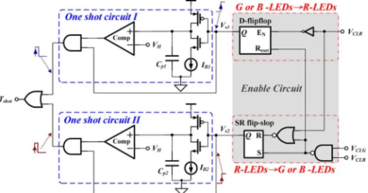
These signals ( , , and ) used to generate the one-shot signal are shown in Fig. 15 to decide the turning on/off the power transistor of the CR technique in Fig. 9. Therefore, the one-shot generator, which is composed of the en-able circuit and two one-shot circuits, utilizes the three signals ( , , and ) to start the CR technique as shown in Fig. 16. The enable circuit uses three input signals ( , , and ) to generate two signals and . The one-shot circuit produces the one-shot signal when one of the sig-nals and is instantly pulled to high. Furthermore, the one-shot circuit I will be reset until the signal is switched to low and so does the one-shot circuit II. When the LEDs backlight module turns off the G- and B-LEDs, the controlling signals and reset the signal to low. Therefore, when the signal is switched from high to low means that the R-LEDs will be turned on, the signal will be instantly pulled to high and the output voltage should change from high-to low-supplying voltage level. Therefore, when the signal is pulled to high, the capacitor is discharged by biasing cur-rent to generate the one-shot signal . Therefore, the signal is utilized to turn on the power transistor in Fig. 9 and thereby the CR technique is activated to store the energy on the recycling capacitor . The length of the one-shot signal can be calculated as (15).
(15) Therefore, the one shot circuit can modulate the length of one-shot time by adjusting the capacitor and biasing current for achieving the preferable CR technique. In practice, the length
Fig. 16. The circuit of the one shot generator.
Fig. 17. The current balance circuit.
of the one-shot time may be varied by the process variation. The value of the capacitor is trimmed to finely adjust the value of switching frequency [30]. Similarly, when the R-LEDs are turned off by the controlling signal , the SR-latch will reset the signal to low. Until one of the signals and is pulled to low, the signal will be switched to high and it repre-sents that the LED driver should supply high-supplying voltage level to turn on the G- or B-LEDs. Therefore, the signal will en-able the one-shot circuit to start the CR technique to restore the energy back to the capacitor . Thus, the CR technique can achieve the fast up- and down-reference tracking procedure and high efficiency without consuming much power.
D. Proposed Current Balance Circuit
In general, the light luminance of LEDs is controlled by the driving current [8], [9]. Therefore, the LEDs backlight module utilizes the current balance circuit to control the amount of driving current for regulating the constant light luminance of LEDs. The current balance circuit composed of three current generators is controlled by the signals , , , and from the FPGA as shown in Fig. 17. The current generator utilizes the operation amplifier (OP) and the resistor to op-erate as a voltage-to-current converter. Furthermore, the input signals , which is converted by the digital-to-analog (D/A) converter in the FPGA, determines the value of the driving current in the series connection LEDs. Thus, the voltage signal is used to generate the constant current. After the two current mirrors pairs, which are , , the current can be used to drive the 4 brunches of LEDs and thus the variation of drain-source voltage of these transistors will not have large influence on the value of current . Moreover, the FPGA uses the three signals , , and to turn on/off the R-, G-, and B-LEDs for achieving the FCS algorithm as shown in Fig. 3. Using the R-LEDs as an example, the transistor operates
Fig. 18. The chip micrograph.
Fig. 19. The module of RGB LED backlight driver for color filterless panel display.
in the cut-off region when the signal is pulled to high level. Thus, the current is equal to zero and unable to drive the R-LEDs. In other words, when the is pulled to low and the transistor operates in cut-off region, the voltage-to-current converter will start to convert the reference voltage to current signal for driving the R-LEDs. Therefore, the current balance circuit is used to generate the constant current to drive the LEDs for constant light luminance. The FCS algorithm can be achieved by turning on/off the LEDs according the values of signals , , and . When the current generator is activated to convert the current, the transistors operated in the saturation region generally stress the drain-source voltage for reducing the power consumption.
IV. MEASUREDRESULTS
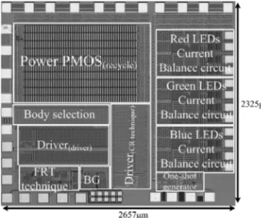
The proposed LEDs driver with CR and FRT techniques was fabricated in 0.25 m TSMC BCD 40 V technology and the mi-crograph of the chip is shown in Fig. 18. The RGB LED back-light module composed of LED driver with the FRT and CR techniques is depicted in Fig. 19 for 15.4’ LCD panel of the notebook.
Fig. 20(a) shows the one DC-DC converter without the ref-erence tracking technique supply only high-supplying voltage level as 21 V to drive all of the R-, G-, and B-LEDs. However, when the backlight module drives the R-LEDs by such high sup-plying voltage level, the voltage across the current balance cir-cuit is larger than that during driving the G-/B-LEDs. Therefore, the efficiency of the LED backlight module is deteriorated. The LEDs driver with the FRT technique can speed the transient per-formance of reference tracking, and thereby reducing the power dissipation. However, the up-reference tracking procedure can
Fig. 20. (a) The waveforms of the LED driver without reference tracking tech-nique. (b) The waveforms of the LED driver with the FRT Techtech-nique.
Fig. 21. The waveforms of the LED driver with or without the FRT and CR techniques.
be quickly achieved due to the FRT technique and the down-ref-erence tracking depends on the output capacitor and load cur-rent. Unfortunately, when the value of the load current is small, the output voltage is slowly decreased by the small load cur-rent as shown in Fig. 20(b), which shows the signal de-cides the turning on/off of the R-LEDs. The low value of the signal means the output voltage needs to be low-supplying voltage level as 16 V. On other hand, the high value of the signal means the output voltage needs to be high-supplying voltage level as 21 V. Therefore, when the LED driver operates at light loads, large output voltage across the current balance cir-cuit causes much power dissipated in the current balance circir-cuit. Certainly, the extra energy is always dissipated on the current balance circuit at any load condition. Therefore, the proposed CR technique will reduce the power consumption on the current balance circuit and increase the efficiency of the LED driver. The waveforms of LED driver with CR and FRT techniques can effectively speed the up- and down- reference tracking proce-dures as shown in Fig. 21. Therefore, the CR technique can save much extra energy on the recycling capacitor and the detail waveform of CR and FRT techniques is shown in Fig. 22. When the output voltage changes from high-supplying voltage level for G- or B-LEDs to low-supplying voltage level for R-LEDs, the one-shot generator sends the signal to turn on the power transistor for transmitting energy
Fig. 22. (a) WhenV changes from 1.1 V for G- or B-LEDs to 0.8 V for R-LEDs, the extra energy is stored in the auxiliary inductorL and ca-pacitorC , which is triggered by the one-shot generator. (b) WhenV changes from 0.8 V for R-LEDs to 1.1 V for G- or B-LEDs, the extra energy stored in the auxiliary inductorL and capacitorC is released to the output nodeV , which is also triggered by the one-shot generator.
from to . The duration of the signal is approximated to 7 s as shown in Fig. 22(a). Simultaneously, the transmits energy from the output capacitor to the recycling capacitor at time . Thus, the output voltage can be rapidly decreased from 21 V to 17 V within time . The value of about 7 s is faster than other con-ventional structure. Furthermore, the recycling voltage
is also raised from 17 V to 21 V because the extra charge is high efficiency to store on recycling capacitor . Thus, the fast response from high- to low-supplying voltage level is demanded for achieving high performance of the FCS algo-rithm. And then the settling time depends on the value of the output capacitor and load current. The output voltage is pulled down to near 17 V after the period . This voltage level is enough to drive the 6 series R-LEDs with minimized power loss since the voltage stress across the current balance unit is smaller that of the high supplying level as 21 V. But the CR technique also dissipates power due to the conduction loss. However, the efficiency still can be improved due to low conduction loss during the short storing/restoring time. When the low-supplying voltage level steps to high-supplying voltage
Fig. 23. Load regulation when load current changes from 80 mA to 240 mA.
level, the signal is sent to transferred the recycling energy on the back to the output capacitor for rapidly raising the output voltage to the regulated voltage. Thus, Fig. 22(b) shows the reversing current from
to at time . The output voltage gets stored energy from the CR technique of the LED driver at time about 7 s. Thus, the extra energy stored on the recycling capacitor is efficiently used to speed the up-reference tracking procedure. After the period , the FRT technique is used to regulate the output voltage to the high-supplying voltage level, which is 21 V, within time .
The load regulation is shown in Fig. 23, the value of load regulation is 0.5 mV/mA when input voltage is 12 V and the output voltage is 21 V. The load transient time is only 10 s when variation of load current is about 80 mA. It is ab-vious to find that the load regulation is improved [21] and the transient response time is short due to the FRT technique. The line regulation is shown in Fig. 24, the value of line regulation is 1.36 mV/V when the output voltage is 21 V and load current is 100 mA. Similarly, the recovery time of the line transient response is decreased within 10 s. For a conventional boost converter design with PI compensation, it is very hard to decrease the line/load transient response time within 10 s. Fig. 25 shows comparison of the power consumption between LEDs driver with or without CR and FRT technique. The LED driver without FRT and CR techniques always supplies 21 V and thereby the power still waste on the current balance circuit when the backlight module turn on the R-LEDs. However, the driver with FRT technique can reduce the power loss due to the small voltage across the current balance circuit. Furthermore, the proposed driver with FRT and CR techniques can reduce the power consumption and efficiently enhance reference tracking performance. When the RGB LED backlight module with FCS algorithm drives 12-branches LEDs and each branch consumes 20 mA, the LED driver without FRT and CR techniques con-sumes 1.04 W. However, the LED driver with the FRT and CR techniques switches different voltage level and consumes only
TABLE I PERFORMANCESUMMARY
Fig. 24. Line regulation when input voltage changes from 8 V to 13.5 V and back to 8 V when load current is 80 mA.
Fig. 25. Measured power loss of the LED driver with or without the FRT and CR techniques.
0.252 W. The power saving can achieve 0.788 W if the LED driver utilizes the proposed CR and FRT techniques. In addi-tion, when the LED driver drives the one branch of the LED array, the current balance circuit consumes a little power. That is, the difference power consumption with or without CR and FRT technique is smaller than that of driving many branches of the LED array. The reason is the quiescent current of the LED driver dominates most of the power loss in driving one branch of the LED array. However, after the implementation of the CR and
Fig. 26. (a) The power consumption of LCD panel with color filter and CCFL backlight is larger than 5 W. (b) The power consumption of the color filterless LCD panel with the proposed RGB backlight driver is about 2-3 W.
FRT techniques, the power consumption on the current balance circuit still can be reduced. Furthermore, the transient response is also speeded up due to the restored charge by the CR tech-nique. The performance summary is listed in Table I. Fig. 26(b) shows a notebook computer’s 15.4’ LCD panel is divided into three sections for the implementation of the FCS algorithm in Fig. 3. The color gamut is enhanced and the power consump-tion is reduced compared to the implementaconsump-tion with the CCFL backlight module as shown in Fig. 26(a).
V. CONCLUSION
An RGB LED backlight driver is proposed for rapidly switching between driving 6-series R- (about 16 V) and 6-series G-/B-LEDs (about 21 V). Owing to voltage difference about 5 V between driving series R- and series G-/B-LEDs, the FRT technique is presented to enhance line and load reg-ulations. Besides, the CR technique stores extra energy on the recycling capacitor at the transition from high-supplying voltage (21 V) to low-supplying voltage (16 V). On other hand, it can restore the energy back to output node to speed up the raising of voltage back to 21 V at the stage of driving G-/B-LEDs. Both the transient response time and efficiency are enhanced. The proposed LED driver with the FRT and CR techniques was implemented in 0.25 m TSMC BCD 40 V technology. Experimental results show that the load transition time can be reduced within 10 s and the line transient response time can be reduced within 10 s. It demonstrates the fast ref-erence tracking performance achieved by the proposed FRT technique. The power consumption of the backlight module in the implementation of the FCS algorithm is smaller than 3 W. Furthermore, the power loss due to the LED driver can be effectively reduced to about 24% of the LED driver without CR and FRT techniques. The proposed LED driver with the
[2] T. Shirai, S. Shimizukawa, T. Shiga, S. Mikoshiba, and K. Kalantar, “RGB-LED backlights for LCD-TVs with 0D, 1D, and 2D adaptive dimming,” in Soc. Inform. Display Dig. 44.4, 2006, pp. 1520–1523. [3] K. Käläntär, T. Kishimoto, K. Sekiya, T. Miyashita, and T. Uchida,
“Spatio-temporal scanning backlight for color-field sequential op-tically compensated bend liquid-crystal display,” in Soc. Inform.
Display Dig. 36.3, 2005, pp. 1316–1319.
[4] A. Yohso and K. Ukai, “How color break-up occurs in the human visual system: Mechanism of color break-up phenomenon,” in Soc. Inform.
Display Dig. 25.2, 2006, pp. 1223–1228.
[5] R. V. Dijk and J. A. Shimizu, “A system and method for motion com-pensation image planes in color sequential displays,” U.S. 6,831,948, Dec. 14, 2004.
[6] Datasheet “3508 White SMD LED,” Light House Technology Co., Ltd. .
[7] Datasheet “MAX16807/MAX16808: Integrated 8-Channel LED Drivers with Switch-Mode Boost and SEPIC Controller,” Maxim Integrated Products, Inc..
[8] O. Ronat, P. Green, and S. Ragona, “Accurate current control to drive high power LED strings,” in Proc. IEEE Applied Power Electronics
Conf., 2006, pp. 376–380.
[9] M. Doshi and R. Zane, “Digital architecture for driving large LED ar-rays with dynamic bus voltage regulation and phase shifted PWM,” in
Proc. IEEE Applied Power Electronics Conf., 2007, pp. 287–393.
[10] Datasheet “1206 RGB SMD LED” Light House Technology Co., Ltd.. [11] S. M. Baddela and D. S. Zinger, “Parallel connected LEDs operated at high frequency to improve current sharing,” IEEE Industrial
Applica-tion Soc., vol. 3, pp. 1677–1681, 2004.
[12] I.-H. Oh, “A single-stage power converter for a large screen LCD back-lighting,” in Proc. IEEE Applied Power Electronics Conf., 2006, pp. 1058–1063.
[13] C.-C. Chen, C.-Y. Wu, and T.-F. Wu, “LED back-light driving system for LCD panels,” in Proc. IEEE Applied Power Electronics Conf., 2006, pp. 381–385.
[14] H.-J. Chiu and S.-J. Cheng, “LED backlight driving system for large-scale LCD panels,” IEEE Trans. Ind. Electron., vol. 54, pp. 2751–2760, Oct. 2007.
[15] H. van der Broect, G. Sauerlander, and M. Went, “Power driver topolo-gies and control schemes for LEDs,” in Proc. IEEE Applied Power
Electronics Conf., 2007, pp. 1319–1325.
[16] M. Siu, P. K. T. Mok, K. N. Leung, Y.-H. Lam, and W.-H. Ki, “A voltage-mode PWM buck regulator with end-point prediction,” IEEE
Trans. Circuits Syst. II, vol. 53, no. 4, pp. 294–298, Apr. 2006.
[17] C.-Y. Hsieh, S.-J. Wang, Y.-H. Lee, and K.-H. Chen, “LED drivers with PPD compensation for achieving fast transient response,” in Proc.
IEEE Int. Symp. Circuits and Systems, 2008, pp. 2202–2205.
[18] M. D. Mulligan, B. Broach, and T. H. Lee, “A 3 MHz low-voltage buck converter with improved light load efficiency,” in IEEE
Solid-State Circuits Conf. Dig., 2007, pp. 528–529.
[19] C.-Y. Hsieh and K.-H. Chen, “Boost DC-DC converter with charge-re-cycling (CR) and fast reference tracking (FRT) techniques for high-ef-ficiency and low-cost LED driver,” in Proc. European Solid-State
Cir-cuits Conf. (ESSCIRC), Sep. 2008, pp. 358–361.
[20] H.-W. Huang, K.-H. Chen, and S.-Y. Kuo, “Dithering skip modula-tion, width and dead time controllers in highly efficient DC-DC con-verters for system-on-chip applications,” IEEE J. Solid-State Circuits, pp. 2451–2465, Nov. 2007.
Syst. II, pp. 1150–1154, Dec. 2007.
[24] K.-H. Chen, C.-J. Chang, and T.-H. Liu, “Bidirectional current-mode capacitor multipliers for on-chip compensation,” IEEE Trans. Power
Electron., pp. 180–188, Jan. 2008.
[25] R. W. Erickson and D. Maksimovic, Fundamentals of Power
Elec-tronics, 2nd ed. Norwell, MA: Kluwer, 2000.
[26] W. H. Ki, “Signal flow graph in loop gain analysis of DC-DC PWM CCM switching converters,” IEEE Trans. Circuits Syst. I, vol. 45, pp. 644–655, Jul. 1998.
[27] C. K. Chava and J. Silva-Martínes, “A frequency compensation scheme for LDO voltage regulators,” IEEE Trans. Circuits Syst. I, vol. 51, pp. 1041–1050, Jun. 2004.
[28] Q. Bian, Z. Yan, Y. Zhao, and S. Yue, “Analysis and design of voltage controlled current source for LDO frequency compensation,” in Proc.
IEEE Conf. Electron Devices and Solid-State Circuits, 2005, pp.
363–366.
[29] H.-W. Huang, C.-Y. Hsieh, K.-H. Chen, and S.-Y. Kuo, “Adaptive frequency control technique for enhancing transient performance of DC-DC converters,” in Proc. European Solid-State Circuits Conf.
(ES-SCIRC), Sep. 2007, pp. 174–177.
[30] H.-W. Huang, C.-Y. Hsieh, K.-H. Chen, and S.-Y. Kuo, “A 1 V 16.9 ppm/ C 250 nA switched-capacitor CMOS voltage reference,” in IEEE
Solid-State Circuits Conf. Dig., 2008, pp. 438–439.
Chun-Yu Hsieh was born in Taichung, Taiwan. He
received the B.S. degree in electrical and control engineering from National Chiao Tung University, Taiwan, in 2004, where he is currently pursuing the Ph.D. degree in electrical and control engineering.
His research area includes many projects of LED driver ICs and power management ICs at the Low Power Mixed Signal Lab. His interests include power management circuit designs, LED driver ICs, and analog integrated circuit designs.
Ke-Horng Chen (M’04–SM’09) received the B.S.,
M.S., and Ph.D. degrees in electrical engineering from National Taiwan University, Taipei, Taiwan, in 1994, 1996, and 2003, respectively.
From 1996 to 1998, he was a part-time IC De-signer at Philips, Taipei. From 1998 to 2000, he was an Application Engineer at Avanti, Ltd., Taiwan. From 2000 to 2003, he was a Project Manager at ACARD, Ltd., where he was engaged in designing power management ICs. He is currently an Associate Professor in the Department of Electrical Engi-neering, National Chiao Tung University, Hsinchu, Taiwan, where he organized the Mixed-Signal and Power Management IC Laboratory. He is an author or coauthor of more than 80 papers published in journals and conferences, and also holds several patents. His current research interests include power management ICs, mixed-signal circuit designs, display algorithm and driver designs of liquid crystal display (LCD) TV, red, green, and blue (RGB) color sequential backlight designs for optically compensated bend (OCB) panels, and low-voltage circuit designs.