PERGAMON
Microelectronics Reliability 40 (2000) 1491-1495RELIABILITY
www.elsevier.com/locate/microrel
Reliability of Passivated P-type Polycrystalline Silicon Thin Film
Transistors
D.Z. Peng a,*
,P.S. Shin a, T.C. Chang b
,C.Y. Chang
alnstitute o~f Eleetronies, National Chiao Tung University, Taiwan
bDepartment of Physics, National Sun Yat-Sen University, Taiwan
A b s t r a c t
We have used NH3, N20 and N2 to passivate the traps in the grain boundaries of the p-type polycrystalline silicon thin film transistors (p-type poly-Si TFTs). Two different stress conditions, drain voltage Vd o f - I 5V and -30V, have been applied to the poly-Si TFTs respectively while the gate voltage Vg were kept at -15V for both conditions and the stress time were 10 minutes at room temperature for all samples. The comparisons of I-V characteristics after stress with and without plasma passivations have been made, and the results indicated that the reliability will become worse for poly-Si TFTs after plasma passivations. © 2000 Elsevier Science Ltd. All rights reserved.
I. I n t r o d u c t i o n
Polycrystalline silicon thin film transistors are of interests for their widely applications in active matrix liquid crystal displays (AMLCDs)[1] and some memory devices such as dynamic random access memories (DRAMs)[2]. In order to obtain better device performance, plasma passivation is usually used to passivate the traps in the grain boundaries[3]. It is known that H2 plasma treatment will lead to tie up the hydrogen with the grain boundary dangling bonds, and therefore dramatically promote the device performances.
Unfortunately, the hydrogen passivation suffer a poor hot-carrier endurance because of the weak Si- ll bond[4]. F. S. Wang et al. compared the H2 and the NH3 passivated n-type TFTs[5] and showed that H2 passivation resulted in a lower hot carrier endurance than NH3 passivation. On the other hand,
Y. S. Lee found that the hot carrier endurance of N2 plasma treatment is better than that of the NH 3 plasma treatment for n-type TFTs[6].
In this experiment, we have used NH3, N2, and N~O to passivate the traps in the grain boundaries of the p-type TFTs, and we have applied two different stress conditions to accelerate the degradation of device performance. The results showed that the passivated poly-Si TFTs suffer lower stress endurance than unpassivated poly-Si TFTs. The p-type poly-Si TFTs after NH3, N2, and N20 plasma passivation show little differences after the stress in this experiment which are not seen in the previous results[5,6] for n-type TFTs.
2. Experiments
2.1. Device fabrication
* Corresponding author.
Email address: [email protected]
0026-2714/00/$ - see front matter. © 2000 Elsevier Science Ltd. All rights reserved. PII: S0026-2714(00)00106-2
1492 D. Z Peng et al./ Microelectronics Reliability 40 (2000) i491-1495 A 500nm thermally grown silicon-dioxide
(SiO2) was used as the starting substrate. Undoped amorphous silicon (a-Si) layers of thickness 100nm were deposited by 10w pressure chemical vapor deposition (LPCVD) on the oxide by pyrolysis of disilane (SizH6) at 460 °C and the deposition pressure was 120 mTorr. The a-Si film was recrystallized to poly-Si film in N2 ambient for 24 hours by furnace annealing. The crystallized poly- Si was employed as the channel layer with the grain size of about 1 gm. After defining the active islands, a 40nm thick SiO2 was thermally grown by dry oxidation. Another 300nm poly-Si film film was deposited at 620°C in the LPCVD system and patterned to be the gates of the devices. The source, drain, and gate regions were implanted by Boron for p-channel TFTs. After ion implantation, these samples were annealed in N 2 ambient at 900°C to activate the dopants. A 200rim-thick passivation oxide was deposited by PECVD at 300°C. The contact holes were opened and a 500nm aluminum layer were deposited by thermal evaporation system. The aluminum layer was then patterned as the metal pad for measurement. Three different gas sources ofNH3, N20 and N2 were used to passivate the p-type poly-Si TFTs in the PECVD system at 300°C, and the passivation time was 2 hours. 2.2. Stress conditions
Two different stress conditions were employed to the p-type poly-Si TFTs both for as fabricated devices and the devices after plasma passivations. The stress time is 10 minutes at room temperature for all samples.
• Condition 1: V g = -15V and Vd = -15V, W/L=50gm/5 pm
• Condition 2: V g = -15V and Vd = -30V, W/L= 10Bm/51.tm
3. Result and discussion
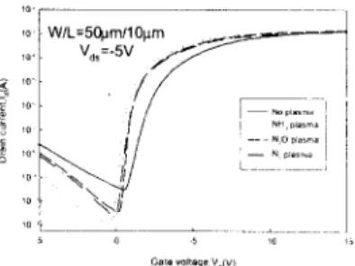
Fig. 1 compares the
Id-Vg
characteristics for as fabricated devices and those after plasma passivations of NH3, N20, and N2, respectively. It can be seen that after plasma treatment, the turn on current, subthreshold swing, threshold voltage and leakage current (V~,>0 for p-type TFTs) are significantly improved, which is attributed to the formation of Si-H and/or Si-N bonds in the poly-Si channel layer and Si/SiO2 interface after plasmapassivations[3,7], thereby reducing the dangling bonds and hence the trap state density (Nt) in the poly-Si layer and Si/SiO2 interface.
~.,
v d . = - 5 v ; / ' + ~
1o. f= ' ° ~
1o,i ... ,
- - N pI~o,o ]7
l o e 5 l o i s Gale ~ltage v#(v)Fig. 1 The transfer curves of drain current, ld versus the gate voltage, Vg for p-type TFTs with and without plasma treatment
Fig. 2~Fig. 5 show the
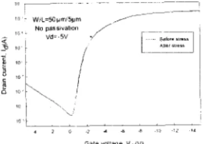
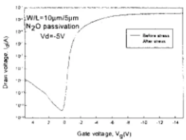
[d-Vg
characteristics before and after stress condition 1 for unpassivated devices, NH3, N20, and Nz passivated devices, respectively. From Fig. 2, we can find that the device without passivation shows little change except for the reduced leakage current, while from Fig. 3~ Fig. 5 for passivated TFTs, it can be seen that after stress, the performances become a little poor, ie.,subthreshold swing increases, threshold voltage shift and the field effect mobility degrades. However, the on/off current ratio, which is defined as the maximum current divided by the minimum current at Va=-5V, is increased because of the reduced leakage current. The degradations after stress condition 1 for passivated devices are almost the same in spite of their passivation sources, and the variations of some parameters after stress for unpassivated and passivated devices are listed in table 1. Note that the parameters were all characterized in linear region (Vd = -0. IV), except for the minimum drain current, which is calculated at Vd=-5V.Fig. 6-Fig. 9 show the Id-Vg characteristics before and after stress condition 2 for unpassivated, NH3, N20, and N2 passivated devices, respectively. The unpassivated poly-Si TFT after stress behaved like stress condtion l, ie., only reducing the leakage current. Fig. 7~Fig. 9 for passivated TFTs show, however, more severe degradations than those observed in stress condition 1, including the dramatic degradation of subthreshold swing and
large shift o f threshold voltage. In opposite to the stress condtion 1 for passivated devices, the on/off current ratio under stress condition 2 n o w reduced which is due to the increase o f the leakage current. The variations o f parameters are summarized in table 2. All parameters were extracted in linear region, except for Imm determined at Vd=-5V.
I n - W/L=SO #m/Spm No pas sivat~on .... / g i va=.sv 10 ! 2 0 -2 ~ I [ I ! 2 I 4 Gate voltage, Vg(V)
Fig. 2 The transfer curves of Id-Vg before and after stress condition 1 for unpassivated p-type poly-Si TFT
ie F . . . . lO, ~ W/L=S0prW5prn j ~ - - - - - - - lc ]. Vd= .5,./ / 6 ' ° ' i ~ t \ \ \ , , \ , , i ' 2 f 2 4 . 6 8 I U 12 14 Gate voltage, Vg(V)
Fig. 3 The transfer curves of Id-V~ before and after stress condition 1 for NH~ passivation
N20 p~ssivatlc.1 / ~ - - . . .
'°t
i"
g 1,,!
[ \ , L . . . . 2 ~) 2 6 ~ 10 1Z 14 Gate voltage Vg(V)Fig. 4 The transfer curves of Id-Vg before and after stress condition 1 for N20 passivation
,o W/L=50gm/5p~n ,o' N 2 passivation <" ~o Vd=-5V 6 0 Gale vogage, Vg(V)
Fig. 5 The transfer curves of Id-Vg before and after stress condition 1 for N2 passivated p-type poly-Si TFT
lO ~0 W/L=10p.m/S#rn / --- - - No passivation
/
,o Vd=-5V / 6 ' o ' ~ \ \ \ / / / lo ~ , . / 10 Gate voltage Vg(V)Fig. 6 The transfer curves Ofld-V g before and after stress condition 2 for unpassivated poly-Si TFT
'c [ W / L = 1 0 g m / 5 1 a m / ~ - ~ - - - ~
,c [NH3 passivation /
~ ~ Vd=-SV ,
. 2 0 -2 . ~ • IC, :~ ....
Gale voltage Vg(V)
Fig. 7 The transfer curves of ld-Vg before and after stress condition 2 for NH3 passivation
In table 1 the device performance without plasma treatment after stress condition I shows only a reduced o f f current, and those with plasma treatment after stress condition 1 have a little changes in addition to the reduced o f f current. One reason for this is that stress condition 1 causes electron traps in the oxide for the unpassivated device near the drain side[8], and both the electron trap in the oxide and breaking o f the Si-H, Si-N bonds in the poly-Si layer and/or poly-Si/SiO:
1494 D. Z Peng et al./ Microelectronics Reliability 40 (2000) 1491-1495 interface for the passivated ones, which can be seen
from the variations o f effective trap state density (NO extracted from slope of In [|d/(gg-Vfb)] VS (Vg- VI~,) 2 characteristic[9] as shown in Fig. 10 and Fig. 11 for unpassivated, NH3 passivated devices, respectively before and after stress condition 1. V~b denotes the flat band voltage.
io r . . . I ~ , ; W / L = l O p . m / f p m - - - .~.[,~O0a..,~.t,o~- _ _ ~ ,e, t } ,,,~ / g o, " ~ \ ! .~,,. '~;' 4 2 0 2 ~ ~ 8 ~0 12 t4 Gale voltage. Vg(Vj
Fig. 8 The transfer curves of Id-Vg before and after stress condition 2 for N20 passivated p-type poly-Si TFT
io . . . W / L : 1 0 # m / 5 ~ m ~ N 2 passivatior~ V d = - 5 V io, / ,o- I 1o, ~ j / 4 2 0 2 ~ ~ 8 io 12 ,4 Gate volta ge, Vg(V)
Fig. 9 The transfer curves of Id-Vg betbre and after stress condition 2 for N2 passivated p-type poly-Si TFT
The trapped electron in the oxide near the drain side will reduced the longitude electric field in the poly-Si film near drain when device is operated in the o f f state (Vg>0, VU<0), and therefore the off current is reduced for the unpassivated device[8]. As mentioned above, both trapped electron and breaking o f Si-H, Si-N bonds exist in the poly-Si layer and/or poly-Si/SiO2 interface, the dominant term is, however, the electron trap so that the off current is still reduced accompanied with a little change of the turn on characteristics for the passivated devices. In table 2 for the passivated devices, due to the large voltage applied to the gate and drain, the breaking of Si-H, Si-N was the dominant term under stress condition 2, resulting in increased donor-type trap state density[10], which can be verified in Fig. 12 with
large increase of Nt after stress condition 2. This is the consequence of the significant change of device performance• Nevertheless, unpassivated devices show little change as with those in stress condition t. The Si-H, Si-N bonds originally used to passivate the dangling bonds of poly-Si layer and/or poly-Si/SiO2 interface were broken again after the stress, so that the reliability of passivated device is an important issue for poly-Si TFTs.
Table 1
Variations of parameters after stress: Va=Vg=-I 5V. ¢z Ek, S.S , Imi> V,1 are the field effect mobility, subthreshold swing, minimum drain current and the threshold voltage, respectively.
Passivation A /-tel:/ A S . S / Almin/ 2~V,h(V) /2 ev S.S Imi n . . . 0.01 0.02 -0.53 0.02 NH 3 -0.05 0.26 -0.76 -0.38 N20 -0.02 0.26 -0.63 -0.34 N 2 -0.02 0.09 -0.62 -0.26 Table 2
Variations of parameters after stress: Vd=2Vg--30V. # Ev , S.S , lmin, Vth are the field effect mobility, subthreshold swing, minimum drain cunent and the threshold voltage, respectively.
Passivation ~ / z e v / /kS.S/ &Imm/ :~V,t,(V) LI- S . S I m i n . . . 0 - 0 -0.54 ~0 NH3 -0.18 0.85 3.25 -1.23 N20 -0.14 0.47 4.50 -1.15 N2 -0.16 1.00 14.40 - 1.09 , .. No passivation " . N t - 3 7 X 1 0 1 2 c m - 2 % " g . 8,lere S, . . . . ( V g V t ~ ) 2
Fig. 10 Slope of plot used to determine the value of trap state density, Nt for unpassivated TFT before and after stress condition 1.
V d V g - 1 5 V . . . . o N H 3 p a s s i v a t t o n o . . - >~ , , . N t - - N 1 - 2 7 5 X 1 0 1 2 cm - 2 e ~ f l ~ , S ~ r e ~ s ( V g - V f b ) -2
Fig. 11 Slope of plot used to determine the value of trap state density, N~ for NH 3 passivated TFT before and after stress condition 1.
before and after stress. Nevertheless, in addition to the electron traps, there are generations of N~ for passivated devices especially larger for higher drain stressed, and the ANt after stress condition 1 and 2 are 0.75x1012 cm -2 and 5.8x10 ~2 cm -2, respectively, for NH3 passivation. So we can conclude that after plasma passivation the p-type poly-Si TFTs show poorer reliability than unpassivated devices in spite of which one of the three passivation sources is chosen.
Referen ces V d - 2 V g - 3 0 V N H 3 p a ~ s i v a t l o n ,, N t - 2 9 X 1 0 1 2 c m "2 % N t - 7 8 X 1 0 1 2 cm~'2 a B e f o r e S t r ~ s ~ A f t e r S l f ~ s s (V g - V 1~o) "2
Fig. 12 Slope of plot used to determine the value of trap state density, Nt for NH3 passivated TFT before and after stress condition 2.
4. C o n c l u s i o n
Reliability of unpassivated, NH3, N20 and N 2 passivated p-type poly-Si TFTs was studied after two stress conditions. Under stress condition 1, Vg=Vd =-I5V, the unpassivated devices show almost no change with its turn on characteristics but with reduced leakage current, while for passivated devices there is a little change with its turn on curve in addition to the reduced leakage current. At stress condition 2, Vd=2Vg=-30V, the performance of passivated devices become poorer compared with that in stress condition 1, and the change of Id-Vg characteristics after stress condition 2 for unpassivated devces is the same as in stress condition 1.
The results indicate that there are electron traps in the gate oxide for unpassivated devices, the extracted Nt (~3.7x1012 cm 2) shows no difference
[1]
[2]
[3l
[4]
[5]
[6] [7][81
[91
[10] Rodder, M, IEEE Electron Device Lett, vol 118, pp. 346°348.
S. Morozumi, K. Oguchi, S. Yazawa, T. Kodaira, H. Ohshima, and T. Mano, SID Dig.,
1983, p. 156.
S. D. S. Malhi, H. Shichijo, S. K. Banerjee, R. sundaresan, M. Elahy, G. P. Polack, W. F. Richardson, A. H. Shah, L. R. Hite, R. H. Womack, P. K. Chatterjee, and H. W. Lain, IEEE Trans. Electron Devices, 1985, vol. 32, No. 2, pp. 258-281.
T, I. Kamins, and P. J. Marcoux, IEEE Electron Device Lett, 1980, vol. 1, p. 159
S. Banerjee, R. Sundaresan, H. Schichijo, and S. Malhi, IEEE Trans. Electron Devices, 1988, vol. 35, pp. 152-157
F. S. Wang, M. J. Tsai, and H. C. Cheng, IEEE Electron Device Lett., 1995, vol. 16, No. 11, pp. 503-505.
Y. S. Lee, H. Y. Lin, T. F. Lei, T. Y. Huang, T. C. Chang and C. Y. Chang, Jpn. J. Appl. Phys.,
1998., vol. 37, No. 7, pp. 3900-3903.
J. H. Kim, E. Y. Oh, B. C. Ahn, and D. Kim, Appl. Phys. Lett., 1994, vol. 64, No. 6, pp. 775-776.
J.Y. Lee, C.H. Han; C.K. Kim , Tech Dig IEDM, 1995, pp.523-526.
J. kevinson, F. R. Shepherd, P. J. Scanlon, W. D. Westwood, G. Este, and M. Ride, J. Appl. Phys, 1982, vol. 53, No. 2, pp. 1193-1202