國 立 交 通 大 學
應用化學研究所
博士論文
矽化鈦奈米結構之成長及其鑑定
Growth and Characterization of Titanium
Silicide Nanostructures
研 究 生:林煌凱
指導教授:裘性天 博士
李紫原 博士
Contents
Contents ... I
Abstract ... IV
Acknowledgments ... VIII
List of Tables ... X
List of Figures ... XI
Chapter 1 Introduction ... 1
1.1 Introduction ... 1
1.2 Metal Silcide ... 2
1.3 Titanium Silcide ... 4
1.3.1 Structure and Properties of Titanium Silicide ... 4
1.3.2 Synthesis of Titanium Silicide ... 6
1.4 Metal Silicide Nanowires ... 7
1.4.1 Synthetic Methods of Metal Silicide NWs ... 9
1.4.1.1 Silicidation of Si or Metal NWs ... 9
1.4.1.2 Deposition of Si Sources on Metal Films ... 10
1.4.1.3 Reaction between Metal Vapor Sources and Si
Substrates ... 10
1.4.1.4 Deposition of Metal and Si on the Substrates
Simultaneously ... 11
1.4.2 Applications of Metal Silicide NWs ... 13
1.5 Introduction of Electron Field Emission ... 15
1.6 Aim of This Thesis ... 18
Chapter 2 Ti
5Si
3Nanowire and Its Field Emission Property ... 27
2.1 Introduction ... 27
2.2 Experimental Section ... 28
2.2.1 Materials ... 28
2.2.2 Synthesis Procedure ... 28
2.2.3 Characterization Instruments ... 29
2.3 Results and Discussion ... 30
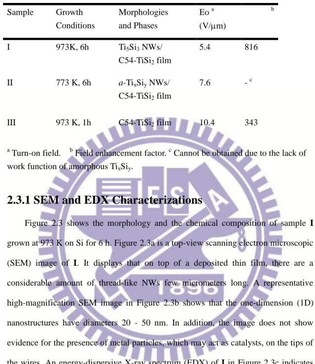
2.3.1 SEM and EDX Characterizations ... 31
2.3.2 XRD Characterizations ... 33
2.3.3 TEM Studies ... 33
2.3.4 Influence of the Growth Conditions for the Synthesis of
NWs ... 36
2.3.5 Proposed Reaction Pathway ... 37
2.4 Electron Field Emission Property Studies ... 38
2.5 Conclusions ... 40
2.6 References ... 41
Chapter 3 Chemical Vapor Deposition of TiSi Nanowires on C54 TiSi
2Thin Film – An Amorphous Titanium Silicide Interlayer Assisted
Nanowire Growth ... 44
3.1 Introduction ... 44
3.2 Experimental Section ... 48
3.2.1 Growth of Titanium Silicide Samples ... 48
3.2.2 Instruments for Characterizations ... 48
3.3 Results and Discussion ... 49
3.3.1 SEM and EDX Characterizations ... 50
3.3.3 TEM Studies of TiSi NWs ... 55
3.3.4 Characterization of the Interface between TiSi NWs and
C54 TiSi
2Film... 57
3.3.5 Growth Pathway of TiSi NWs ... 62
3.3.6 Electron Field Emission Properties of Titanium Silicide
Samples ... 67
3.4 Conclusions ... 69
3.5 References ... 70
Chapter 4 Chemical Vapor Deposition of Ti
xSi
yFilm and Single
Crystalline C49 TiSi
2Nanoplates ... 76
4.1 Introduction ... 76
4.2 Experimental Section ... 77
4.2.1 Synthesis Procedure ... 77
4.2.2 Characterization Instrument ... 77
4.3 Results and Discussion ... 78
4.3.1 Titanium Silicide Films Grown at Different Temperatures
... 79
4.3.2 Titanium Silicide Film Grown at Different Time ... 82
4.3.3 Synthesis of C49 TiSi
2Nanoplates ... 86
4.3.3.1 Characterization of the C49 TiSi
2Nanoplates ... 86
4.3.3.2 Proposed Reaction Pathway of the C49 TiSi
2Nanoplates ... 88
4.4 Conclusions ... 91
4.5 References ... 92
Chapter 5 Conclusions ... 94
Growth and Characterization of Titanium Silicide Nanostructures
Student: Huang-Kai Lin Advisor: Dr. Hsin-Tien Chiu
Dr. Chi-Young Lee
Institute of Applied Chemistry, National Chiao Tung University
Abstract
Recently, synthesis of various metal silicide nanowires (NWs) has raised many
attentions due to their excellent physical properties. In this work, we demonstrate the
synthesis of titanium silicide nanowires, nanoplates, and thin films via a unique
chemical vapor deposition process, using TiCl4 and Ti powder as the precursors,
without the usage of template and catalysts. Field emission properties, growth
mechanism of these titanium silicide samples were also investigated.
Titanium silicide NWs, including single crystalline Ti5Si3 NWs and crystalline
TiSi NWs, were prepared by reacting titanium subchlorides TiClx (x = 1-3), generated
by the reaction between TiCl4(g) and Ti metal in the high temperature zone at 1173 K
initially, and the Si substrates in the lower temperature zone at 723 - 1073 K. The
diameters of the nanowires are 20 - 80 nm, and the lengths are several micrometers.
The growth directions of the Ti5Si3 and TiSi NWs are determined to be along the [001]
and [010] axes, respectively. An amorphous titanium silicide interlayer was observed
between the NWs and the C54-TiSi2 film. This interlayer, probably existed as a
quasi-liquid thin film during the growth, appears to be the key factor to assist the NW
development.
The C49 TiSi2 nanoplates on Si substrate were obtained at a low TiCl4 vapor
pressure condition. The preferred basal plane of the C49-TiSi2 nanoplates was
crystal structure nature of the C49-TiSi2. The characterization and the growth
mechanism of the two-dimensional nanostructure will be discussed below. Comparing
with preferred growth direction the titanium silicide NWs, [001] and [010] for Ti5Si3
NWs and TiSi NWs, respectively. The crystal structure nature takes an important role
on the growth of anisotropic nanostructures.
The field emission properties of the titanium silicides samples have been studied.
The results show that the field emission performances are highly dependent on the
morphology and crystal structures of the NWs and thin films. The high aspect ratio
nature of the NWs has improved the performance of field emission properties. The
field emission property obtained from Ti5Si3 and TiSi NWs on C54 -TiSi2 thin film
demonstrates low turn-on fields Eo of 5.4 and 5.25 V/m and high field enhancement factor of 816 and 876, respectively. These remarkable results suggest that titanium silicide nanoemitters could serve as promising candidates for future field emission
矽化鈦奈米結構之成長及其鑑定
研究生: 林煌凱 指導教授: 裘性天 博士
李紫原 博士
國立交通大學應用化學所
摘 要
金屬矽化物奈米線具有低電阻、良好的熱穩定度等優異的特性。近年來,製 備各種金屬矽化物奈米線成為重要的研究議題。本研究中我們提出利用化學氣相 沉積法以四氯化鈦與鈦金屬為反應前驅物,並且在不使用模版或金屬催化劑的條 件下成長矽化鈦奈米線、二維奈米片狀產物及薄膜。此外本研究也對矽化鈦奈米 材料的成長機制以及電子場發射性質作了詳細的探討。 首先,我們利用在 1173 K 由四氯化鈦與鈦金屬生成的 TiClx (x=1-3)與在低 溫區 (723 – 1073 K) 的矽基材反應後可以得到各種矽化鈦奈米線。本研究中所 得矽化鈦奈米線具有兩種不同的結晶型態,分別為三矽化五鈦(Ti5Si3)以及矽化鈦 (TiSi)。矽化鈦奈米線的直徑分布大約為 20 – 80 奈米,線長可長達數個微米。 Ti5Si3及 TiSi 奈米線的成長方向經過鑑定分別為[001]以及[010]方向。在奈米線 以及其下方的矽化鈦薄膜之間可以觀察到一層非晶相矽化鈦薄膜,此半液相薄膜 在奈米線的成長裡扮演了相當重要的角色。 利用相同的反應,在 TiCl4前驅物的蒸氣壓於相對低的條件下,可以得到 C49 二矽化鈦二維奈米結構。經過分析,此二維結構傾向展露出(010)晶面,此一特 性源自 C49 二矽化鈦本身的層狀晶體結構。由此二矽化鈦二維奈米結構及前述 奈米線的結果可知本論文中提及奈米結構的非等向性成長與材料本身的晶體結 構排列有相當大的關聯。 經由探討矽化鈦樣品的電子場發射性質,顯示出樣品的形貌及結晶性與其場發射特性具相當的關聯性。可知矽化鈦奈米線具有很高長寬比使得其場發射特性
具有很好的表現。結果顯示 Ti5Si3與 TiSi 奈米線具有很低的起始電場 Eo 分別
為 5.4 與 5.25 V/m,以及優異的場增強因子 可達到 816 與 876。從研究結果
Acknowledgments
終於,也到了這一天,我要離開待了九年半的交大。當初懵懂的大一新生已 經要拿到博士學位。回想這些日子所遇到的人、發生的事,心中充滿了滿滿的溫 暖與感動。感謝這一路上給我支持、陪伴、幫助與鼓勵的每一個人。陪我ㄧ起渡 過這些辛苦忙碌卻又充實豐富的日子,並且順利地完成這本論文。 心中要感謝的人真的很多,首先感謝我的指導老師—裘性天老師以及李紫原 老師。我很幸運能夠有兩位指導老師,不論是學術研究、待人處世我從兩位老師 身上分別學到了很多。 從大一的普化課開始就感受到裘老師的風趣與幽默。大三的無機化學課更讓 學生訂下了日後研究的方向。進入實驗室後,老師以淵博的學識與無限的創意, 不斷的給予我深入的指導。裘老師給予我架設場發射機台以及出國參加研討會的 機會,這些經驗大大地開拓了學生的視野。在生活上,老師自由、親民的作風讓 我的研究生涯不那麼枯燥乏味,與老師的午餐約會總是羨煞其他的老師與學生 們,也讓學生學到了許多待人處世的道理。 由於實驗有很多部分在清大完成,再加上論文的主軸—矽化鈦的合成是接續 李老師之前的研究,與李老師的互動比其他交大的夥伴多了很多。很感謝老師一 直以來在實驗上細心與耐心的指導。此外,老師的愛心也讓學生感到十分敬佩, 老師兼具科技與人文氣質的風範更是學生學習的榜樣。真的非常感謝兩位老師一 路來的指導、照顧以及包容,這份恩情,學生會永遠銘記在心。 在此,也感謝論文口試委員陳登銘教授、李積琛教授、周立人教授、黃暄益 教授與吉凱明教授對此論文的批評與指導,使學生的論文更加完善。此外也特別 感謝李積琛老師在晶體結構與成長上的建議以及周立人老師在電子顯微鏡上的 支援。謝謝每一位老師的用心指導以及鼓勵。 感謝交大實驗室裡的每一位同伴,張裕煦學長對實驗認真嚴謹,對人風趣幽默的態度一直是我的模範。此外簡俊雄學長、王隆昇學長、Baken、黃志豪、小 黑與彭治偉學長在實驗上提供了很多的協助。亭凱、進興、高翔、宇婕、Sif、 嘉芳、Goby、昕君、大支、季勳、馨緯、最美麗的媽咪佳兒學姐、不需多說老室 友蕭蕭、搞笑又負責的昱良、可愛的亦諄、貼心又善良的 Wei Wei、悶騷的大銘、 帥氣的文志、有氣質的佑蕙、美食專家與籃球高手心安、手藝高超的 Kimi、康 樂股長奕廷、善良的小栗、人很好的凱捷、認真又細心的小童與鄒宗育。很高興 能夠與你們在同一個實驗室,讓我的研究生活多采多姿,也謝謝還在實驗室的大 家陪我渡過最後這一段日子。 清大實驗室裡的老人們鈺芬、正得、旻橋、奕仁以及聰盈。還記得當初大家 在材料中心一起奮鬥的光景,如今大家都已各奔前程。很感謝有你們的幫助與經 驗的分享,讓我成長了許多。弘麒、名輝、彥百、鑑嘉、博欽、婷婷與久萱也謝 謝你們陪我度過了很多充滿歡笑與汗水的時光。
此外,清大 TEM 的余宜真小姐,清大 ESCA 蔡靜雯小姐、交大 SEM 陳悅婷小
姐、陳聯珠小姐以及吳艾軒小姐,謝謝你們的幫助讓我能得到高品質的實驗數據。
謝謝 Sunny 這九年半來一直陪在我的身邊,鼓勵我、支持我。很高興能夠與
你分享生活中的所有喜怒哀樂,是你給我力量讓我能夠克服所有的艱難,此生有
你是我最幸福的事。最後要感謝我的父母與姊姊這些年來默默的支持,你們的付
List of Tables
Chapter 1
Table 1.1 Physical properties of some common used metal silicides. ... 3
Table 1.2 Crystal parameters and physical properties of the titanium
silicides. ... 4
Chapter 2
Table 2.1 Summary of Samples ... 31
Chapter 3
Table 3.1 Summary of Titanium Silicide Samples ... 47
Table 3.2 Assignments of the XRD Peaks in Figure 3.4 ... 54
List of Figures
Chapter 1
Figure 1.1 Binary phase diagram for Ti-Si system. ... 3
Figure 1.2 Crystal structures of the titanium silicides. (a) ab projection
and side view for Ti
5Si
3crystal structure, (b) bc projection for TiSi crystal
structure, (c) ab projection for C54 TiSi
2. ... 6
Figure 1.3 (a) Schematic diagram for silicide NWs synthesized by
Chemical vapor transport (CVT), (b) Synthesis of silicide NWs through
single source precursor chemical vapor deposition (CVD). ... 12
Figure 1.4 Energy diagram of metal-vacuum level (a) without electric
field, (b) under high electric field. ... 15
Chapter 2
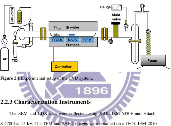
Figure 2.1 Experimental setup of the CVD system. ... 29
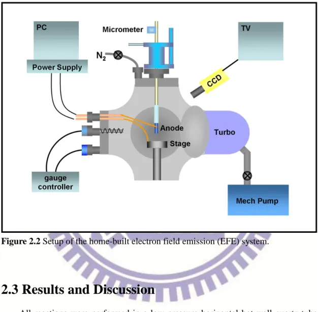
Figure 2.2 Setup of the home-built electron field emission (EFE) system.
... 30
Figure 2.3 SEM images of sample I grown on Si. (a) Top view, (b) high
magnification image, (c) EDX, and (d) side view image. ... 32
Figure 2.4 SEM images of II (a), (b) and III (c), (d) grown on Si. ... 32
Figure 2.5 XRD patterns of samples I, II, and III. ... 33
image, (b) SAED pattern of the sample in (a) showing a [1-10] zone axis,
(c) high-resolution image from the selected section in (a). ... 34
Figure 2.7 Auger depth profile of I. ... 35
Figure 2.8 (a) TEM image of NW isolate from sample II, (b) SAED
pattern showing that the NW is amorphous, (c) EDX of the selected area
in (a) indicates that the composition of the NW are Ti and Si. The NWs in
II could be designated as a-Ti
xSi
yNWs. ... 35
Figure 2.9 SEM images of samples grown at similar condition but
different precursors with sample I. (a) without the Ti metal, (b) without
the TiCl
4. ... 36
Figure 2.10 Proposed Growth Steps of Ti
5Si
3NWs. ... 38
Figure 2.11 Electron field emission current density as a function of
applied electric field of samples I – III. Inset shows their corresponding
Fowler-Nordheim plots. ... 39
Chapter 3
Figure 3.1 SEM images of I grown on Si. (a) Top-view and EDX (inset),
(b) high magnification image, (c) low magnification side-view, and (d)
high magnification side-view image. ... 50
Figure 3.2 SEM top-view and side-view (inset) of (a) II, (b) III, (c) IV,
Figure 3.3 XRD patterns of I - V. Assignment of peaks: spheres,
C54-TiSi
2; square: TiSi (020); diamond: Ti
5Si
3(002); triangle: Si (020),
this forbidden signal only appears in several samples grown on a specific
batch of Si substrates. For clarity, Si (400) at 69.2
ois not shown. ... 53
Figure 3.4 (a) Detailed XRD of I from 25
oto 38
o, (b) XRD of I from 20
oto 80
o(spheres, C54-TiSi
2; square: TiSi; triangles: Si), and (c) XRD of the
Si wafer used to grow silicides in samples I – III. 33.2
o: Si (200), 56.5
o:
Si (311), 69.5
o: Si (400), 61.7
oand 65.9
o: unable to assign. ... 54
Figure 3.5 (a) TEM image of a NW isolated from I, (b) SAED pattern
and (c) HRTEM image from the circled region in (a), and (d) TEM and
EDX elemental line profiles of another NW from I. ... 56
Figure 3.6 (a) TEM image of a NW isolated from I, (b) high
magnification image from (a), (c) SAED pattern from the circled region
in (a), and (d) HRTEM image of the squared area in (b). ... 56
Figure 3.7 (a) SEM side-view of I showing an interlayer between TiSi
NWs and a TiSi
2film, (b) enlarged view of (a), (c) SEM side-view of IV
showing a TiSi
2thin film, and (d) enlarged view of the rectangular region
in (c). ... 57
Figure 3.8 SEM EDX analyses of (a) I and (b) V. Chemical compositions
of the circled areas are listed below. ... 58
arrows mark the limits of the interlayers. ... 59
Figure 3.10 (a) Low-magnification cross-sectional TEM image of I
showing the presence of NWs on top of a thin film and (b)
high-magnification image of the dashed rectangular area in (a). ... 59
Figure 3.11 (a) Low-magnification cross-sectional TEM image of I
showing the presence of NWs on top of a thin film and (b)
high-magnification image of the dashed rectangular area in (a). ... 60
Figure 3.12 (a) Cross-sectional TEM image of the interface in I, (b)
HRTEM image and (c) SAED pattern from the solid square region in (a).
EDX spectra from (d) the solid and (e) the dotted circled areas in (a). The
Cu signal is from the Cu TEM grid. ... 61
Figure 3.13 HRTEM images of the selected crystallites shown in Figure
3.11d. Possible crystal plane assignments are designated in the images. . 62
Figure 3.14 Proposed growth pathway of the TiSi NWs. (x denotes
variables). ... 63
Figure 3.15 Crystal models of orthorhombic TiSi viewing along (a) a, (b)
b, and (c) c axes. The short Si-Si bonds (0.2171 nm) are linked in yellow
sticks. Orthorhombic TiSi (JCPDS 17-0424, ICSD 43494): space group
Figure 3.16 Crystal models of hexagonal Ti
5Si
3viewing along (a) a and
(b) c axes. Viewing along b axis is equivalent to viewing along a axis.
The short Ti-Ti bonds (0.25754 nm) are linked in yellow sticks.
Hexagonal Ti
5Si
3(JCPDS 78-1429, ICSD 62591): space group P6
3/mcm
(no. 193), a = 0.7610 nm, c = 0.51508 nm. ... 66
Figure 3.17 EFE current density as a function of applied electric field of
samples I, and III–V. Inset shows their corresponding Fowler-Nordheim
plots. ... 68
Chapter 4
Figure 4.1 Top-view and side-view SEM images of samples grown at
different reaction temperatures for 60 min. (a)-(b) 723 K (I), (c)-(d) 773
K (II), (e)-(f) 873 K (III), (g)-(h) 973 K (IV), and (i)-(j) 1023 K (V). ... 80
Figure 4.2 High-resolution XPS spectra of the film grown at 973 K for
60 min. (a) Ti 2p1/2 and Ti 2p3/2 electrons and (b) Si 2P electron... 81
Figure 4.3 XRD patterns of samples prepared at different temperatures
for 60 min (I-V). ... 82
Figure 4.4 ... 84
Figure 4.5 XRD patterns of samples synthesized at 973 K for different
time. ... 85
Figure 4.6 Characterization of sample IX, grown on Si wafer at 973 K
low magnification image, and EDX spectrum (inset), (b) high
magnification image of the nanoplates, (c) enlarged-view of the nanoplats,
and (d) XRD pattern. ... 87
Figure 4.7 TEM studies of sample IX. (a) Low-magnification TEM
image, (b) EDX spectrum, (c) SAED, and (d) HRTEM image were
obtained at the square area in (a). ... 88
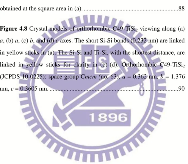
Figure 4.8 Crystal models of orthorhombic C49-TiSi
2viewing along (a)
a, (b) a, (c) b, and (d) c axes. The short Si-Si bonds (0.232 nm) are linked
in yellow sticks in (a). The Si-Si and Ti-Si, with the shortest distance, are
linked in yellow sticks for clarity in (b)-(d). Orthorhombic C49-TiSi
2(JCPDS 10-0225): space group Cmcm (no. 63), a = 0.362 nm, b = 1.376
Chapter 1
Introduction
1.1 Introduction
Transition metal silicides, intermetallic compounds between metals and silicon,
show unique and various physical and chemical properties that are important in both
scientific and engineering aspect, especially for Si based integrated circuit devices.1-4 Among the most studied silicides, such as silicides of Ti, Cr, Fe, Co, and Ni, titanium
silicides show high thermal stability, low electrical resistivity, low work function, and
low density.3,5,6 Thus, many efforts have been devoted to the researches about the application of titanium silicides.
Novel physical and chemical properties are often obtained when dimensions of
the materials are reduced to nanoscale. One-dimensional nanomaterials have attracted
tremendous amounts of attention for technological applications, such as sensors,7 laser devices,8 and electrical systems.9 An increasing effort has been devoted to fabricating nanomaterials for new field emitters, such as CNTs (carbon nanotubes),10 nano-diamond coated Si nanowires (NWs),11 SiC NWs and nanotubes,12,13 metal oxides14 and metal silicides. Recently, many studies about the fabrication of free standing silicide nanowires of Ti,15-24 V,25 Cr,26-29 Mn,30,31 Fe,32-35 Co,36-42 Ni,43-58 Ta,59-61 and Pt62-65 have been reported because of their superior properties and compatibility with Si based integrated circuit devices.Among them, titanium silicides
are potential candidates for building blocks for nanoelectronics and field emission
devices due to their relative low resistivity (10 – 60 Ω cm), high thermal stability, and low work function.3,5,6 For titanium silicide NWs, the fabrication of TiSi2
NWs,15,20,24 TiSi nanopins,16,17 and Ti5Si4 nanobats21 through various processing
techniques, including chemical vapor deposition (CVD) and physical vapor deposition
(PVD), have been demonstrated recently.
In this dissertation, we will reveal the growth of different kind of titanium
silicdes samples, including Ti5Si3 NWs, TiSi NWs, C49-TiSi2 nanoplates and titanium
silicides thin films (C49-TiSi2 and C54-TiSi2) via a unique CVD process.66
Microstructures, growth mechanism and and field emission properties of the titanium
silicdes NWs and thin films will be discussed in detail.
1.2 Metal Silcide
Metal silicides have attracted attention because their superior properties, such as
low and metal-like resistivities (cm – mcm) and high thermal stability, which could meet the requirements for modern Si-based electronic devices.3 The most studied silicdes are NiSi2, CoSi2, TiSi2, and FeSi2. NiSi2 has the best lattice mach to
silicon, CoSi2 and TiSi2 possessed low resistivities and often used in the electronics
devices. FeSi2 is a direct energy gap semiconductor with a small gap of 0.87 eV. The
physical properties of the most used metal silicides are listed in Table 1.1. The
applications of metal silcides are summarized as below: (1) diffusion barrier,67-69 (2) ohmic contact and interconnect,70,71 (3) Schottky diode,71 (4) polycide gate,72,73 (5) multilevel metallization,74,75 (6) shallow silicide contact,69 (7) epitaxial silicides,76-78 (8) thermoelectric material,79,80 and (9) photovoltaic application.81 Besides, for many metal silicides, varying the synthesis conditions could alter the metal to silicon
composition ratio and the crystal phase. Consequently, properties of the silicides are
changed as well. Thus, it is possible to prepare silicide samples with diverse properties
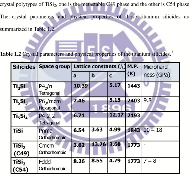
Table 1.1 Physical properties of some common used metal silicides.3
1.3 Titanium Silcide
Among the most studied silicdes, titanium silicides show higher melting points
low electrical resistivities, and lower density, which made them good candidates for
electronics technology. According to binary phase diagram of the Ti-Si system, shown
in Figure 1.1, several titanium silicides with different compositions, such as Ti3Si,
Ti5Si3, Ti5Si4, TiSi and TiSi2, could exist in the Ti-Si system.82 Besides, there are two
crystal polytypes of TiSi2, one is the metastable C49 phase and the other is C54 phase.
The crystal parameters and physical properties of those titanium silicides are
summarized in Table 1.2.3
Table 1.2 Crystal parameters and physical properties of the titanium silicides.3
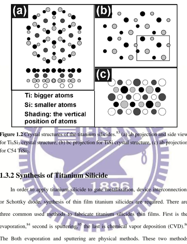
1.3.1 Structure and Properties of Titanium Silicide
The structure parameters and some physical properties of titanium silicides are
summarized in Table 1.2. The structures of Ti5Si3, TiSi and C54-TiSi2, which were
crystal structures for the titanium silicides. The bigger circles denote Ti atoms and the
smaller ones are Si atoms. The shading of the circle indicates the height above the
projection plane. From white to black represent 0, 1/4, 1/2, and 3/4 of the lattice
vector normal to the plane. Ti5Si3 possesses a hexagonal structure (Mn5Si3 type) with
space group of P63/mcm and lattice constants of a = 7.4610 Å and c = 5.1508 Å .
Figure 1.2a shows the ab projection and side view for Ti5Si3. There are two
independent crystallographic sites of Ti atoms in the Ti5Si3. These correspond to the
white and dark gray (1) and the black and light gray (2) circles. Ti1 has two Ti1 first
neighbors, six Si second neighbors, and six Ti2 third neighbors. Ti2 has two Si first
neighbors, three Si second neighbors, two Ti2 third neighbors, four Ti2 fourth
neighbors, and four Ti1 fifth neighbors. Si has two Ti2 frist neighbors, four Ti1 second
neighbors, three Ti2 third neighbors, and four Si fourth neighbors. Figure 1.2b
displays the orthorhombic TiSi structure with space group of Pnma. The lattice
constants are a = 6.54 Å , b = 3.63 Å , and c = 4.99 Å . Each Ti atom has seven Si atoms
in the range of 4.92 – 5.15 Å and six Ti atoms at 6.06 Å The Si atoms have two
nearest Si atoms and eight neighboring Ti atoms. Figure 1.2c demonstrates the ab
projection for C54 TiSi2. The structure is face-centered orthorhombic with space
group of Fddd. The lattice lattice constants are 8.26 Å , 8.55 Å , and 4.79 Å for a, b,
and c, respectively. The layer structure is an ABCD stacking of equivalent planes. Ti
has four Si first neighbors, four Si second neighbors, two Si third neighbors, and four
Ti fourth neighbors. Si has two Si first neighbors and two Ti second neighbors. Ti5Si3
has the highest melting point of 2403 K in the titanium silicides. On the other hand,
C54-TiSi2 has the lowest electrical resistance and is most used in electric device. In
the aspect of integrated circuit, TiSi2 possessed some attractive properties: (1) low
resistivity (10 – 20 mcm), (2) resist of oxidization, (3) better depression of hot electron than poly-Si made gate devices.
Figure 1.2 Crystal structures of the titanium silicides.83 (a) ab projection and side view for Ti5Si3 crystal structure, (b) bc projection for TiSi crystal structure, (c) ab projection
for C54 TiSi2.
1.3.2 Synthesis of Titanium Silicide
In order to apply titanium silicide to gate metallization, device interconnection,
or Schottky diode, synthesis of thin film titanium silicides are required. There are
three common used methods to fabricate titanium silicides thin films. First is the
evaporation,84 second is sputtering,85 the last is chemical vapor deposition (CVD).86 The Both evaporation and sputtering are physical methods. These two methods
require two experimental steps, first is deposition of Ti or codeposition of Ti and Si on
Si substrate. After that, the samples were annealed at high temperature to form
silicides. In general Ti/Si thin film system, a thin layer of amorphous TixSiy will be
formed between Ti/Si interfaces after deposition at room temperature.87 After annealing at around 673 K, the amorphous layer becomes thicker.88 At higher temperatures, Ti5Si3, Ti5Si4, TiSi and C49-TiSi2 along with amorphous TixSiy layer are
formed. When the temperature was rised to 973-1073 K, C54-TiSi2 will be the only
existing phase.87 Unfortunately, the annealing procedure usually damages the electronic devices. In the CVD method, by reaction between metal halides (TiCl4,
WF6, etc) with silane or silicon chlorides, the reaction temperature could be lower and
the annealing process is no longer necessary. Some examples of synthesis of titanium
silicide thin film are shown below;89-91
As a consequence, CVD seems to be proper method to synthesis titanium
silicides. However, the reactions required some explosive materials, such as SiH4 and
H2. A unique CVD of titanium silicides was invented by Lee in 1999.66 The reaction
pathway is proposed to the reaction between the in situ generated TiClx(x=1-3),
through reaction between TiCl4 and Ti metal, and the Si substrate. This method
provides a safe and easy way to synthesis titanium silicide.
1.4 Metal Silicide Nanowires
One-dimensional nanomaterials, such as wires, rods, belts, and tubes have
demonstrated to possess distinct properties from their bulk materials. Furthermore,
with the advancement in electronic technology, the dimensions of the electronics
devices continue to scale down. Therefore, fabrications of metal silicide
nanomaterials have turned into essential research topics. Most silicide compounds
chemical synthesis of silicide nanostructures can be quite difficult. Recently, growth
of variety of silicide nanowires has been reported. These NWs could be grouped into
two types: One is the epitaxial grown silicide NWs, which were lying on thy Si
substrates. The other is the free standing silicide NWs, which is easier to be applied
on electronic devices. The self-assembly epitaxial of rare-earth silicide NWs on Si
was first shown by Preinesberger et al.92,93 A sub-monolayer coverage of Dy on Si (001) results in the formation of nanowires under certain condition. Similar results
were then discovered for Er,94 Ho,95 Sc, and Gd96 silicides. The growth of the NWs is originated from the anisotropic lattice mismatch that is small in the long direction and
large in the short direction. Epitaxial metal silicides NWs have also been observed in
another system, such as Co/Si,97 Fe/Si,98 and Ti/Si,99 which shown the “endotaxial’ growth mechanism. The endotaxial mechanism does not require anisotropic lattice
mismatch; it allows for a variety of metal and substrates and it allows tuning of the
NW aspect ration via the growth temperature.
From the practical aspect, freestanding silicides NWs possess great potential than
the epitaxial ones. More recently, several techniques have been used to synthesize
free-standing silicide NWs, and could be classified into four groups: silicidation of Si
NWs or Metal NWs, deposition of Si source on metal films, reaction between metal
vapor sources and Si substrates, and deposition of metal and Si on the substrate
simultaneously. In addition, the application of the free-standing silicide NWs will be
1.4.1 Synthetic Methods of Metal Silicide NWs
1.4.1.1 Silicidation of Si or Metal NWs
First technique involves taking Si NWs or metal NWs as templates and then
reacting with their complementary elements, such as metal for Si NW and Si for metal
NW. Through this concept, single crystalline Pt6Si5 NWs were fabricated through
reaction between polycrystalline Pt NWs, synthesized using anodic aluminum oxide
(AAO) templates by electrochemical deposition, and SiCl4/H2. And this is the first
report of transition metal silicide NWs.62 However, the reason for the transformation of polycrystalline Pt NWs into single crystalline Pt6Si5 NWs is under investigation.
Other researches have shown fabrication of silicide NWs by evaporating metal, such
onto the Si NWs template, synthesized through typical Au nanoparticle-assist VLS
process. After annealing, metal silicide NWs were produced through solid state
reaction. NiSi NWs was first prepared and reported by Lieber et al. In addition,
epitaxial hetero junctions of NiSi/Si NWs were obtained and the NWs based
field-effect transistors were also demonstrated.44 Similar methods were applied to synthesize FeSix NWs34 and PtSi NWs.34,63 Lately, in-situ high-resolution
transmission electron microscopy (HRTEM) have exhibited powerful ability to study
the kinetics of silicidation process. Si/silicide NW heterostructures were prepared by
in situ annealing for point contact reaction between Si NWs and transition metal NWs,
Ni50 or Co,38 in an in-situ TEM. Si NWs were fabricated through Au nanocatalyst VLS method, while metal NWs were prepared via electroplating deposition Ni or Co
into AAO template. The results showed distinct diffusion behavior. Despite the low
throughput as a synthetic technique, silicidation of single Si NW is a powerful method
to study the silicidation process and may reveal the growth mechanism of other metal
1.4.1.2 Deposition of Si Sources on Metal Films
Vapor-phase synthetic routes between metal vapor phase and Si thin film or Si
vapor deposition on metal thin films and to spontaneously form various single
crystalline metal silicides NWs. These synthetic methods are simple and become
popular methods to fabricate silicide NWs. In addition, they are commonly obtained
without the presence of the catalytic metal nanoparticles on the NWs. The first
reported silicide NWs through vapor-phase reaction between Si vapor source and
metal thin film was NiSi2 NWs, which was demonstrated by Solanki et al. in 2004.43
The NiSi2 NWs was obtained by reaction between the SiH4 and the Ni thin fiim.
Several NiSix NWs with different crystal phases (NiSi2,45 NiSi,46,48,54 Ni2Si,45,54,57
Ni3Si2, 49 Ni31Si12,56 and Ni3Si55) were also reported recently. The growth mechanisms
of most of the NiSix NWs are seldom discussed. Taking Ni2Si NWs for example, SiH4
decomposes and deposits on the Ni film to grow Ni2Si nanocrystals. As the reaction
progress, elongation of the nanocrystals shrinks the sites on the surface for Ni
diffusion. After the Ni incorporation rate matches the Si deposition, Ni2Si NWs are
formed.57 On the other hand, NiOx layer, serving as a diffusion barrier for Ni, was also
regarded as an important key to the NiSix NWs growth and was reported by Jo et al.
Except NiSix NWs, Ti5Si4 nanobats were fabricated on Ti foil via a vapor and
condensation method with Si powder keeping at high temperature zone of 1373 K and
Ti foil at low temperature zone of 1173 K.21
1.4.1.3 Reaction between Metal Vapor Sources and Si Substrates
Recently, some free-standing metal silicide NWs were fabricated by reacting
pure metal vapors or anhydrous metal halides with Si substrates directly. TaSi2 NWs
were prepared through annealing samples composed with FeSi2 thin film or FeSi2
and reacted with the Si atom, segregated from the FeSix part, to form TaSi2
nanocrystals. Under proper condition, certain facets shown preferred growth and
one-dimensional nanostructure was observed. TiSi2 NWs were first synthesized by a
vapor deposition of Ti vapor onto the Si substrate in 2005.15 Anhydrous metal halides were commonly used as the transition metal sources to react with Si substrate to grow
silicide NWs. For example, FeCl3 was vaporized at about 473 K and reacted with the
Si substrate at 1373 K to form FeSi NWs.32 Through this simple concept, NWs of TiSi2,20 TiSi,22 Ti5Si3,18 CrSi2,26,29 FeSi,32 Fe5Si3,35 CoSi,37,42 Co2Si,37,42 and
Fe11-xCoxSi39 were fabricated. To date, no convincing mechanism has been porposed.
Vopor-solid (VS) mechanism is usually employied to explain the NW growth, since
the supersaturation condition of the metal halides shows great influence on the
morphology and crystal phase of the NWs.
1.4.1.4 Deposition of Metal and Si on the Substrates Simultaneously
Two techniques have been developed by transporting Si and metal sources to the
substrate simultaneously to produce silicide NWs: one is chemical vapor transport
(CVT), another is chemical vapor deposition (CVD) method. CVT method is a
conventional solid-state crystal growth technique used to grow single crystals. The
concept of CVT is exploiting the thermodynamically reversible reaction between
source materials and transport agent (usually halogens) to produce gaseous precursor
in situ. As shown in Figure 1.3a, silicide reacts with I2 at T1 to generated gaseous
product. The gaseous precursor undergoes the reverse reaction to product silicide
NWs at T2. CrSi2 NWs on Si/SiO2 substrate, with dilute Ni(NO3)2 on the surface,
were obtained using CrSi2 powder as the source material and I2 as the transport
agent.27 The Jin group has utilized the complementary chemical vapor transport (CVT) method to synthesis CrSi2 NWs. The CVT process using CrSi2 powder as the source
material and iodine as the transport reagent, which could transferred the solid CrSi2
into gaseous CrI2 and SiI4. Through CVT the reaction temperature could be lower and
the metal/silicide ration of the gaseous precousors will be similar with the desired
CrSi2 NWs, which could prevent the formation of multiple crystal phases. This CVT
method has demonstrated to be general on other silicide NWs, such as -Ni2Si52 and
-Ni3Si51 NWs were obtained using Ni2Si and TiSi2 as source materials respectively.
Figure 1.3 (a) Schematic diagram for silicide NWs synthesized by Chemical vapor
transport (CVT), (b) Synthesis of silicide NWs through single source precursor chemical vapor deposition (CVD).100
Chemical vapor deposition is commonly used to obtain transition metal silicide
thin films. Using single source precursors (SSP), consisting metal and silicon atoms,
in CVD is a simple method and allows controlling over the stoichiometry of the
oxide layer on the top, by using trans-Fe(CO)4(SiCl3)2 as precursor, which undergoes
a reductive elimination to FeSiCl2 and further decomposes into FiSi in the gas
phase.33 This technique has been extended to CoSi36 and MnSi2-x (MnSi1.8) NWs30 by
using Co(CO)4SiCl3 and Mn(CO)5SiCl3, respectively. Moreover, Mixtures of
Co(CO)4SiCl3 and trans-Fe(CO)4(SiCl3)2 can be used as precursor to obtain
Fe1-xCoxSi alloy NWs.38
CVD with Si and metal sources has been used to prepare metal silicide thin film.
Du et al. have shown the synthesis of TiSi naonpin with a particular shape on the
deposited Ti5Si3 film by CVD with TiCl4 and SiH4 as precursors.16,17 Moreover, C54
TiSi2 NWs and two-dimensional C49 TiSi2 nanonets have been obtained by using
TiCl4 and SiH4 with H2 and reported by Wang et al.19,24 The C49 TiSi2 nanonets
shows preferred growth along [100] and [001] directions and could be attributed to
the orthorhombic symmetry. Besides, single-crystalline Mn4Si7 NWs were prepared
using SiO and MnCl2 powder as the precursors.31 The SiO and MnCl2 were placed at
different temperature zones to manipulate the evaporation rate of them respectively.
The SiO and MnCl2 could react directly to form Mn4Si7. Alternatively, MnCl2 could
react with the SiCl4, gaseous byproduct of the reaction between MnCl2 and SiO, to
form Mn4Si7. Kim et al have demonstrated the synthesis of V5Si3 NWs on a V foil
substrate on Si powder. The Si and metal sources are the Si powder and VCl3,
respectively. After reaction of VCl3 and Si powder, VSi2 and gas phase SiCl4 are
formed. In situ generated SiCl4 could be served as another Si source for the growth of
V5Si3 NWs.25
1.4.2 Applications of Metal Silicide NWs
electronic devices. As the dimension of silicide was limited to nanoscale, the scale of
the devices decreases and other novel applications have been explored, such as
nanoelectronics, cathode for electron field emitter, thermoelectrics, and solar energy
conversion.
Low electrical resistivities and compatibility with silicon-base devices made
silicide NWs a promising candidate for nanoelectronic devices. Ni2Si has
demonstrated a low resistivity of 21 cm and an extremely high failure current density of 108 A/cm2.52 Electron transportation properties of other silicide NWs were also reported.36,44 Due to their low resistivity, high aspect ratio, and low work function, metal silicide NWs are promising candidates for electron field emitter. Field emission
properties of various silicide NWs have been demonstrated including TiSi2, TiSi,
Ti5Si4, Ti5Si3, CoSi,42 NiSi2,58 NiSi,48,55 Ni31Si22,56 Ni2Si,57 and TaSi2.60 The reported
turn-on fields of the NWs are in the range of 3-4 V/m. Recently, field emission properties of single NW have started to reveal the field emission mechanism in the
nanoscale.61 Metal silicides are candidates for thermoelectrics applications, which could generate electric potential through altering the temperature, and vice versa.
CrSi2 NWs has been prepared and its thermoelectric property has been studied
through a unique technique. The result indicates that the phonon-surface scattering
increased with the decreasing NW diameter at low temperature.28 Titanium silicide have shown the ability to perform solar energy assisted catalytic water splitting.101,102 TiO2/TiSi2 heterostructures, composed of C49 TiSi2 nanonets coated with a TiO2 layer,
have show a high performance in photoelectrochemical water splitting. Burgeoning
efforts have been devoted to expend the applications of silicide NWs. However,
studies of metal silicide NWs have just begun about seven years; there are still a lot of
1.5 Introduction of Electron Field Emission
Electron field emission (EFE) is a quantum tunneling phenomenon of electron
from the surface of a material subjected to a strong electric field. When a sufficiently
strong electric field was applied on a metal or semiconductor, electrons will tunnel
through the surface potential barrier of the sample surface into vacuum level. As
shown in Figure 1.4, under an applied strong electric field, the surface potential
barrier reduced and the probability for electron extracted from the surface of solid into
vacuum level increased. There is slightly difference between the field emission
theories for metal and semiconductor; we only discuss the theory for metal below.103
Figure 1.4 Energy diagram of metal-vacuum level (a) without electric field, (b) under
high electric field.
Fowler and Nordheim obtained the accurate description of field emission, based
on tunneling of electrons through the surface potential barrier, in 1928.104 Considering the emission of electrons from a object, the emission current could be defined by
multiplying the number of electrons N(W,T) and the charge on the electron D(W).
The number of emitted electrons is determined to multiply the flux of electron
overcome the potential barrier as shown below.
0 ( , ) ( ) ) , (ET e NW T DW dW J (1.4)Where E, T represent the applied electric field and the temperature, N(W,T) and D(W)
are the function of E, and T. By integrating equation (1.4), it will change into
E y v h m e T k c T k c y t h E e T E J B B 2 3 0 2 1 2 0 0 0 2 2 2 3 2 3 4 exp sin 16 ) , ( (1.5) While the time factor is
2 1 4 0 3.79 10 E y (1.6) The velocity is
y0 V (1.7)Set T approximate to zero to discuss the field emission, equation (1.5) could be shown
as F F F J 2 3 2 B exp A ) ( (1.8) while ) ( 16 A 0 2 2 3 y t e , and 2 ( ) 3 4 B 2 0 2 1 y v m e
This is known as Fowler-Nordheim equation. Under the field emission condition, y is
between 0-1, and the function of v(y) and t2(y) could be approximated to:
t2(y) = 1.1 , v(y) = 0.95- y2
By substituting the approximation above, J = I/, and F=V into equation (1.8), the expression becomes V b aV I 2exp - (1.9) where
2 1 7 2 10 44 . 1 B exp 1 . 1 A a and 2 3 B 95 . 0 b A=1.54×10⁻⁶,B=6.87×10⁷A denotes the effective emission area and is the field enhancement factor. There are three factors, , , and , in equation (1.9) could influence the magnitude of
the field emission current density. Equation (1.9) can be further expressed as ln I ln V2 a b V 1 (1.10)
As a consequence, for a field emission data, by plotting of log(I/V2) versus 1/V, a straight line with negative slope could be obtained, and was designated as F-N plot.
Through this plot, one can judge the field emission properties of a sample. When the
work function of the sample is know, the field enhancement factor could be calculated from the slope of F-N plot.
Shouldershad addressed that with a field amplification effect, which means the
electric field lines are concentrated locally around a sharp object, the required electric
field to election emission the could be lowered dramatically.105 In 1968, Spindt had demonstrated a thin film field emission device with sharp Mo emission cathode.106 As the advancement of nanotechnology, an increasing effort has been devoted to
fabricating nanomaterials for new field emitters, such as CNTs (carbon nanotubes),10 nano-diamond coated Si nanowires (NWs),11 SiC NWs and nanotubes,12,13 metal oxides14 and metal silicides. Metal silicides NWs have excellent properties such as, high aspect ration, good conductivity, high thermal stability, and compatibility with Si
1.6 Aim of This Thesis
Titanium silicides possess outstanding physical properties and are widely used in
electronic technology. The achievement in growth of metal silicide NWs represents a
significant advance for application of silicide NWs in future nanodevices. However,
free standing titanium silicides nanowires are rarely reported. This may resulted from
the lack of easy and safe way to synthesis titanium silicdes without the usage of
high-vacuum system (for PVD) or explosive materials, such as SiH4 and H2 (for
CVD). In this thesis, we provide a unique CVD method by reaction between the
TiClx(x=1-3), which is in situ generated through reaction between TiCl4 and Ti metal,
and the Si substrates to synthesis titanium silicde materials. By modifying the reaction
conditions, such as time, temperature and partial pressure of the precursor, titanium
silicide samples composed of different morphologies (nanowires, nanoplates, and thin
films) and crystal structures could be obtained. The influence of growth conditions on
the samples and the growth mechanism will be discussed in detail.
Titanium silicides have high thermal stability and low electrical resistivity. NWs
have high aspect ratio and some distinct properties. As a consequence, the obtained
titanium silicides NWs are believed to be good electric field emitters. Field emission
1.7 References
(1) Chen, L.-J. Silicide Technology for Integrated Circuits; IEE: London, 2004.
(2) Kosolapova, T. Y. Handbook of High Temperature Compounds: Properties,
Production, Applications Hemisphere Publishing Corporation: New York, 1990.
(3) Maex, K.; Rossum, M. V. Properties of Metal Silicides; IEE: London, 1995.
(4) Murarka, S. P. Silicides for VLSI Applications; Academic Press: Orlando, FL,
1983.
(5) Bucher, E.; Schultz, S.; Lux-Steiner, M. C.; Munz, P.; Gubler, U. G., F. Appl.
Phys. A 1986, 40, 71.
(6) Murarka, S. P.; Fraser, D. B. J. Appl. Phys. 1980, 51, 350.
(7) Cui, Y.; Wei, Q.; Park, H.; Lieber, C. M. Science 2003, 293, 1289.
(8) Huang, M. H.; Mao, S.; Yan, H.; Wu, Y.-Y.; Kind, H.; Weber, E.; Russo, R.; Yang,
P.-D. Science 2001, 291, 1897.
(9) Huang, Y.; Duan, X.; Wei, Q.; Lieber, C. M. Science 2001, 291, 630.
(10) Heer, W. A.; Chatelain, A.; Ugarte, D. Science 1995, 270, 1179.
(11) Tzeng, Y.-F.; Lee, Y.-C.; Lee, C.-Y.; Lin, I.-N.; H.-T., C. Appl. Phys. Lett. 2007,
91, 063117.
(12) Zhou, X.-T.; Lai, H.-L.; Peng, H.-Y.; Au, F. C.-K.; Liao, L.-S.; Wang, N.; Bello,
I.; Lee, C.-S.; Lee, S.-T. Chem. Phys. Lett. 2000, 318, 58.
(13) Wang, C.-H.; Lin, H.-K.; Ke, T.-Y.; Palathinkal, T. J.; Tai, N.-H.; Lin, I.-N.; Lee,
C.-Y.; H.-T., C. Chem. Mater. 2007, 19, 3956.
Funct. Mater. 2003, 13, 811.
(15) Xiang, B.; Wang, Q.-X.; Wang, Z.; Zhang, X.-Z.; Liu, L.-Q.; Xu, J.; Yu, D.-P.
Appl. Phys. Lett. 2005, 86, 243103.
(16) Du, J.; Du, P.-Y.; Hao, P.; Huang, Y.-F.; Ren, Z.-D.; Han, G.-R.; Weng, W.-J.;
Zhao, G.-L. J. Phys. Chem. C 2007, 111, 10814.
(17) Du, J.; Ren, Z.-D.; Tao, K.-Y.; Hu, A.-H.; Hao, P.; Huang, Y.-F.; Zhao, G.-L.;
Weng, W.-J.; Han, G.-R.; Du, P.-Y. Cryst. Growth Des. 2008, 8, 3543.
(18) Lin, H.-K.; Tzeng, Y.-F.; Wang, C.-H.; Tai, N.-H.; Lin, I.-N.; Lee, C.-Y.; Chiu,
H.-T. Chem. Mater. 2008, 20, 2429.
(19) Zhou, S.; Liu, X.-H.; Lin, Y.-J.; Wang, D.-W. Angew. Chem. Int. Ed. 2008, 47,
7681.
(20) Chang, C. M.; Chang, Y. C.; Chung, Y. A.; Lee, C. Y.; Chen, L. J. J. Phys. Chem.
C 2009, 113, 17720.
(21) Chang, C.-M.; Chang, Y.-C.; Lee, C.-Y.; Yen, P.-H.; Lee, W.-F.; Chen, L.-J. J.
Phys. Chem. C 2009, 113, 9153.
(22) Lin, H. K.; Cheng, H. A.; Lee, C. Y.; Chiu, H. T. Chem. Mater. 2009, 21, 5388.
(23) Ren, Z.; Hu, A.; Tao, K.; Du, J.; Weng, W.; Ma, N.; Du, P. Thin Solid Films 2009,
517, 5014.
(24) Zhou, S.; Liu, X.-H.; Lin, Y.-J.; Wang, D.-W. Chem. Mater. 2009, 21, 1023.
(25) In, J.; Seo, K.; Lee, S.; Yoon, H.; Park, J.; Lee, G.; Kim, B. J. Phys. Chem. C
2009, 113, 12996.
(26) Seo, K.; Varadwaj, K. S. K.; Cha, D.; In, J.; Kim, J.; Park, J.; Kim, B. J. Phys.
(27) Szczech, J. R.; Schmmitt, A. L.; Bierman, M. J.; Jin, S. Chem. Mater. 2007, 19,
3238.
(28) Zhou, F.; Szczech, J.; Pettes, M. T.; Moore, A. L.; Jin, S.; Shi, L. Nano Lett. 2007,
7, 1649.
(29) Yu, L.; Ma, Y.; Zhu, J.; Feng, H.; Wu, Q.; Lu, Y.; Lin, W.; Sang, H.; Hu, Z. J.
Phys. Chem. C 2008, 112, 5865.
(30) Higgins, J. M.; Schmitt, A. L.; Guzei, L. A.; Jin, S. J. Am. Chem. Soc. 2008, 130,
16086.
(31) Ham, M.-H.; Lee, J.-W.; Moon, K.-J.; Choi, J.-H.; Myoung, J.-M. J. Phys. Chem.
C 2009, 113, 8143.
(32) Quyang, L.; Thrall, E. S.; Deshmukh, M. M.; Park, H. Adv. Mater. 2006, 18,
1437.
(33) Schmitt, A. L.; Bierman, M. J.; Schmeisser, D.; Himpsel, F. J.; Jin, S. Nano Lett.
2006, 6, 1617.
(34) Yamamoto, K.; Kohno, H.; Takeda, S.; Ichikawa, S. Appl. Phys. Lett. 2006, 89,
083107.
(35) Varadwaj, K. S. K.; Seo, K. I., J.; Mohanty, P.; Park, J.; Kim, B. J. Am. Chem.
Soc. 2007 . 129, 8594.
(36) Schmitt, A. L.; Zhu, L.; Schmeiber, D.; Himpsel, F. J.; Jin, S. J. Phys. Chem. B
2006, 110, 18142.
(37) Seo, K.; Varadwaj, K. S. K.; Mohanty, P.; Lee, S.; Jo, Y.; Jung, M.-H.; Kim, J.;
Kim, B. Nano Lett. 2007, 7, 1240.
N. Nano Lett. 2008, 8, 2194.
(39) In, J.; Varadwaj, K. S. K.; Seo, K.; Lee, S.; Jo, Y.; Jung, M.-H.; Kim, J.; Kim, B.
J. Phys. Chem. C 2008, 112, 4748.
(40) Schmitt, A. L.; Higgins, J. M.; Jin, S. Nano Lett. 2008, 8, 810.
(41) Seo, K.; Lee, S.; Yoon, H.; In, J.; Varadwaj, K. S. K.; Jo, Y.; Jung, M. H.; Kim, J.;
Kim, B. ACS Nano 2009, 3, 1145.
(42) Tsai, C. I.; Yeh, P. H.; Wang, C. Y.; Wu, H. W.; Chen, U. S.; Lu, M. Y.; Wu, W.
W.; Chen, L. J.; Wang, Z. L. Cryst. Growth Des. 2009, 9, 4514.
(43) Decker, C. A.; Solanki, R.; Freeouf, J. L.; Carruthers, J. R.; Evans, D. R. Appl.
Phys. Lett. 2004, 84, 1389.
(44) Wu, Y.; Xiang, J.; Yang, C.; Lu, W.; Lieber, C. M. Nature 2004, 430, 61.
(45) Yan, X. Q.; Yuan, H. J.; Wang, J. X.; Liu, D. F.; Zhou, Z. P.; Gao, Y.; Song, L.;
Liu, L. F.; Zhou, W. Y.; Wang, G.; Xie, S. S. Appl. Phys. A 2004, 79, 1853.
(46) Kim, J.; Anderson, W. A. Thin Solid Films 2005, 483, 60.
(47) Weber, W. M.; Geelhaar, L.; Graham, A. P.; Unger, E.; Duesberg, G. S.; Liebau,
M.; Pamler, W.; Cheze, C.; Riechert, H.; Lugli, P.; Kreupl, F. Nano Lett. 2006, 6,
2660.
(48) Kim, C.-J.; Kang, K.; Woo, Y. S.; Ryu, K.-G.; Moon, H.; Kim, J.-M.; Zang, D.-S.;
Jo, M.-H. Adv. Mater. 2007, 19, 3637.
(49) Kim, J.; Shin, D. H.; Lee, E.-S.; Han, C.-S.; Park, Y. C. Appl. Phys. Lett. 2007,
90, 253103.
(50) Lu, K.-C.; Wu, W.-W.; Wu, H.-W.; Tanner, C. M.; Chang, J. P.; Chen, L. J.; Tu, K.
(51) Song, Y.; Jin, S. Appl. Phys. Lett. 2007, 90, 173122.
(52) Song, Y.; Schmitt, A. L.; Jin, S. Nano Lett. 2007, 7, 965.
(53) Geng, Z. R.; Lu, Q. H.; Yan, P. X.; Yan, D.; Yue, G. H. Phys. E 2008, 41, 185.
(54) Kang, K.; Kim, S.-K.; Kim, C.-J.; Jo, M.-H. Nano Lett. 2008, 8, 431.
(55) Kim, J.; Lee, E.-S.; Han, C.-S.; Kang, Y.; Kim, D.; Anderson, W. A.
Microelectron. Eng. 2008, 85, 1709.
(56) Lee, C.-Y.; Lu, M.-P.; Liao, K.-F.; Wu, W.-W.; Chen, L.-J. Appl. Phys. Lett. 2008,
93, 113109.
(57) Liu, Z. H.; Zhang, H.; Wang, L.; Yang, D. R. Nanotechnology 2008, 19, 375602.
(58) Lee, C. Y.; Lu, M. P.; Liao, K. F.; Lee, W. F.; Huang, C. T.; Chen, S. Y.; Chen, L.
J. J. Phys. Chem. C 2009, 113, 2286.
(59) Chueh, Y. L.; Chou, L. J.; Cheng, S. L.; Chen, L. J.; Tsai, C. J.; Hsu, C. M.; Kung,
S. C. Appl. Phys. Lett. 2005, 87, 223113.
(60) Chueh, Y.-L.; Ko, M.-T.; Chou, L.-J.; Chen, L.-J.; Wu, C.-S.; Chen, C.-D. Nano
Lett. 2006, 6, 1637.
(61) Kim, J. J.; Shindo, D.; Murakami, Y.; Xia, W.; Chou, L.-J.; Chueh, Y.-L. Nano
Lett. 2007, 7, 2243.
(62) Lu, J.-L.; Zhu, J. Adv. Mater. 2003, 15, 579.
(63) Liu, B.-Z.; Wang, Y.-F.; Dilts, S.; Mayer, T. S.; Mohney, S. E. Nano Lett. 2007, 7,
818.
(64) Lu, K.-C.; Tu, K.-N.; Wu, W.-W.; Chen, L.-J.; Yoo, B.-Y.; Myung, N. V. Appl.
(65) Lin, Y.-C.; Lu, K.-C.; Wu, W.-W.; Bai, J.-W.; Chen, L.-J.; Tu, K.-N.; Huang, Y.
Nano Lett. 2008, 8, 913.
(66) Lee, C.-Y. Chem. Vap. Deposition 1999, 5, 69.
(67) Nicolet, M. A. Thin Solid Films 1978, 52, 415.
(68) Ho, P. S. Thin Solid Films 1982, 96, 301.
(69) Tu, K. N. J. Vac. Sci. Technol. 1981, 19, 766.
(70) Yu, A. Y. C. Solid State Electron 1970, 13, 239.
(71) Murarka, S. P. J. Vac. Sci. Technol. 1980, 17, 775.
(72) Geipel, H. J.; Hsieh, J. N.; Ishaq, M. H.; Koburger, C. W.; White, F. R. IEEE
Trans. Electron Devices 1980, ED-27, 1417.
(73) Murarka, S. P.; Fraser, D. B. J. Appl. Phys. 1980, 51, 342.
(74) Saxena, A. N.; Pramanik, D. Solid State Electron 1984, 27, 1984.
(75) Sinha, A. K. J. Vac. Sci. Technol. 1981, 19, 778.
(76) Kawamura, T.; Shinoda, D.; Muta, H. Appl. Phys. Lett. 1967, 11, 1967.
(77) Buckley, W. D.; Moss, S. C. Solid State Electron 1972, 15, 1331.
(78) Gurp, G. J.; Langereis, C. J. Appl. Phys. 1975, 46, 431.
(79) Borisenko, V. E. Semiconduction Silicides; Springer: Berlin, 2000; Vol. 39.
(80) Rowe, D. M. CRC Handbook of Thermoelectrics; CRC Press: Boca Raton, 1994.
(81) Senthilarasu, S.; Sathyamoorthy, R.; Lalitha, S. Sol. Energy Mater. Sol. Cells
2004, 82, 299.
(82) Massalski, T. B.; Okamoto, H.; Subramanian, P. R.; Kacprzak, L. Binary Alloy
(83) Ekman, M.; Ozolins, V. Physical Review B 1998, 57, 4419.
(84) Chopra, K. L. Thin Film Phenomena; McGraw-Hill: New York, 1969.
(85) Hoffman, D. W.; Thronton, J. A. Thin Solid Films 1977, 40, 355.
(86) Ilderem, V.; Reif, R. J. Electronchem. Soc. 1988, 135, 2590.
(87) Wang, M. H.; Chen, L. J. J. Appl. Phys. 1992, 71, 5918.
(88) Lur, W.; Chen, L. J. Appl. Phys. Lett. 1989, 54, 1217.
(89) Yim, W. M.; Stotko, E. J. J. Electrochem. Soc. 1974, 121, 965.
(90) Lacombe, J.; Duchemin, J. P.; Bonnet, M.; Huyghe, D. Eectron. Lett. 1977, 13,
472.
(91) Hallais, J. P.; Boccon-Gibod, D.; Chane, J. P.; Durand. J. Electrochem. Soc. 1977,
124, 1290.
(92) Preinesberger, C.; Vandre, S.; Kalka, T.; Dahne, M. J. Phys. D 1998, 31, L43.
(93) Preinesberger, C.; Becker, S. K.; Vandre, S.; Kalka, T.; Dahne, M. J. Appl. Phys.
2002, 91, 1695.
(94) Chen, Y.; Ohlberg, D. A. A.; Medeiros, R. G.; Chang, Y.-A.; Williams, R. S. Appl.
Phys. Lett. 2000, 76, 4004.
(95) Nogami, J.; Liu, B. Z.; Katkov, M. V.; Ohbuchi, C.; Birge, N. O. Physical Review
B 2001, 63, 233305.
(96) Chen, Y.; Ohlberg, D. A. A.; Williams, R. S. J. Appl. Phys. 2002, 91, 3213.
(97) He, Z.; Smith, D. J.; Bennett, P. A. Phys. Rev. Lett. 2004, 93, 256102.
(98) Liang, S.; Islam, R.; Smith, D. J.; Bennett, P. A. J. Cryst. Growth 2006, 295, 166.
(100) Schmitt, A. L.; Higgins, J. M.; Szczech, J. R.; Jin, S. J. Mater. Chem. 2010, 20,
223.
(101) Li, Q.; Lu, G. Catal. Lett. 2008, 125, 376.
(102) Peter, R.; Andriy, K.; Marc, A. W. t.; Klaus, K.; Claudia, W.; Martin, D. Angew.
Chem., Int. Ed. 2007, 46, 7770.
(103) Zhu, W. Vacuum Microelectronics; John Wiley, 2001.
(104) Fowler, R. H.; Nordheim, L. W. Proc. R. Soc. London, Ser. A 1928, 119, 173.
(105) Buck, D. A.; Shoulders, K. R. “An Approach to Microminiature Systems”;
Procedure Eastern Joint Computer Conference, 1958.
(106) Spindt, C. A.; Brodie, I.; Humphrey, L.; Westerberg, E. R. J. Appl. Phys. 1976,
Chapter 2
Ti
5Si
3Nanowire and Its Field Emission Property
2.1 Introduction
Because of their distinct properties, 1D nanostrutures have attracted tremendous
amounts of attention for technological applications, such as sensors,1 laser devices,2 and electrical systems.3 An increasing effort has been devoted to fabricating nanomaterials for new field emitters, such as CNTs (carbon nanotubes),4 nano-diamond coated Si nanowires (NWs),5 SiC NWs and nanotubes,6 metal oxides7 and metal silicides.8 Many studies about the fabrication of free standing silicide nanowires of Ti, Cr, Fe, Co, Ni and Ta have been reported because of their superior
properties and compatibility with Si based integrated circuit devices.8-14Among them, titanium silicides are potential candidates for field emission devices due to their
relative low resistivity (10 – 28 Ω cm), high thermal stability, and low work function.15-17 Research on the fabrication of TiSi and TiSi2 NWs and arrays through
various processing techniques, including chemical vapor deposition (CVD) and
physical vapor deposition (PVD), have been demonstrated recently.9,18-20 On the other hand, fabrication of nanostructures of metal-rich titanium silicide Ti5Si3, which is a
suitable refractory material with a melting point 2403 K, has not been reported. In this
work, we report the first growth of Ti5Si3 NWs via a unique CVD process.21
2.2 Experimental Section
2.2.1 Materials
Reagent
Chemical
Formula
Purity Vendor
Titanium (IV) chloride
TiCl
499 %
Fluka
Titanium powder(~320 mesh)
Ti
99.7 %
Aldrich
Si wafer (n-type)
orientation (100)
Si
-
Semiconductor
Wafer
Ammonium hydroxide
NH
4OH
25 %
Fluka
Hydrochloric acid
HCl
37 %
Aldrich
Hydrofluoric acid
HF
48 %
Aldrich
Hydrogen peroxide
H
2O
230 %
Aldrich
Nitric acid
HNO
370 %
Showa
Sulfuric acid
H
2SO
495 %
Fluka
Argon
Ar
99 %
Chiah Lung
2.2.2 Synthesis Procedure
All reactions were performed in a low-pressure horizontal hot-wall quartz tube
reactor comprised of a pumping system, a reaction chamber heated by a three-zone
tube furnace, and a precursor inlet control system. Ti powders (0.3 g) were placed at
the highest temperature zone at 1173 K, which is the most upstream among the
heating zones. Si (100) wafers, cleaned by RCA process and then immersed in a 48%
HF/DI water (1/100 v/v) solution until the surface became hydrophobic right before
the chamber was evacuated to 0.4 Pa, TiCl4 was vaporized into the reaction chamber
at a pressure of 2.67 Pa. After 1 - 6 h, the supply of TiCl4 was stopped and the reaction
system was cooled to room temperature. Samples of gray thin films deposited on Si
substrates were collected for analysis. A summary of the representative samples
prepared in this study is listed in Table 2.1.
Figure 2.1 Experimental setup of the CVD system.
2.2.3 Characterization Instruments
The SEM and EDX data were collected using JEOL JSM-6330F and Hitachi
S-4700I at 15 kV. The TEM and SAED images were obtained on a JEOL JEM-2010
at 200 kV. The HRTEM images were acquired on a JEOL JEM-400EX at 400 kV. The
Auger depth profile was obtained on a Physical Electronics Auger 670 PHI Xi. The
XRD studies were carried out using a MAC MXP-18 and a BRUKER AXS D8
ADVANCE with Cu K1 radiation. The EFE properties of the samples were measured in a vacuum chamber at a pressure of 1.05 10-3 Pa at room temperature with a spherical-shaped stainless-steel probe of 1 mm in diameter as the anode. The
m, 135 m, and 100 m for samples I, II, and III respectively. The current-voltage (I-V) characteristics were measured using a Keithley 237. The maximum available
voltage of the set-up is 1100 V, and the current was restricted to 10 mA.
Figure 2.2 Setup of the home-built electron field emission (EFE) system.
2.3 Results and Discussion
All reactions were performed in a low pressure horizontal hot-wall quartz tube
reactor heated by a three-zone tube furnace. TiCl4, the precursor, was vaporized into
the reaction chamber at a controlled partial pressure. Close to the precursor inlet, Ti
powders were placed at the heating zone at 1173 K. Si (100) wafers were placed at the
center heating zone at 773 - 973 K. After 1 - 6 h, deposition of a gray layer on the
substrates was observed. A summary of the representative samples prepared in this

![Figure 2.6 TEM studies of a NW isolated from I. (a) Low magnification image, (b) SAED pattern of the sample in (a) showing a [1 1 0] zone axis, (c) high-resolution image from the selected section in (a)](https://thumb-ap.123doks.com/thumbv2/9libinfo/8621970.191604/51.892.134.760.363.860/figure-isolated-magnification-pattern-showing-resolution-selected-section.webp)
