行政院國家科學委員會專題研究計畫 成果報告
極紫外光(EUV)微影技術從光源建造、光罩、材料、製程到
奈米元件可靠度研究(3/3)
研究成果報告(完整版)
計 畫 類 別 : 整合型 計 畫 編 號 : NSC 99-2120-M-009-004- 執 行 期 間 : 99 年 08 月 01 日至 100 年 07 月 31 日 執 行 單 位 : 國立交通大學電子工程學系及電子研究所 計 畫 主 持 人 : 黃遠東 共 同 主 持 人 : 許博淵、鄭秀英、馮學深、劉致為、蔡坤諭 李佳翰、林俊宏、崔秉鉞、謝健 計畫參與人員: 碩士級-專任助理人員:王孟坤 碩士班研究生-兼任助理人員:林奕名 碩士班研究生-兼任助理人員:林玉珠 碩士班研究生-兼任助理人員:梁家慶 碩士班研究生-兼任助理人員:林茜荷 碩士班研究生-兼任助理人員:曾宇鋕 碩士班研究生-兼任助理人員:張柏森 碩士班研究生-兼任助理人員:錢盛偉 碩士班研究生-兼任助理人員:張克勤 碩士班研究生-兼任助理人員:孫銘鴻 碩士班研究生-兼任助理人員:劉芳宜 碩士班研究生-兼任助理人員:蘇婷婷 碩士班研究生-兼任助理人員:宋佳展 碩士班研究生-兼任助理人員:黃彥翔 碩士班研究生-兼任助理人員:陳威霖 碩士班研究生-兼任助理人員:何叔憶 碩士班研究生-兼任助理人員:朱冠宇 碩士班研究生-兼任助理人員:張櫻諭 博士班研究生-兼任助理人員:陳建華 博士班研究生-兼任助理人員:張環麟 博士班研究生-兼任助理人員:鄭信鴻報 告 附 件 : 出席國際會議研究心得報告及發表論文
公 開 資 訊 : 本計畫可公開查詢
中 文 摘 要 : 半導體相關工業是台灣的兆元產業,但是因應次世代微影技 術發展,之前並無極紫外光微影技術相關的大型研究計畫。 本計畫嘗試整合國家實驗室(國家同步輻射中心、國家奈米元 件實驗室)與大學(交通大學、台灣大學、成功大學與高雄大 學)之儀器與人力資源以啟動台灣極紫外光微影技術之相關技 術研究。此計畫主要是建立在極紫外光微影技術中最必要的 技術--分析和檢測技術。 本計畫根據工作屬性區分為(I)基礎研發、(II)光學與檢測技 術、以及(III)極紫外光微影技術之相關應用研究等三組。其 中(I)基礎研發的主要目的是建立基礎的儀器設備(極紫外光 微影技術之光束線、反射儀和光化學檢測平台)以量測分析基 本的材料性質與行為;(II)光學與檢測技術的主要目的是研 發創新的檢測設備(高效率光罩檢測與極紫外光微影技術之干 涉微影設備)以進一步提升極紫外光微影技術之檢測應用;極 (III)紫外光微影技術之相關應用研究的主要目的則是研究探 討極紫外光微影技術應用於元件製造時可能發生的關鍵問題 (輻射損傷、抗反射層、混合微影製程和奈米元件圖形化製程 之研究),以提供可行的解決方案。 中文關鍵詞: 次世代微影技術,極紫外光微影技術(EUVL),半導體製程, 同步輻射光源,EUVL 檢測技術
英 文 摘 要 : The semiconductor industry is the major business in Taiwan. However, almost no effort has been done on EUVL for the NGL technology before. In this project, we attempt integrating the resources from the
National Labs (NSRRC, NDL) and universities (NCTU, NTU, NCKU, NKU) to initiate the EUVL research program in Taiwan. In this project, we focus on developing EUV analytical and metrology technologies because they will be the most-required technologies if EUVL is on.
All the works in this project are divided into three groups of (I) Fundamentals, (II) Optics and
Metrology, and (III) EUVL Applications. The object of group I (Fundamentals) is to establish the
infrastructures (EUVL beamline, reflectometer and resist evaluation platform) to measure and analyze the basic material properties and behaviors in the EUV range. The object of group II (Optics and Metrology) is to develop novel instruments
(High-throughput mask inspection system, EUV
interferometer) for EUVL metrology applications. The object of group III (EUVL Applications) is to explore the critical issues in device fabrication (radiation damage, anti-reflection coating, mix/match processes, and nano-device paterning) with EUV lithography.
英文關鍵詞: Next generation lithography (NGL), Extreme UV lithography (EUVL), Semiconductor, Synchrotron radiation, EUV metrology technology
奈米國家型科技計畫研究重要成果
1. 計畫背景:
計畫主持人及共同主持人(PI and Co-PIs):
PI (計畫主持人): 1 黃遠東(Yang-Tung Huang) Co-PIs (共同主持人): 2 許博淵(Bor-Yuan Shew),3 鄭秀英(Grace H. Ho),2 馮學深(Hok-Sum Fung),4 劉 致為(Chee-Wee Liu),4 蔡坤諭(Kuen-Yu Tsai),5 李佳翰(Jia-Han Li),6 林俊宏
(Chun-Hung Lin),1崔秉鉞(Bing-Yue Tsui),7
謝健(Jiann Shieh)
研究題目(Project Title):
極紫外光微影技術從光源建造、光罩、材料、製程到奈米元件可靠度研究 3/3 (Investigations on extreme ultraviolet lithography from beamline construction, masks, materials, processes, to reliability of nano devices 3/3)
主持人執行機構(Organization):
1
國立交通大學電子工程學系
(Dept. of Electronics Eng., National Chiao Tung University) 2
國家同步輻射研究中心實驗設施組
(National Synchrotron Radiation Research Center) 3
國立高雄大學應用化學系
(Dept. of Applied Chemistry, National University of Kaohsiung) 4
國立臺灣大學電機工程學系
(Dept. of Electrical Eng., National Taiwan University) 5
國立臺灣大學工程科學及海洋工程學系
(Dept. of Eng. Science and Ocean Eng., National Taiwan University) 6
國立成功大學光電科學與工程研究所
(Institute of Electro-Optical Science and Eng., National Cheng-Kung University) 7
國家奈米元件實驗室
(National Nano Device Laboratory)
全程計畫執行期限(Project period):
自民國九十七年八月一日至民國一百年七月三十一日 From 2008/08/01 to 2011/07/31.
分年經費(Budget per year):
第一年:680 萬元,第二年:680 萬元,第三年:480 萬元 1st year: 6,800k, 2nd year: 6,800k, 3rd year: 4,800k (TWD)
2. 計畫目標:
半導體相關工業是台灣的兆元產業,但是因應次世代微影技術發展,之前並無 極紫外光微影技術相關的大型研究計畫。本計畫嘗試整合國家實驗室(國家同步輻射 中心、國家奈米元件實驗室)與大學(交通大學、台灣大學、成功大學與高雄大學)之 儀器與人力資源以啟動台灣極紫外光微影技術之相關技術研究。此計畫主要是建立 在極紫外光微影技術中最必要的技術--分析和檢測技術。 關鍵辭: 次世代微影技術,極紫外光微影技術(EUVL),半導體製程,同步輻射光源, EUVL 檢測技術 本計畫根據工作屬性區分為(I)基礎研發、(II)光學與檢測技術、以及(III)極紫外 光微影技術之相關應用研究等三組。其中(I)基礎研發的主要目的是建立基礎的儀器 設備(極紫外光微影技術之光束線、反射儀和光化學檢測平台)以量測分析基本的材料 性質與行為;(II)光學與檢測技術的主要目的是研發創新的檢測設備(高效率光罩檢測 與極紫外光微影技術之干涉微影設備)以進一步提升極紫外光微影技術之檢測應 用;極(III)紫外光微影技術之相關應用研究的主要目的則是研究探討極紫外光微影技 術應用於元件製造時可能發生的關鍵問題(輻射損傷、抗反射層、混合微影製程和奈 米元件圖形化製程之研究),以提供可行的解決方案。Keywords: Next generation lithography (NGL), Extreme UV lithography (EUVL), Semiconductor, Synchrotron radiation, EUV
metrology technology
The semiconductor industry is the major business in Taiwan. However, almost no effort has been done on EUVL for the NGL technology before. In this project, we attempt integrating the resources from the National Labs (NSRRC, NDL) and universities (NCTU, NTU, NCKU, NKU) to initiate the EUVL research program in Taiwan. In this project, we focus on developing EUV analytical and metrology technologies because they will be the most-required technologies if EUVL is on.
All the works in this project are divided into three groups of (I) Fundamentals, (II) Optics and Metrology, and (III) EUVL Applications. The object of group I (Fundamentals) is to establish the infrastructures (EUVL beamline, reflectometer and resist evaluation platform) to measure and analyze the basic material properties and behaviors in the EUV range. The object of group II (Optics and Metrology) is to develop novel instruments (High-throughput mask inspection system, EUV interferometer) for EUVL metrology applications. The object of group III (EUVL Applications) is to explore the critical issues in device fabrication (radiation damage, anti-reflection coating, mix/match processes, and nano-device paterning) with EUV lithography.
3. 參與計畫單位及人數:
1國立交通大學電子工程學系 (Dept. Electronics Eng.,NCTU)
1 Research Assistant; 3 Phd students; 2 Master student; 1 college student) 2國家同步輻射研究中心 (National Synchrotron Radiation Research Center) 一位副研究員,一位助理研究員(2 Associate Scientist, 1 Assistant Scientist) 3國立高雄大學應用化學系 (Dept. Applied Chemistry, NUK)
一位副教授;二位碩士生 (1 Associate Professor; 2 Master students) 4國立臺灣大學電機工程學系(Dept. Electrical Eng., NTU)
一位教授,一位助理教授,三位博士生,二位碩士生 (1 Professor; 1 Assistant Professor; 3 Phd student, 2 Master students)
5國立臺灣大學工程科學及海洋工程學系(Dept. Eng. Sci.& Ocean Eng., NTU) 一位助理教授;一位博士生;二位碩士生 (1 Assistant Professor; 1 Phd student;
2 Master students)
6國立成功大學光電科學與工程研究所 (Institute of Electro-Optical Sci.& Eng.,
NCKU)
一位助理教授;二位碩士生;一位大學生 (1 Assistant professor; 2 Master students; 1 college student)
7
國家奈米元件實驗室(National Nano Device Laboratory)
一位副研究員;一位博士生 (1 Associate Researcher; 1 Phd student)
4. 每半年列出最具代表性之論文或專利
6 篇
:
2008.07~2008.11
[1] G. H. Ho, C.-J. Liu, C.-H. Yen, M.-H. Ho and S.-Y. Wu, “ Ionic outgassing from photoacid generators upon irradiation at 13.5 nm”, Microelectron. Eng., 85 (11), pp. 2213 – 2219, 2008
[2] B.-Y. Tsui, C.-P. Lu, and H.-H. Liu, “Method for Extracting Gate Voltage Dependent Source Injection Resistance of Modified Schottky Barrier (MSB) MOSFETs,” IEEE Electron Device Lett., vol.29, No.9, pp.1053-1055, 2008.
[3] J. Li and K. J. Webb, “Influence of granularity on the optical properties of a negative-refractive-index lens,” Physical Review A, vol. 78, 015803, Jul. 2008,. [4] H. L. Chen, K. C. Hsieh, C. H. Lin, and S. H. Chen, “Using direct nanoimprinting
of ferroelectric films to prepare devices exhibiting bi-directionally tunable surface plasmon resonances,” Nanotechnology 19, 435304 (2008).
[5] C. H. Lin, J. Shieh, W.H. Chang and B.T. Dai, “Influence of mask magnification effects on the diffracted light and lithographic imaging for EUV phase shifting mask,” 34th International Conference on Micro & Nano Engineering (MNE), OL-P10, Athens/Greece, 15-18 Sep. 2008.
EUVL Symposium, Lake Tahoe, California, October 1, 2008.
2008.12~2009.05
[1] W. S. Ho, C.-H. Lin, T.-H. Cheng, W. W. Hsu, Y. -Y. Chen, P. -S. Kuo, and C. W. Liu, “Narrow-Band Metal-Oxide-Semiconductor Photodetectors,” Appl. Phys. Lett., Vol. 94, 061114, 2009.
[2] P.-S. Kuo, C.-Y. Peng, C.-H. Lee, Y.-Y. Shen, H.-C. Chang, and C. W. Liu,
“Si/Si0.2Ge0.8/Si quantum well Schottky barrier diodes,” Appl. Phys. Lett., Vol. 94, 103512, 2009.
[3] C.-Y. Peng, Y.-C. Fu, C.-F. Huang, Y.-J. Yang, M.H. Liao, S.-T. Chang, and C.W. Liu, “Strain-Induced Flat-band Voltage Shift of Metal-Oxide-Silicon Capacitors,” accepted by IEEE Trans. on Electron Devices., 2009.
[4] G. H. Ho, F.-H. Kang, Y.-H. Shih, H.-S. Fung, H.-W. Fu, R. Sakamoto, T. Endo, B.-C. Ho, Y.-T. Huang, and B.-Y. Shew, “EUV Reflectometry for Determining the Optical Properties of Photoresists and Underlayer Materials upon Irradiation at 13.5 nm”, 2009 Internatioanl workshop on EUV lithography, July 13-17, 2009, Honolulu, Hawaii.
[5] G. H. Ho, Y.-H. Shih, and F.-H. Kang, “Absolute Total Ion Yield and the Relative Extent of Ionic Outgassing of Photoresists and Underlayer Materials upon Irradiation at 13.5 nm”, 2009 Internatioanl workshop on EUV lithography, July 13-17, 2009, Honolulu, Hawaii.
[6] H.-W. Fu, G. H. Ho, L.-J. Huang, C.-F. Chang,1 S.-W. Lin, S.-W. Luo, F.-H. Kang, Y.-H. Shih, H.-S. Fung, and B.-Y. Shew, “A Compact and Ultrahigh-vacuum Reflectometer for EUV Applications “, 2009 Internatioanl workshop on EUV
lithography, July 13-17, 2009, Honolulu, Hawaii.
2009.06~2009.11
[1] W. S. Ho, C.-H. Lin, T.-H. Cheng, W. W. Hsu, Y. -Y. Chen, P. -S. Kuo, and C. W. Liu, “Narrow-Band Metal-Oxide-Semiconductor Photodetectors,” Appl. Phys. Lett., Vol. 94, 061114, 2009.
[2] Y.-L. Yang, S.-H. Hsu, M.-F. Lu, and Y.-T. Huang, “Photonic Crystal Slab Waveguides Based on Antiresonant Reflecting Optical Waveguide Structures,”
IEEE Journal of Lightwave Technology, Vol. 27, No. 14, pp. 2642-2648, July
2009.
[3] Jia-Han Li, Yi-Wei Cheng, Yu-Cheng Chue, Chih-Hung Lin, and Tony Wenn-Hann Sheu, , “The Influence of Propagating and Evanescent Waves on
18462-18468, Oct. 2009..
[4] Jiann Shieh, Fu Ju Hou, Yan Chen Chen, Hung Min Chen, Shun Po Yang, Chao Chia Cheng, Hsuen Li Chen, “Robust airlike superhydrophobic surfaces” Advanced Materials, Published Online, Nov. 2, 2009.
[5] Ting-Hang Pei, Kuen-Yu Tsai, and Jia-Han Li, “Effects of Fresnel Zone Plate Fabrication Errors on Focusing Performance,” The 22nd International
Microprocesses and Nanotechnology Conference (MNC 2009).
[6] G. H. Ho, Y.-H. Shih, F.-H. Kang, H.-W. Fu, H.-S. Fung, W.-P. Ku, Y.-H. Cheng, and P.-J. Wu, “Absorption and outgassing of photoresists and underlayer materials upon irradiation at 13.5 nm”, SPIE proceedings on Advanced Lithography, 21-25 February 2010, San Jose, United States.
2009.12~2010.05
[1] Chi-Pei Lu, Cheng-Kei Luo, Bing-Yue Tsui, Cha-Hsin Lin, Pei-Jer Tzeng,
Ching-Chiun Wang, and Ming–Jinn Tsai, “Tri-gate TiN Nanocrystal Memory with Higk-k Blocking Dielectric Layer and High Work Function Gate Electrode,”
Electrochem. and Solid-State Lett., vol. 12, no. 3, pp. H70-H72, 2009.
[2] Chi-Pei Lu, Cheng-Kei Luo, Bing-Yue Tsui, Cha-Hsin Lin, Pei-Jer Tzeng, Ching-Chiun Wang, and Ming–Jinn Tsai, “Nanoscale Multigate TiN Metal
Nanocrystal Memory Using High-k Blocking Dielectric and High-Work-Function Gate Electrode Integrated on Silcon-on-Insulator Substrate,” Jap. Journal of
Applied Physics, vol. 48, 04C059, 2009.
[3] Jiann Shieh, Fu Ju Hou, Yan Chen Chen, Hung Min Chen, Shun Po Yang, Chao Chia Cheng, Hsuen Li Chen, “Robust airlike superhydrophobic surfaces”
Advanced Materials, vol. 22, pp. 597-601, 2010.
[4] M.-F. Lu, S.-M. Liao, and Y.-T. Huang, “Ultra Compact Photonic Crystal
Polarization Beam Splitter Based On Multimode Interference,” Applied Optics, Vol. 49, No. 4, pp. 724-731, Feb. 2010.
[5] Grace H. Ho, Yu-H. Shih, Fu-H. Kang, Jia-C. Hung, Chih-H. Shao, Yu-H. Lai, “Photochemistry of photoresists and underlayer materials upon irradiation at 13.5nm”, J. Photochem. Photobiol. A: Chem, vol. 211, pp. 78-87, 2010.
[6] Kuen-Yu Tsai, Sheng-Yung Chen, Ting-Han Pei, and Jia-Han Li, “Fresnel Zone Plate Manufacturability Analysis for Direct-Write Lithography by Simulating Focusing and Patterning Performance versus Fabrication Errors,” Jpn. J. Appl.
Phys., vol. 49, no. 6, pp. 06GD08-06GD08-6, 2010..
2010.06~2010.11
[1] Grace H. Ho, Fu-H. Kang, Chih-H. Shao, Wei-L. Hung, Chih-B Kao, and Yu-L. Chou, “Outgassing and extreme-ultraviolet photochemistry of photoresist and underlayer materials,” 2010 International Workshop on EUV lithography, Hawaii, Maui, USA, June 22-25, 2010. (oral presentation)
“Flexible Ge-on-Polyimide detectors,” Appl. Phys. Lett., Vol. 94, 261107, 2009. [3] Bing-Yue Tsui, Chih-ChanYen, Po-Hsueh Li, Chih-Pei Lu, Jui-Yao Lai, “Extreme
Ultra-Violate Exposure Induced Damages on Non-Volatile Memories,” 2010 IEEE
Silicon Nanoelectronics Workshop, 2010.
[4] Sheng-Yung Chen, Shin-Chuan Chen, Hsing-Hong Chen, Kuen-Yu Tsai, and Hsin-Hung Pan, “Manufacturability analysis of a MEMS-based electron-optical system design for direct-write lithography,” Japanese Journal of Applied Physics, vol. 49, p 06GE05, Jun. 2010.
[5] Ting-Hang Pei, Kuen-Yu Tsai, and Jia-Han Li, “Stochastic simulation of photon propagation in Si for extreme-ultraviolet mask-defect inspection,” Applied Physics
Letters, vol. 97, no. 6, p 061108, Aug. 2010.
[6] Yen-Min Lee, Jia-Han Li, Philip C. W. Ng , Ting-Han Pei, Fu-Min Wang, Kuen-Yu Tsai, and Alek C. Chen, “Efficient scattering simulations for equivalent extreme ultraviolet mask multilayer structures by modified transmission line theory and finite-difference time-domain method,” Journal of
Micro/Nanolithography, MEMS, and MOEMS (JM3), vol. 9, no. 4, pp.043003-1 to
043003-15, Oct.-Dec. 2010. 2010.12~2011.07
[1] T.-H. Pei and Y.-T. Huang, “The High-Transmission Photonic Crystal Heterostructure Y-branch Waveguide Operating at Photonic Band Region,”
Journal of Applied Physics, Vol. 109, 034504, Feb. 2011.
[2] Philip C. W. Ng, Kuen-Yu Tsai, Yen-Min Lee, Fu-Min Wang, Jia-Han Li, and Alek C. Chen, “Fully model-based methodology for simultaneous correction of
extreme ultraviolet mask shadowing and proximity effects,”Journal of
Micro/Nanolithography, MEMS, and MOEMS (JM3), vol. 10, No. 1, pp.
013004-1-013004-13, Jan.-Mar. 2011
[3] C.H. Lin, C.H. Fong, Y.M. Lin, Y.Y. Lee, H.S. Fung, B.Y. Shew, and J. Shieh, “EUV interferometric lithography and structural characterization of an EUV diffraction grating with nondestructive spectroscopic ellipsometry,”
Microelectron. Eng. (published online, http://dx.doi.org/10.1016/j.mee.2011.02.002).
[4] Y. M. Chang, J. Shieh, and J. Y. Juang, “Sub-Wavelength Antireflective Si Nanostructures Fabricated by Using the Self-Assembled Silver
Metal-Nanomask”J. of Physical Chemistry C 115, 8983-8987, 2011. ( SCI/2009: 4.224)
[5] Jiann Shieh, Srikanth Ravipati, Fu Hsiang Ko, Kostya (Ken) Ostrikov, “Plasma-made silicon nanograss and related nanostructures” J. Phys. D: Applied Physics 44, 174010 , 2011. (invited) (SCI/2009: 2.083)
Ko, 2010/12“Fabrication and Enhanced Field Emission Properties of Novel Silicon Nanostructures”Microelectronics Reliability 50, 1973-1976, 2010. (SCI/2009: 1.152)
1. 計畫已獲得之主要成就與成果:
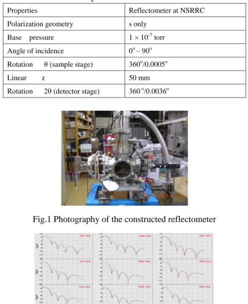
2008.08~2008.11 主要成果 : 建立 EUV 波段之光學性質(nkt)量測平台 本計畫已成功建立一技術平台,以量測光阻與薄膜材料在 EUV 波段的折射係 數(n),消散係數(k)與厚度(t)。此量測平台所整合的技術與研究工作包括: 設計與建造 EUV 反射儀 本計畫已設計並建造一超高真空環境(UHV)的 EUV 反射儀(圖一)以進行 nkt 性質量 測。其中試片與感測器的旋轉解析度分別可達 0.0005o與 0.0036o。其他相關規格如 表一所列。 發展光學模擬工具 目前尚無商用軟體可分析 EUV 波段的反射率資料以求得試片的 nkt 數值。本計畫已 完成一光學模擬工具,藉由分析反射儀所得到的數據,解出試片的相關光學性質。 此光學模擬工具目前仍繼續研發,作進一步的改善以發揮更大的效能;然而,目前 的結果顯示(圖 2)此光學計算工具已可有效地模擬試片的反射率行為。 超高真空 EUV 反射率量測技術 根據所建立的反射儀與光學模擬工具,本計畫亦已利用同步光源,建立超高真空環 境下的光學量測技術。經量測一標準抗反射層結果顯示(圖 3),本計畫建立之量測平 台所得到的結果與他國實驗站所得到的結果相近,顯示本計畫所建立的 nkt 量測平台 已達成預期的功能與計畫目標。本技術亦可應用於即時(real-time)量測在 EUV 光源 照射下光阻的光學性質變化,極有助於新光阻與微影技術的研發。Primary achievement: Establish the platform for nkt measurement in the EUV region
The measurement platform has been established in this project for measuring
refractive index, extinguish factor and film thickness (nkt) of EUV resist or optical films. The technical platform is an integration efforts including:
Designed and constructed an EUV reflectometer
We have designed and constructed a compact UHV reflectometer (Fig.1) for the EUV optical properties measurement. The characteristics of the reflectometer are
summarized and listed as Table 1.
Develop an simulation tool for optical fitting
There is no commercially available software for fitting EUV reflectivity curves so far. In this project, a preliminary simulation tool has been developed, processing the data obtained from the EUV reflectometer, to get the nkt properties of the resists of thin
films. The simulation tool is currently optimized for better performance; however, the preliminary results (Fig.2) have indicated that the measured reflectivity curve could be well simulated.
nkt measurement with the Synchrotron-radiated (SR) EUV light source
Using the reflectometer and simulation tool, the experiments have been performed with SR EUV light source to measure the optical properties of a benchmarked BARC (bottom anti-reflective coating) sample. As presented in Fig. 3, the agreement between the two results suggests that the established technical platform is capable for the measurement of photo-physical properties (n, k, T) of ultra-thin resist. This technology also can be used to study the real-time photochemical effect of resist under EUV irradiation.
This system will be modified to improve the system accuracy and sample holder alignment mechanism in future.
Table 1. The specification of the reflectometer.
Properties Reflectometer at NSRRC Polarization geometry s only
Base pressure 1 × 10⁻⁷ torr Angle of incidence 0o – 90o Rotation θ (sample stage) 360o/0.0005o Linear z 50 mm Rotation 2θ (detector stage) 360 o/0.0036o
Fig.1 Photography of the constructed reflectometer
Fig.2 Curve fitting of the reflectivity curve of three BARC samples. (Blue lines: experimental; red line: simulation.)
Figure 3. Absorbance derived by this work (X) and other laborotary (,). 2008.12~2009.05
(1) 設計與建造光阻釋氣評估系統
本階段計畫已完成設計並建構一個配備四極質譜儀(QMS, quadruple mass spectrometer)與雙離子腔(double-ion chamber)之超高真空實驗系統,以研究 EUV 曝光 過程中高分子(例如光阻或抗反射層)的釋氣行為。本工作亦透過國際合作的方式與日 產化學公司(NCI, Nissan Chemical Industries, Ltd. )合作,取得最新的光阻材料與試片
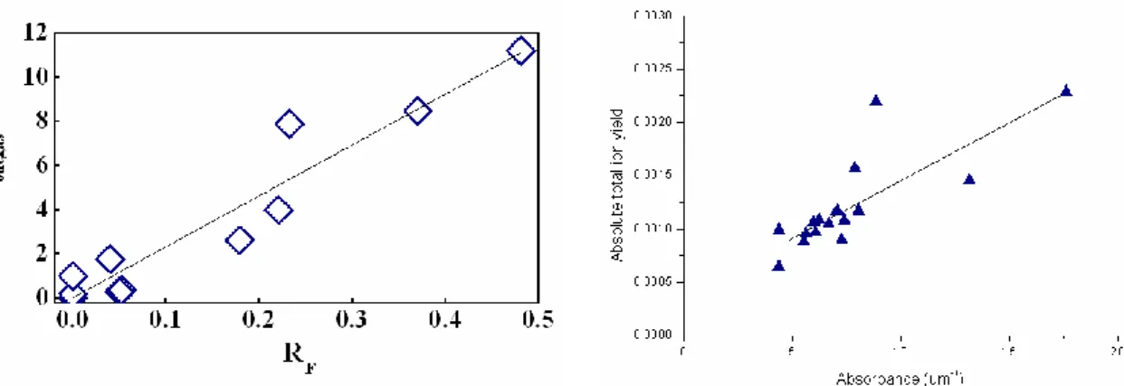
以進行相關研究。藉由本計畫所建構的光阻釋氣評估系統,本研究發現 F+的相對釋
氣量與 F 的光吸收成正比(Fig.1)。實驗結果也發現絕對總離子釋氣率(absolute total ion
yield)其數值在 10-3的數量級,而且圖中亦呈現該值與各樣品的吸收度值(由 EUV 反
射儀測得)線性相關。這是第一次的絕對測量光吸收與總離子釋氣率線性相關的研究
成果。本研究亦是第一個以直接測量的方法測得總離子釋氣率、F+及 CH
3+的曝光動 力速率參數(Dill’s C 參數)。
(1) Design and Construction of an Evaluation Chamber for the Resist Outgassing Study In this work, we design and construct an evaluation station equipped with QMS (quadruple mass spectrometer) and double-ion chamber for both neutral/ionic outgassing measurements. We also collaborate internationally with a Japanese company, Nissan Chemical Industries, Ltd. (NCI), for the resist outgassing study under EUV irradiation. The novel outgassing study finds out the important of F+ outgassing (Fig.1). This work also accomplishes the absolute total ion yield by a double-ion chamber method (Fig.2), to our knowledge the first absolute results of ionic outgassing. By both of the QMS and double-ion chamber methods, this work directly measured the exposure kinetic constants, Dill’s parameters, of the total ionic outgassing, F+ and CH3+ outgassing. This is also the first direct measurement to determine the Dill’s C parameters.
Figure 1. The correlation between F+ outgassing
(F+outgass) and F-photoabsorption (RF).
Figure 2. The correlation between ATIY and absorbance for 17 resist and underlayer samples.
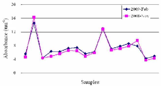
(2) 建立 EUV 波段之薄膜光學性質(nkt)量測平台 本工作延續上半年度的工作成果,進一步改進與整合相關技術,已成功建立一技 術平台以量測光阻與薄膜材料在 EUV 波段的折射係數(n),消散係數(k)與厚度(t)。 此量測平台所整合的技術能量包括 EUV 光源、高解析度反射儀、反射圖譜模擬軟體 與量測技術。透過日產化學所提供的標準試片,量測結果也與美國先進光源(ALS) 之測量結果作比較。結果顯示,計畫中建構的反射儀之角度旋轉解析度(0.0005o )符 合原計畫目標,而且與 ALS 的量測結果有極高的一致性(Fig.3)。此外,相同試片在 不同時間的量測結果也極為相近(1.080.11) (Fig.4),亦即本計畫所建立的 EUV 波段 薄膜光學性質量測平台已具有國際標準之水準,而且此平台技術已可開放提供國內 半導體產業相關廠商使用。
(2) Establish a complete nkt measurement platform @EUV for thin films
A complete and integrated nkt measurement environment @EUV, including light source, reflectometer, simulation tool and measurement technique, has been established in this project. The reflectivities of some typical samples were measured and compared with that measured at ALS (Berkeley, USA). The data show that the reflectometer’s angle precision has reached the design goal of this project. The optical properties of underlayer materials determined at NSRRC is well coherent with those measured at ALS (Fig.3). Besides, the reflectivity of the same samples measured in two different experimental runs have the refractive index values agree well with each other within (1.080.11) (Fig.4). The results indicate that the technical platform established in this project could be adapted as an international benchmark, and could be opened immediately for Taiwan’s semiconductor industry.
Figure 3. A comparison of the refractive index values determined by two institutes, ALS and NSRRC-Taiwan (this work).
Figure 4. Precision of the refractive index measurements in between runs.
2009.06~2009.11
(1) 矽基窄頻寬之 EUV 光感測器研發
由於矽材料可吸收寬頻帶的波長,截止波長約在 1.1m ,故其難以達到窄頻帶
的偵測。本研究嘗試藉由選擇適當的金屬作為閘極,以金屬-氧化層-半導體(MOS) 結構來偵測特定頻段的波長。為進行本研究工作,計畫中已建造完成一超高真空實 驗腔(Fig.1a)。實驗結果顯示,在同步輻射 EUV 光源照射下,以銀作為電極的 MOS 元件光頻譜響應峰值約在波長為 9nm 左右,此量測結果與根據電磁波理論模擬所的 的結果相近(Fig. 1b)。此閘極不只是用來讀取光電流訊號,同時也具有濾波的功能, 以選擇特定波長的光入射至矽以達成更進一步的吸收。利用簡單的金氧半結構可不 用 n 或 p 的離子佈值或擴散,且可和現今的積體電路製程整合。 5 10 15 20 25 30 35 0 . 0 0 . 2 0 . 4 0 . 6 0 . 8 1 . 0 R e s p o n s e ( a . u . ) W a v e l e n g t h ( n m ) A g 1 3 0 n m e x p S i m u l a t i o n
Figure 1. (a) Experimental Chamber for Researches of EUV Detector and Radiation Damage. (b) Measured and simulated response of the MOS tunneling photodetector with the Ag gate electrode.
(1) Si-based photo-detectors for Narrow-Band EUV Light
Due to the broad-band absorption of Si with the cut-off wavelength of ~1.1m, the narrow band detection is difficult to be realized with the Si-based photodetectors. This work attempts using appropriate gate metal to modulate the MOS (metal-oxide- semiconductor) tunneling diode for detecting specific range of light. To do that, an experimental chamber for the study of EUV MOS detector was designed and constructed
in this work (Fig.1a). Under EUV irradiation, the peak of the spectral response (@nm) of MOS tunneling photodetector with Ag electrode is close to the simulated peak of transmittance of Ag (Fig. 1b). The results indicate the gate electrode is not only used for reading out the electronic signal but also used as a filter to select the narrow band photons to enter the Si for further absorption. The MOS structure has a much simple process without dopant diffusion or implantation as compared to p-n junction and can be easily integrated with current integrated circuit.
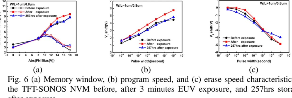
(2) 非揮發性記憶體 EUV 輻射損傷研究
本次研究針對先進的 SONOS (silicon-oxide-nitride-silicon)、NC (Nano-crystal)非揮 發性記憶體進行輻射傷害及特性變化的研究,其結構分別如圖 2 所示。該記憶體分 別作 10、20 及 30 分鐘的照射,量測記憶窗口、寫入/抹除速度、記憶力及耐久度等 記憶體性能隨著照射時間的變化。實驗結果發現,SONOS 的寫入/抹除速度在照射 後普遍劣化,照射 30 分鐘的元件經過 10 萬次的寫入抹除後,已經沒有記憶窗口(圖 3a)。相對地, NC 結構無論是記憶窗口、寫入/抹除速度、記憶力到耐久度(圖 3b) 對於照射前後皆無顯著的改變。其原因推測是因為 SONOS 以氮化矽作為電荷捕陷 層,利用單顆離散的捕陷來儲存電子,但是儲存的電子仍會在鄰近捕陷之間移動。 經過 EUV 的照射後除了產生電子電洞對,也會使氮化矽層品質變差,造成缺陷,儲 存的電子就有可能藉由這些缺陷移動,進而造成電荷的流失,使各個特性變差。而 NC 結構是將電子儲存在晶粒裡,要越過的位能高,儘管 EUV 照射產生缺陷,電子 也不易脫離原本位置而造成特性的劣化。因此,由本次實驗結果我們可以得出相較 於其他結構的記憶體,奈米晶粒非揮發性記憶體擁有良好的 EUV 輻射抵抗能力。
Fig.2 (a) Thin film transistor SONOS NVM with 4nm thick SiO2 tunneling layer 4nm, 7 nm thick Si3N4
trapping layer, and 20 nm thick SiO2 blocking layer. (b) Multi-gate TiN NC NVM with 4nm thick SiO2
tunneling layer, 7.5nm thick TiN/Al2O3 trapping layer, and 20nm Al2O3 blocking layer.
minutes.
(2) EUV Radiation damage on Non-volatile memory
The effect of EUV radiation on non-volatile memory (NVM) is studied in this work. Two advanced NVM structures, silicon-oxide-nitride-silicon (SONOS) and nano-crystal (NC), are evaluated. The device structures are shown in Fig.2. The results (Fig.3a) show that the memory performance of the SONOS NVM degrades severely after EUV exposure. In contrast, the memory window, P/E speed, and retention are not affected apparently by EUV exposure for the NC NVM as presented in Fig.3(b). The memory window dos not change after 100,000 P/E operations.
The better EUV radiation damage immunity of NC NVM than SONOS NVM can be understood by the difference in charge storage mechanism. SONOS use traps in the Si3N4 layer to store charges. EUV exposure may change the density as well as the energy level of these traps so that the memory performance changes apparently. However, for NC memory, charges are stored in NCs while the metallic NC will not be damaged by EUV, therefore, memory performance can be preserved. Based on these results, a robust design of the electronic devices can be followed for EUV lithography process.
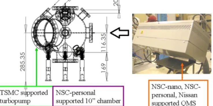
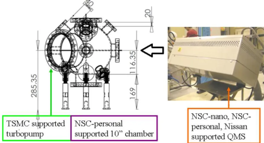
2009.12~2010.05 (1) 設計與建造一真空系統以四極質譜儀測量光阻釋氣 為了要量測絕對釋氣量,本團隊發展出一套標準作業流程以標訂釋氣的量測系 統,此流程可導出個別粒子的抽氣效率、離子壓力計的絕對量測標訂及四級質譜的 穿透效率。藉此系統參數的校正與修正,不同流量及不同種類氣體的定量相符程度 可達±20%。目前已求得初步的絕對釋氣量結果:量測標訂(benchmarking)光阻樣品 round robin resist (RRR)的釋氣量(SEMATECH 組織八個研究團量測[K. R. Dean , et al., Proc. SPIE 6519 (2007) 65191P ]),測得在 0.4 W cm-2能量密度的 EUV 光照射下之
RRR 釋氣量為 7×10¹⁵粒子/s,此數值落在標訂樣品合理的釋氣範圍內。某一底層樣 品在 IMEC 的 0.4 W cm-2 EUV 照射量下釋氣速率為 2×10¹⁴粒子/s,而本實驗室之估 計量為 1×10¹⁴粒子/s。 目前,本組人員正與 TSMC 及 NCI 合作,利用已在 IMEC 測得釋氣速率的新穎 樣品,在 NSRRC 進行標竿釋氣速率實驗。藉此,本團隊除具備光阻釋氣的基礎研究 能力外,並將在台灣建立起具世界標準光阻釋氣評估能力之設施。
(1) Design and construct an evaluation system for measuring resist outgassing with QMS
In order to count neutral outgassing in absolute numbers, we develop standard operation procedures to characterize the measurement system, the procedures of which determine the pumping speed of the system, the absolute scale of the pressure ion gauge, and the transmission function of the quadrupole mass spectrometer. The absolute gaseous throughput can be determined within ±20% consistency for various amounts of different gases using a calibrated ion gauge with their calibrated mass dependent pumping speed taken into account. Counting outgassing in real numbers has been tested preliminarily: An outgassing rate of 7×10¹⁵ molecules s-1 at 10 W cm-2 EUV density is a reasonable number
for the round-robin resist, which had been the benchmarked photoresist organized by SEMETECH and measured by eight institutes [K. R. Dean , et al., Proc. SPIE 6519 (2007) 65191P]. An underlayer material sample, of which the outgassing rate had been determined by IMEC as 2×10¹⁴ molecules s-1 at 0.4 W cm-2 EUV power density, is estimated to be ~1×10¹⁴ molecules s-1 by this work.
A benchmarking test for the absolute amount of outgassing will be conducted at NSRRC during 5/24-5/30 with the collaboration with TSMC and NCI. Samples provided by TSMC and NCI have all been measured at IMEC; therefore, in addition to the fundamental researches on resist outgassing, we are currently at the status of building the resist outgassing evaluation capability in Taiwan with the world-class standard.
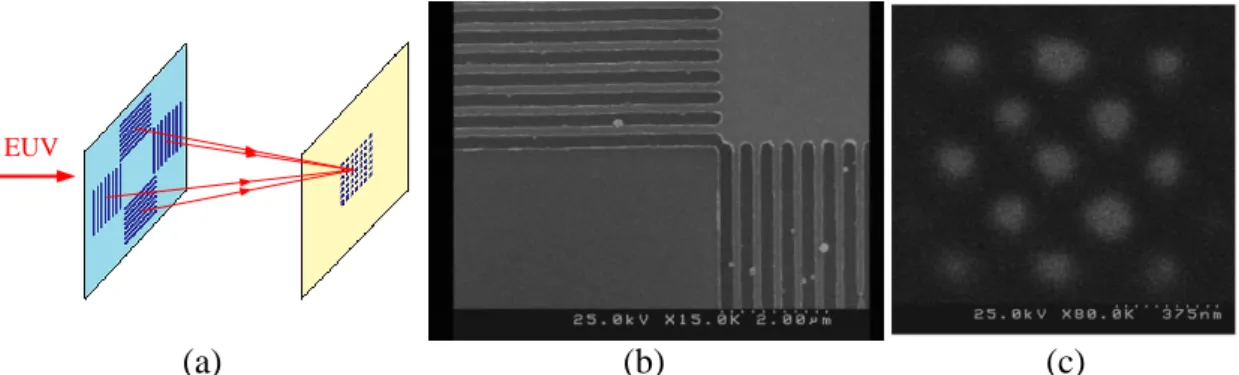
Fig. 1 A new QMS system for resist outgassing evaluation will be ready in July. Major components including a turbmolecular pump, load-lock chamber, and a 10“ measurement chamber. (2) 極紫外光干涉式曝光平台之建置 目前,極紫外光干涉式曝光平台已建置於同步輻射中心光束線 U9,可針對 15×20 mm 的試片進行曝光試驗。在穿透式繞射光柵的製作上,使用電子束微影 (Leica Weprint 200, NDL)製作 300 奈米間距,線寬與間隔 1:1 的繞射光柵。鉻光柵 層的厚度 60 奈米,一階繞射效率經計算約 5%。圖二(a)是使用電子束在光阻上定 義出的光柵圖案,(b)是經過 Lift-off 後的鉻光柵,(c)則是在 EUV 曝光後的結果, 光阻劑為 PMMA,線寬縮減至 75 奈米。二維繞射光柵是使用四道光束的干涉, 圖三(a)是四道光束干涉的示意圖。進一步製作曝光二維點陣列的穿透式繞射光 柵。圖三(b)是我們製作的繞射光柵,週期為 400 奈米。經由模擬可知,二維繞射 光柵曝光後的圖案是格子點陣列,並且間距為原光柵間距的1 2。圖三(b)是實際 曝光結果,可以發現光阻圖案上間距縮減為約 282 奈米。在未來我們將繼續進行 更小線寬的曝光試驗,目標在間距 100 奈米(干涉條紋線寬約 25 奈米)以下的光柵 製作以及曝光,並針對不同光阻劑 PMMA 及 HSQ 等尋求更佳曝光結果。
(2) Buildup of the EUV interferometric exposure platform
The EUV interferometric exposure platform has been constructed on the undulator beam-line U9 in NSRRC. Samples with a dimension of 15×20 mm can be tested. To fabricate a transmitting grating, the e-beam writer (Leica Weprint 200, NDL) has been utilized to exposure a 300 nm pitch grating pattern with 1:1 line/space. The thickness of the Cr grating is 60 nm. The 1st diffraction efficiency of the grating is
about 5% from our simulation. Fig. 2(a) shows a 300-nm pitch grating pattern exposed by e-beam lithography and Fig. 2(b) shows the Cr grating after a lift-off process. The fabricated transmission grating is then utilized as the exposing mask. The resulting exposed PMMA pattern is shown in Fig. 2(c). It’s linewidth was reduced to about 75 nm. Fig. 3(a) illustrates the scheme for the four beams exposure. We also fabricated the transmission grating for the exposure of contact/hole pattern and the Cr grating after the lift-off process is shown Fig. 3(b). The grating pitch is 400 nm. After exposure, the pitch of contact/hole pattern was reduced to 1 2 of the orginal transmission grating pitch. Fig. 3(b) shows the exposed contact/hole pattern. The pitch of the contact/hole pattern on PMMA is about 282 nm. In the future we will work on the exposure of a smaller linewidth pattern(target to 22 nm) and explore the optimal exposure condition of different photoresists such as PMMA and HSQ.
(a) (b) (c)
Fig. 2 (a) 300-nm pitch grating pattern exposed by e-beam lithography; (b) Cr grating after lift-off process; (c) EUV exposure result on PMMA.
EUV
(a) (b) (c)
Fig. 3 (a) Scheme for the four beams exposure; (b) SEM picture of 400-nm pitch diffraction grating for contact/hole pattern; (c) Exposed 282-nm pitch contact/hole pattern. (3) 設計及模擬菲涅耳波帶片極紫外光光罩檢測系統 利用純量繞射理論來模擬複合式菲涅耳波帶片在空間中或聚焦平面上的電場 強度以及光強度之分佈,進而討論傳統菲涅耳波帶片以及設計於極紫外光下的複 合式菲涅耳波帶片其聚焦特性。圖四(a)為七種不同的結構在聚焦平面上之場強 度分佈圖,七種結構皆以製程極限 50 nm 之最小線寬為考量來進行設計。由於 菲涅耳波帶片其線寬為由內往外遞減,如何穩定製程的準確度,使其達到每圈的 變化在菲涅耳波帶片的製作上是一個問題。因此,利用臺灣大學電子束實驗室之 電子束微影系統,其型號為 ELS-7500EX 的電子束直寫儀,並且使用 ZEP-520A 為電子束光阻在矽基板上進行結構製作測試,圖四(b)為線寬測試顯影之後的電 子顯微鏡相片,圖四(c)則為圖三(b)之局部放大,其右下角線寬約為 200 nm。
We use the scalar diffraction theory to simulate the field intensity and light distribution for the set of modified Fresnel zone plates. The focusing properties of traditional Fresnel zone plate and the set of modified Fresnel zone plates we proposed are compared. Fig. 4(a) shows the field intensities of seven different structures in the focal planes. We consider the line fabrication limit is 50 nm in our study. Because the line width of the Fresnel zone plate decreases from the inner zone to the outer zone, it is important to have the accuracy for each zone during the fabrication. We used ELS-7500EX electron beam system in NTU E-beam Lithography Laboratory to fabricate several structures. The photoresist is Japanese ZEON Corporation's photoresistor ZEP-520A. Fig. 4(b) is the SEM photo of the grating lines, and Fig. 4(c) is the zoom in of Fig. 4(b). The line width is about 200 nm.
(a) (b) (c)
Fig. 4 (a) The field intensities in the focal planes of seven different structures. (b) the SEM photos of the grating lines; (c) the zoom in of (b).
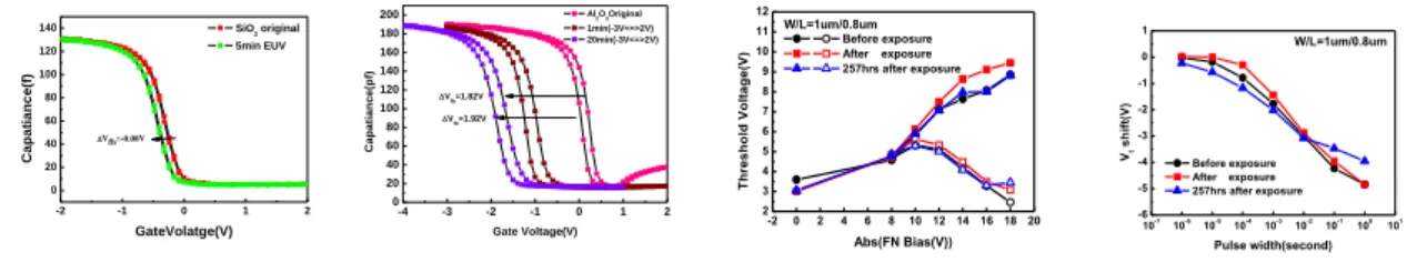
(4) 極紫外光輻射對先進非揮發性記憶體及高介電常數介電質的影響
在此高介電常數介電質的研究中,為了符合半導體產業未來的發展趨勢,探 討 EUV 輻射對金屬閘極/高介電常數介電層(High-κ dielectronic)的影響。選用氮化
鈦(TiN)為金屬閘極材料,並選用兩種介電層,分別為二氧化矽(SiO2)、氧化鋁
(Al2O3),製作成 MOS 電容器。結果顯示 SiO2的抗 EUV 輻射能力不錯(圖五),可
能和 SiO2內部的電洞缺陷密度以及吸收 EUV 的效率有關。
另一部份是探討 EUV 輻射對非揮發性記憶體的影響。本次研究針對先進的 TFT-SONOS、多閘極氮化鈦(TiN)奈米晶粒非揮發性記憶體進行輻射傷害及特性變 化的研究。SONOS NVM 元件結構為 SiO2(4nm)/Si3N4(7nm)/SiO2(20nm)。NC NVM 元件結構為 SiO2(4nm)/ TiN+Al2O3(7.5nm)/Al2O3(20nm)。結果顯示 NC 結構相較於 SONOS 結構擁有良好的 EUV 輻射抵抗能力(圖六)。
(4) Effect of Extreme Ultra-Violate Radiation on Advanced Non-volatile Memories and High Dielectric Constant Dielectrics
In the first part, EUV radiation damage on high dielectric constant (high-k) dielectric is evaluated. According to the trend of IC industry, TiN is selected as the metal gate electrode. Two kinds of high-k dielectric are evaluated. They are SiO2 and Al2O3. Among these two kinds of high-k dielectric, SiO2 exhibits the best EUV resistance. (Fig. 5) These observations indicate that SiO2 has the strongest immunity to EUV radiation damage, which may be due to less hole traps in the dielectric and the
In the second part, the impact of EUV radiation on non-volatile memory (NVM) is evaluated. Two advanced NVM structures, thin film transistor (TFT)-silicon-oxide-nitride-oxide-silicon (SONOS) and multi-gate TiN nano-crystal (NC) are used to study the variation of memory characteristics after EUV exposure. According to the experimental results, NC NVM exhibits much better EUV radiation tolerance than SONOS NVM (Fig. 6).
-2 -1 0 1 2 0 20 40 60 80 100 120 140 C a p a ti a n c e (f ) GateVolatge(V) SiO2 original 5min EUV Vfb=-0.08V -4 -3 -2 -1 0 1 2 0 20 40 60 80 100 120 140 160 180 200 C a p a ti a n c e (p f) Gate Voltage(V) Al2O3Original 1min(-3V<=>2V) 20min(-3V<=>2V) V fb=1.92V Vfb=1.82V -3 -2 -1 0 1 2 3 4 1E-13 1E-12 1E-11 1E-10 1E-9 1E-8 1E-7 1E-6 1E-5 1E-4 D ra in c u rr e n t( A ) Gate Voltage(V) initial sio2 after 2hr light sio2 after 2hr light 21hr sio2 after 2hr light 213hr
-1 0 1 2 3 4 1E-15 1E-14 1E-13 1E-12 1E-11 1E-10 1E-9 1E-8 1E-7 1E-6 1E-5 1E-4 D ra in C u rr e n t( A ) Gate Voltage(V) Al2O3after 30min light Original
(a) (b) (c) (d)
Fig. 5 C-V characteristics of the capacitors with (a) SiO2, (b) Al2O3 and .Id-Vg characteristics of the MOSFET with (c) SiO2, (d) Al2O3 dielectric before and after EUV exposure. -2 0 2 4 6 8 10 12 14 16 18 20 2 3 4 5 6 7 8 9 10 11 12 W/L=1um/0.8um Before exposure After exposure 257hrs after exposure T h re s h o ld V o lt a g e (V ) Abs(FN Bias(V)) 10-7 10-6 10-5 10-4 10-3 10-2 10-1 100 101 0 1 2 3 4 5 6 7 W/L=1um/0.8um Before exposure After exposure 257hrs after exposure Vt s h if t( V ) Pulse width(second) 10-7 10-6 10-5 10-4 10-3 10-2 10-1 100 101 -6 -5 -4 -3 -2 -1 0 1 W/L=1um/0.8um Before exposure After exposure 257hrs after exposure Vt s h if t( V ) Pulse width(second) (a) (b) (c)
Fig. 6 (a) Memory window, (b) program speed, and (c) erase speed characteristic of the TFT-SONOS NVM before, after 3 minutes EUV exposure, and 257hrs storage after exposure.
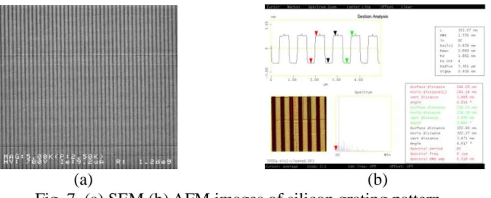
(5) 極紫外光微影術與其他微影方法的混搭與匹配
本子計畫的目的在於發展 EUVL 與其他微影方法的混搭與匹配,以降低 EUVL 之成本,並提高其效率。去年已提出 I-line 與 e-beam 微影技術的對準, 在本報告中,說明有關於以 I-line 曝光技術製作大面積格柵圖案、以 HSQ 光阻 與微縮製程所製作的奈米圖案以及兩種電子束微影圖案對準之進展,作為與 EUVL 混搭之參考。在 I-line 曝光技術方面,先以 JEOL 製作光罩,經由顯影及 TCP 電漿蝕刻後,可製作出深度約 5 nm, 寬度與週期為次微米,長度達數公分 的矽格柵結構,如圖七所示。此結構將提供同步輻射光源相關研究之使用。
(5) Mix/Match lithography with EUVL
In this subproject our goal is to develop mix-and-match processes between EUVL and other lithography methods to reduce the cost and improve the efficiency of EUVL. We have demonstrated the overlay between I-line and e-beam pattern last year. Here we report the recent progress including large area grating pattern by I-line exposure, ~15 nm line generated by electron beam lithography, and the overlay between two e-beam processes. For I-line stepper, we use JEOL e-beam to fabricate
the mask for following exposure. After development and TCP plasma etching, silicon grating made of 5 nm depth with submicron pitch and several centimeters in length was created, as shown in Fig. 7. This grating pattern has been provided to NSRRC for further study.
(a) (b)
Fig. 7. (a) SEM (b) AFM images of silicon grating pattern.
2010.06~2010.11 根據第二年計畫目標,本年度主要的研究成果包括: (1).建立一真空系統以四極 質譜儀測量光阻釋氣系統以量測絕對釋氣量 (圖 1),並發展出一套分析方法可分別 導出個別粒子的抽氣效率、離子壓力計的絕對量測標訂及四級質譜的穿透效率。目 前,本計畫正與 TSMC 及 NCI 合作,利用已在 IMEC 測得釋氣速率的新穎樣品,在 NSRRC 進行標竿(benchmarking)釋氣速率實驗,以期在台灣建立起具世界標準光阻 釋氣評估能力之設施。(2).設計與建立極紫外光干涉式曝光平台,利用同步輻射 EUV 光源,藉由穿透式光柵光罩,成功產生奈米級之 1D 與 2D 干涉圖形 (圖 2)。TSMC 亦參予本研究,協助製作 45nm 線寬之光柵,以產生更小的奈米圖形。本技術平台的 建立極有助於新微影技術與材料的研究與開發。(3).設計及模擬菲涅耳波帶片極紫外 光光罩檢測系統。本研究利用純量繞射理論來模擬複合式菲涅耳波帶片(Fresnel zone plate)在空間中或聚焦平面上的電場強度以及光強度之分佈,進而討論傳統波帶片以 及設計於極紫外光下的複合式菲涅耳波帶片其聚焦特性(圖 3)。本研究成果可最為未 來 EUV 光罩檢測技術的基礎。(4).極紫外光輻射對先進非揮發性記憶體及高介電常 數介電質的影響。研究結果顯示,高能量 EUV 光源照射將對多數半導體材料產生影 響,但是透過適當的結構與材料設計,則可以有效的提升奈米元件的 EUV 輻射抵抗 能力(圖 4)。
According to the plan, the major achievements of the 2nd-year project are: (1). Design/construct a resist evaluation system with QMS to measure the absolute outgassing under EUV irradiation (Fig.1). An analytical methodology was also developed to figure out the pumping rate of individual molecules and the penetration efficiency of the QMS. Based on a benchmarking sample, we are now cooperated with TSMC, NCI and IMEC to establish a worldwide measurement standard of resist outgassing. This is very valuable for the domestic companies to communicate with the worldwide semiconductor industrials. (2). This project also successively establishes a platform for EUV interference lithography.
Using the synchrotron EUV light source, 1D and 2 D interference pattern were generated through the home-made transmission grating mask (Fig.2). TSMC also join this work, helping to make the grating mask with 45 nm linewidth, to generate smaller pattern down below 22 nm. The platform of EUV interference lithography is very precious for studying new resist materials and new lithography technology. (3). Design/simulation of the Fresnel zone plate for EUV mask inspection system. Based on scalar theory, this work simulates the distribution of electrical field and optical intensity in the space after a compound zone plate (Fig.3), and then discusses the features of using the zone plate in the mask inspection system. (4). The effects of EUV radiation damage on the nano devices and materials. Our results indicate that high-energy EUV photons will damage most materials; however, the radiation-damage resistance of the nano devices can be effectively improved by optimizing materials and structure design (Fig.4).
Fig.1 A new QMS system for resist outgassing evaluation will be ready in July. Major components including a turbmolecular pump, load-lock chamber, and a 10“ measurement chamber.
75 nm 75 nm
283 nm 283 nm
Fig. 2 (a) Scheme for the four beams exposure; (b) SEM picture of the 1D and 2D interference- lithographed pattern.
(b)
(a)
(c)
(b)
Fig. 3 (a) The field intensities in the focal planes of seven different structures. (b) the SEM photos of the grating lines; (c) zoom in of (b).
-2 -1 0 1 2 0 20 40 60 80 100 120 140 C a p a ti a n c e (f ) GateVolatge(V) SiO 2 original 5min EUV Vfb=-0.08V -4 -3 -2 -1 0 1 2 0 20 40 60 80 100 120 140 160 180 200 C a p a ti a n c e (p f) Gate Voltage(V) Al2O3Original 1min(-3V<=>2V) 20min(-3V<=>2V) Vfb=1.92V Vfb=1.82V -2 0 2 4 6 8 10 12 14 16 18 20 2 3 4 5 6 7 8 9 10 11 12 W/L=1um/0.8um Before exposure After exposure 257hrs after exposure T h re s h o ld V o lt a g e (V ) Abs(FN Bias(V)) 10-710-6 10-510-410-3 10-2 10-1 100 101 -6 -5 -4 -3 -2 -1 0 1 W/L=1um/0.8um Before exposure After exposure 257hrs after exposure Vt s h if t( V ) Pulse width(second)
Fig. 4 C-V characteristics of the capacitors with (a) SiO2, (b) Al2O3 before and after EUV exposure. (c)
Memory window and (d) erase speed characteristic of the TFT-SONOS NVM before, after 3 minutes EUV exposure, and 257hrs storage after exposure.
2010.12~2011.07 根據第三年計畫目標,目前主要的研究成果包括: (1)利用本計畫所建立的四極 質譜儀測量光阻釋氣系統以量測絕對離子釋氣量。本研究正與TSMC及NCI合作,利 用已在IMEC測得釋氣速率的新穎樣品,在NSRRC進行標竿(benchmarking)釋氣速率 實驗。結果顯示,本研究之創新分析方法不但顯現傳統方法所得之結果,且能更靈 敏的檢測微量的光化學行為(圖1)。(2)利用本計畫所設計/建立之極紫外光干涉式曝光 平台,藉由同步輻射EUV光源與穿透式光柵光罩,成功產生奈米級之1D與2D干涉圖 形 (圖2),目前已進一步將干涉微影解析度提升至40奈米(half-pitch) (圖2),但微影參 數仍待進一步微調。(3)極紫外線投射微影系統需要仰賴反射式光學元件和光罩以斜 射照明在光阻上成像,常導致圖形偏移和線寬(CD)偏差。本計畫提出一個完全以模 型為主的修正方法,使用嚴密的三維(3D)光罩模擬整合自行提出的光學鄰近修正 (OPC)運算法,成功同時補償遮蔽與鄰近效應。(4)有關極紫外光輻射對先進非揮發性 記憶體及高介電常數介電質的影響,本年度研究結果顯示,介面層品質對於抗輻射 能力極為關鍵。而透過適當的製程方法與參數控制介面層材料品質,則可以有效的 提升奈米元件的EUV輻射抵抗能力(圖4)。
According to the plan, the major achievements of the 3nd-year project are: (1) Design/construct a resist evaluation system with QMS to measure the absolute outgassing under EUV irradiation. An analytical methodology was also developed to figure out the pumping rate of individual molecules and the penetration efficiency of the QMS. Based on a benchmarking sample, we are now cooperated with TSMC, NCI, and IMEC to
establish a worldwide measurement standard of resist outgassing. The results indicated that this novel technique has better analytical sensitivity than the traditional methods (Fig.1). That will benefit to probe the photochemical behavior of resist in more details. (2) This project has also successively established a platform for EUV interference lithography (IL). Using the synchrotron EUV light source, 1D and 2 D interference pattern were generated through the home-made transmission grating mask (Fig.2). The IL resolution has been improved from 75nm to 40 nm. However, the lithography process has still to be refined. (3) EUVL rely on reflective optical elements and masks with oblique illumination for image formation on a photoresist. It always leads to pattern shift and critical dimension (CD) bias. A fully model-based correction flow has been developed in this project, and this method can successively compensate for shadowing and proximity effects simultaneously. (4) The effects of EUV radiation damage on the nano devices and materials. Our results indicate that the oxide interface is very critical with the EUV radiation damage of the device. The radiation damage resistance of the nano-device can be effectively improved via controlling the material properties of the oxide interface (Fig.4).
Fig.1 N-2 outgassing measured by this work (blue) and IMEC (red).
Fig. 2 SEM images of (a) the transmitting diffraction grating structure and (b) EUV-IL interference fringe.
Observed gate region in plot (b) gate region Observed in plot (b)
Fig. 3 Comparison of printed patterns that were corrected by the two correction flows: (a) the type-2 6T-SRAM cells and (b) the pull-down nMOSFET gate region.
Fig. 4 C-V characteristics of the samples with different interfaces after EUV exposure (dose: 275
mJ/cm2).
6. 上述重大研究突破,與國際上類似領域之比較:
2008.08~2008.11
在此計畫的第一階段,我們已經建立了一套可用在極紫外光區段的光阻與薄膜 nkt 量測的技術平台,其中包括了一台自製的反射計,其解析度可與其他國際性的實 驗室相比,如美國的 ALS(advance light source)或是日本的 New SUBARU。因為目前 沒有可用在處理極紫外光反射率資訊的商業軟體,我們也發展一套作為曲線近似 nkt 量測結果之模擬軟體。在圖三中顯示一片基準膜的量測結果,可看出此結果相當接 近於另外二家國際性的實驗室所量測得的結果,此結果已經被一家國際性的光阻製 造公司所肯定。
In the first stage of this project, we have established a technology platform for nkt measurement of the resist and thin film in the EUV region. This achievements include a home-made reflectometer with a resolution comparable with the international laboratories such as ALS (advance light source) at USA or New SUBARU at Japan. Since there is no commercially available software for processing EUV reflectivity data, we also develop a
The measurement results of a benchmark film (Fig.3) indicate that the results are quite close to that measured by other two international laboratories. This result has been recognized by an international resist company.
2008.12~2009.05 在第一年計畫中,我們已根據計畫目標設計並建造一配備四極質譜儀與雙離子 腔之超高真空實驗系統光阻釋氣評估系統。藉由該全新的檢測方法,不但證明 F+釋 氣對光阻性質的重要性,同時也是世界上第一次發現的絕對測量光吸收與總離子釋 氣率的線性關係,以及第一次直接測量曝光動力速率 Dill’s C 參數。此光化學的動態 量測結果對於 EUV 新光阻的研發極具價值。 此外,本計畫也成功建立一技術平台以量測光阻與薄膜材料在 EUV 波段的折射 係數(n),消散係數(k)與厚度(t)。該量測平台的解析度(0.0005o )不但符合原計畫目標, 也有非常不錯的再現性(1.080.11)。特別是相同試片的分析結果與美國先進光源 (ALS)的量測結果有極高的一致性,顯示本計畫所建立的 EUV 波段薄膜光學性質量 測平台已具國際水準。 而在矽基窄頻寬之 EUV 光感測器研發中,本計畫嘗試藉由選擇適當的金屬作為閘 極同時提供濾波功能,成功地以金屬-氧化層-半導體(MOS)結構來偵測特定頻段的波 長。此元件不但結構簡單,且可和現今的積體電路製程整合。
In the first year of the project, we have designed and constructed an evaluation station equipped with QMS (quadruple mass spectrometer) and double-ion chamber for both neutral/ionic outgassing measurements. With the novel measurement scheme, we found the first time that the F+ outgassing is proportional to the F photoabsorption of the resist under EUV irradiating. The exposure kinetic rate constants, Dill’s C parameters, of the total ion, F+, and CH3+ outgassing were also determined directly. To our knowledge, this is also the first direct measurement to determine the Dill’s C parameters. The kinetic measurement results are very precious for new resist development.
A complete and integrated nkt measurement environment @EUV has been established in this project. The system not only revealed adequate angle resolution and measurement reproductivity, its measurement results is also well coherent with those taken at ALS (Berkeley, USA). These results indicate that the established technical platform could be adapted as an international benchmark for domestic industry.
In the research of EUV detector, this work attempt using appropriate gate metal as a filter, and successively modulate the MOS (metal-oxide- semiconductor) tunneling diode for detecting specific range of light. This MOS device is easily to be fabricated, and can be easily integrated with current integrated circuit compared with conventional devices.
在矽基窄頻寬之 EUV 光感測器研發中,本計畫嘗試藉由選擇適當的金屬作為閘極 同時提供濾波功能,成功地以金屬-氧化層-半導體(MOS)結構來偵測特定頻段的波 長。此元件不但結構簡單,且可和現今的積體電路製程整合。 至於在非揮發性記憶體 EUV 輻射損傷的研究結果發現,高能量的 EUV 光源可能對 電子元件產生破壞,但藉由適當的元件結構與材料設計,(例如奈米晶粒(NC)非揮發 性記憶體) 則可提供良好的 EUV 輻射抵抗能力,此研究成果對於未來在極紫外光微 影製程下的元件設計提供極有價值應用基礎。
Due to the broad-band absorption of Si with the cut-off wavelength of ~1.1m, the narrow band detection is difficult for Si-based photodetectors. This work use appropriate gate metal as a filter, and successively modulate the MOS (metal-oxide-semiconductor) tunneling diode for detecting specific range of light. The MOS structure has a much simple process without dopant diffusion or implantation as compared with p-n junction. The MOS EUV photodetector also can be easily fabricated with current semiconductor technology.
The experimental results also indicate that the high-energy EUV photons will damage the electronic devices. However, the device performance can be successively preserved via adequate design of the device structure and material. The results provide a precious basis for the device design for EUVL fabrication.
2009.12~2010.05 在過去的兩年中,本團隊致力於離子物質的釋氣研究,也提出 EUV 光化學的曝 光動力學機制,並發展出 EUV 反射儀法用來評估薄膜樣品的穩定及完整性。在台積 電的 JDP 中,確認某些光阻會有高質量的釋氣碎片,這是 TSMC 與 IMEC 合作成果 中未被鑑定出來的。當在研究 TSMC 及 NCI 的創新含矽材料時,我們觀測到材質表 面會因照光而改變其疏水性質。這個分項的基礎研究成果進而轉換成工業應用實例。 在極紫外光輻射對先進非揮發性記憶體及高介電常數介電質的影響方面,本次 研究針對先進的 TFT-SONOS、多閘極氮化鈦(TiN)奈米晶粒非揮發性記憶體進行輻 射傷害及特性變化的研究。SONOS NVM 元件結構為 SiO2/Si3N4/SiO2,NC NVM 元 件結構為 SiO2/ TiN+Al2O3/Al2O3,結果顯示 NC 結構相較於 SONOS 結構擁有良好的
EUV 輻射抵抗能力。在高介電常數介電質的部份,研究中則發現 SiO2的抗 EUV 輻
射能力不錯。這些研究的新發現,將有助於提供下世代電子元件設計的一個好的方 向。
This work has focused on studying ionic outgassing in the past two years. We proposed the exposure kinetics of EUV photochemistry, and developed the EUV reflectometer method to determine the integrity of thin-films samples, as publications listed in item (2). In the TSMC JDP, we identified ionic outgassing at massive molecular weight, which had not been reported by IMEC; while checking innovative silicon-containing compounds provided by TSMC and NCI, we found a change in surface
hydrophilic properties by EUV irradiation. The fundamental study of this sub-project on ionic outgassing turns into industrial applications.
In the study of effect of EUV radiation on advanced non-volatile memories and high dielectric constant dielectrics. Two advanced NVM structures, thin film transistor (TFT)-silicon-oxide-nitride-oxide-silicon (SONOS) and multi-gate TiN nano-crystal (NC) are used to study the variation of memory characteristics after EUV exposure. According to the experimental results, NC NVM exhibits much better EUV radiation tolerance than SONOS NVM. On the other hand, the oxide treated as high dielectric constant dielectrics was found to exhibit the best EUV resistance. These findings could be a good guide for the design of next generation devices.
2010.06~2010.11 在第二年計畫中,我們已根據計畫目標建立一配備四極質譜儀之光阻釋氣評估 系統與分析技術。該全新的檢測方法第一次發現絕對測量光吸收與總離子釋氣率的 線性關係,以及第一次直接測量曝光動力速率 Dill’s C 參數。此光化學的動態量測結 果對於 EUV 新光阻的研發極具價值。 本計畫也成功建立極紫外光干涉式曝光平台,以產生奈米級 1D 與 2D 干涉圖形。 雖然歐美日等國均已有相近設備技術(韓國尚無),但我國半導體業卻具有主導商業量 產技術方向的實力,因此本技術平台的建立極有助於台灣新微影技術與材料的研 發。此外,目前尚無有關奈米元件的 EUV 輻射損傷的研究報告。本計畫針對極紫外 光輻射損傷的研究結果,對於未來 EUVL 實際應用於量產先進非揮發性記憶體或邏 輯元件,極具有參考價值。
In this project, we have designed and constructed an evaluation station equipped with QMS (quadruple mass spectrometer) for both neutral/ionic outgassing measurements. With the novel measurement scheme, we found the first time that the F+ outgassing is proportional to the F photoabsorption of the resist under EUV irradiating. The exposure kinetic rate constants and Dill’s C parameters were also determined directly. To our knowledge, this is also the first direct measurement to determine the Dill’s C parameters. The kinetic measurement results are very precious for new resist development.
This project also successively establishes a platform of EUV interference lithography (IL) to generate 1D and 2 D nano-pattern through the home-made transmission grating mask. Although Europe, Japan and US (not Korea) have similar technology already, But Taiwan’s semiconductor industry have the power to dominate the developing direction of mass-production technology. The established EUV IL platform will benefit the development of new resist materials and new pattern technology in Taiwan. Beside, there are very rare reports about EUV radiation damage so far. The results obtained in this project indicate that high-energy EUV photon will damage most semiconductor materials.
However, the radiation-damage resistance of the nano devices can be effectively improved by optimizing materials and structure design. The results are very valuable for the EUVL mass-production of nano devices.
2010.12~2011.07 本計畫已根據計畫目標建立一配備四極質譜儀之光阻釋氣評估系統與分析技 術,該全新的檢測方法第一次發現絕對測量光吸收與總離子釋氣率的線性關係,以 及第一次直接測量曝光動力速率 Dill’s C 參數。此光化學的動態量測結果對於 EUV 新光阻的研發極具價值。 本計畫也成功建立極紫外光干涉式曝光平台,以產生奈米級 1D 與 2D 干涉圖形。 雖然歐美日等國均已有相近設備技術(韓國尚無),但我國半導體業卻具有主導商業量 產技術方向的實力,因此本技術平台的建立極有助於台灣新微影技術與材料的研 發。此外,目前尚無有關奈米元件的 EUV 輻射損傷的研究報告。本計畫針對極紫外 光輻射損傷的研究結果,對於未來 EUVL 實際應用於量產先進非揮發性記憶體或邏 輯元件,極具有參考價值。
In this project, we have designed and constructed an evaluation station equipped with QMS (quadruple mass spectrometer) for both neutral/ionic outgassing measurements. With the novel measurement scheme, we found the first time that the F+ outgassing is proportional to the F photoabsorption of the resist under EUV irradiating. The exposure kinetic rate constants and Dill’s C parameters were also determined directly. To our knowledge, this is also the first direct measurement to determine the Dill’s C parameters. The kinetic measurement results are very precious for new resist development.
This project also successively establishes a platform of EUV interference lithography (IL) to generate 1D and 2 D nano-pattern through the home-made transmission grating mask. Although Europe, Japan and US (not Korea) have similar technology already, But Taiwan’s semiconductor industry have the power to dominate the developing direction of mass-production technology. The established EUV IL platform will benefit the development of new resist materials and new pattern technology in Taiwan. Beside, there are very rare reports about EUV radiation damage so far. The results obtained in this project indicate that high-energy EUV photon will damage most semiconductor materials. However, the radiation-damage resistance of the nano devices can be effectively improved by optimizing materials and structure design. The results are very valuable for the EUVL mass-production of nano devices.
7. 評估主要成果之價值與貢獻度:
2008.08~2009.05