國 立 交 通 大 學
電子工程學系 電子研究所
碩 士 論 文
橫向擴散的射頻金氧半場效電晶體之特性
分析與模型建立
Characterization and Modeling of RF LDMOS
研 究 生 :高 誌 陽
指導教授 :張 俊 彥 院士
橫向擴散的射頻金氧半場效電晶體之特性
分析與模型建立
Characterization and Modeling of RF LDMOS
研究生:高 誌 陽 Student: Chih-Yang Kao
指導教授:張 俊 彥 院士 Advisor: Dr. Chun-Yen Chang
國立交通大學
電子工程學系 電子研究所
碩士論文
A Thesis
Submitted to Department of Electronics Engineering and
Institute of Electronics
College of Electrical and Computer Engineering
National Chiao Tung University
In Partial Fulfillment of the Requirements
For the Degree of Master
in
Electronics Engineering
July 2009
Hsinchu, Taiwan, Republic of China
中華民國九十八年七月
橫向擴散的射頻金氧半場效電晶體之特性分析與模型建立
研究生:高 誌 陽 指導教授:張 俊 彥 院士
國立交通大學
電子工程學系 電子工程所碩士班
中文摘要
近年來,射頻橫向擴散金氧半場效電晶體(RF LDMOS)在手機
基地台中,作為功率放大氣得重要元件。為了能符合新一代通訊標準
的需求,必須不斷地改善
LDMOS 的特性。在本論文中,我們將探討
四種結構:fishbone、square、octagon 和 circle 的直流、高頻和射頻
功率特性。為了得到較低的汲極電阻,我們採用了不同於傳統結構的
三種「環狀」結構。除此之外,為了抑制
square 結構所附帶角落的影
響,我們將四方形的環修正為八角形和圓形的環。另外,還針對
square
結構,去探討不同通道寬度的影響,得知通道較小的元件具有較佳的
直流表現,但是,在高頻部分則呈現較差的結果。為了進一步地了解
元件參數對高頻特性的影響,我們建立了小訊號等校電路,將其參數
萃取出並分析比較。實驗結果顯示,我們所設計的環狀結構,透過汲
極面積的增加,能夠有效地降低汲極端的寄生電阻,因而改善元件的
截止頻率(
fT
)和最大震盪頻率(
f
max)。此外輸出功率、功率增益以
及附加功率效率均有較佳的表現,而線性度和崩潰電壓則和
fishbone
結構不相上下。使用
circle 結構可以得到較大的電流和轉導,因為能
更有效地減少汲極端寄生電阻。由於
circle 結構只更動光罩之設計,
至程流程並無改變,因此實為一大優點。
另一方面,我們也完整的分析元件的電容特性。由於
LDMOS 的
通道為非均勻摻雜且具有漂移區,因此電容會有峰值產生。我們發現
square 結構會出現第二個峰值,而 circle 結構則和 fishbone 結構一樣
只有單一峰值。這是因為
square 結構再轉角處的電流密度較小,使得
電子速度需要較大的閘極偏壓才能進入類飽和狀態。
我們使用修改過的
MM20 模型去建立 fishbone 和 circle 結構的元
件模型,藉由使用
T-CAD 模擬軟體,得到橫向電場和空乏區的分佈。
另外得知具有
field plate 結構的元件操作在發生 quasi-saturation 下,
在漂移區中,其電場較為均勻並能使電阻降低。利用模擬的結果去修
改
MM20 模型成為一個簡單且沒有太多複雜運算的模型,能容易地
去描繪出元件的電性。利用修改過的模型去萃取出
fishbone 和 circle
結構的元件參數並比較分析,結果顯示,這些參數所表達的訊息與第
二章小訊號參數的結果相輔相成,具有相似的趨勢。因此,使用這模
型模擬不同步局設計的
RF LDMOS,所得到的 I-V 和 C-V 曲線也與
量測的電性曲線相符,確實得到精確的一致性。
Characterization and Modeling of RF LDMOS
Student: Chih-Yang Kao Advisor: Dr. Chun-Yen Chang
Department of Electronics Engineering and Institute of Electronics
National Chiao Tung University, Hsinchu, Taiwan
Abstract
RF LDMOS nowadays plays an important role in the RF power amplifier applications in base stations for personal communication systems. In order to meet the demands imposed by new communication standards, the performance of LDMOS is subject to continuous improvements. In this thesis, four types of layout structures, fishbone, square, octagon and circle were studied for DC, high-frequency, and RF power characteristics. To achieve lower drain resistance, we adopted “ring” structures in the layout design. In addition, to reduce corner effect, we modified the square ring structures to octagon and circle rings. For square structures, variation of channel widths was investigated. The device with smaller Wch shows better DC performance but shows worse RF performance. In order to determine the effect of device parameters on high-frequency characteristics more clearly, small-signal equivalent circuit was built to be analyzed. From the simulation results, the smaller drain parasitic resistance in the ring structures could be the key factor for improving fT and
fmax contrasting to fishbone structure. As for microwave power characteristics, output power, power gain and power added efficiency (PAE) were improved with a similar linearity with the same breakdown voltage. The extra areas in the drift region would
have lowered the drain parasitic resistance and improve the on-resistance. By using the circle structure, higher drain current and transconductance were shown by the reason of larger equivalent W/L and lower drain parasitic resistance comparing to square. Its reveals that the circle structure had a better performance, without altering the process flow.
In another part of this thesis, we discussed and analyzed the capacitance characteristics completely. For having a non-uniform doping channel and the existence of the drift region, CGS+ CGB and CGD exhibit a peak in LDMOS. In the square structure, the second peaks in a capacitance-voltage curve have been observed at high drain voltages for the first time. Besides, the circle structure has the same capacitance characteristics as the fishbone structure that indicates only one peak in the capacitance curve. While the corner region of the drift in the square shows lower current density than the edge region, it needs higher gate voltage to enter quasi-saturation. By increasing the gate voltage, the current in the corner region is high enough to make the velocity of electrons in the drift saturated.
The device models have been built for fishbone and circle structures by using the modified MM20. We obtain the lateral electric field distribution and the depletion distribution by using T-CAD simulated software. The device with field plate has uniform electric field and lower resistance in the drift region as device enters quasi-saturation. From the result of simulation, we modify the MM20 to a simple model. It is easier to describe the electrical characteristics of device. The extracted model parameters were also investigated for fishbone and circle structures. These parameters present the similar information as chapter 2. Therefore, this model shows an accurate description on I-V and C-V curves, and provides a good agreement between simulated and measured data for the RF LDMOS with different layout designs.
誌 謝
學期結束,代表青澀的學生時代劃下了完美的句點,歷經了兩年
碩士班的努力和奮鬥,終於得到了豐碩的成果,也留下了滿滿的回
憶。這一路來要感謝許多人,首要是我的指導教授張俊彥院士,老師
對於學術的熱忱及分析事物的觀點都深深的影響我做研究的態度。感
謝國家奈米元件實驗室研究員陳坤明博士和黃國威博士在研究上經
驗的傳承以及提供完善的實驗設備與資源,並給予我最完善的建議。
還有胡心卉學姐和陳勝杰學長在實務上不厭其煩地引導,幫助我克服
許多困難,實驗才能順利完成,因此非常感謝老師、學長和學姐的教
導。
由於我都是在 NDL 高頻元件實驗室做實驗,因此很感謝各位工程
師的鼎力協助,特別是生圳學長、佳松學長、文琳學長、國祥學長、
柏源學長、書毓學長、汶德學長、治華學長和榮彥學長,幫我解決量
測上的問題。另外還有在聯華電子上班的黃聖懿學長提供許多寶貴的
經驗。
感謝 CYC 實驗室的各位成員,每天朝夕相處,不論在課業上、實
驗以及生活上都給予莫大的幫助,感謝宗熺學長、偉仁學長、怡誠學
長、立偉學長、兆欽學長、弘斌學長、哲榮學長、貴宇學長、成能學
長和述穎學長,還有同學與學弟們耀峰、信淵、凱麟、培維和朝淦,
還有助理小姐秋梅,謝謝你們這段時間的相伴,讓我的研究生生活充
滿了歡笑與色彩,也成為一生難忘的回憶。
最後要感謝我的家人,親愛的爸爸高兆平、媽媽李蘭美,還有兩
位哥哥高誌鴻和高誌蔚,感謝你們默默的支持我,包容我,於精神和
生活上給予我最大的鼓勵與協助,讓我能無後顧之憂的完成學位,今
後,該換我為你們付出了。
高誌陽
於 新竹交通大學
二零零九年七月 夏
Contents
Chinese Abstract i
English Abstract iv
Acknowledgement vi
Contents vii
Table Captions xi
Figure Captions xii
Chapter 1 Introduction
1.1 Introduction to RF LDMOS 1
1.2 Advantages Compared to the Bipolar Technology 2
1.3 Advantages Compared to Other Materials 2
1.4 Motivation 3
1.5 Thesis Organization 4
Chapter 2 Characterization of RF LDMOS with Different Layout
Designs
2.1 Introduction 5
2.2 Device Structures 5
2.2.1 DC Characteristics 6
2.2.2 High-frequency Characteristics 7
2.2.3 RF Power and Linearity 10
Chapter 3 Characterization of RF LDMOS with Different Channel
Widths
3.1 Introduction 27
3.2 RF LDMOS with Square Structure 27
3.2.1 DC Characteristics 27
3.2.2 High-frequency Characteristics 28
3.2.3 RF Power and Linearity 30
3.3 Summary 31
Chapter 4 Capacitance Characteristics of RF LDMOS with Different
Layout Design
4.1 Introduction 41
4.2 Capacitances versus V
GSfor Fishbone LDMOS 41
4.3 Capacitances versus V
GSfor Different Layout Structures 43
4.4 Summary 43
Chapter 5 Modified MOS Model 20 (MM20) for LDMOS
5.1 Introduction 48
5.2 T-CAD Simulation 48
5.3 Modeling Strategy 49
5.4 Results and Discussion 52
5.5 Summary 53
Chapter 6 Conclusions and Suggestion
6.1 Conclusion 60
Table Captions
Chapter 2
Table 2-1 Extracted Ron and VBD for four different layout structures. 13 Table 2-2 Extracted gm, Rd Cgd and Cgs to see their effects on fT for different layout
structures. 13 Table 2-3 Individual effects of the model parameters on fT. The square device is as a reference. 14 Table 2-4 Extracted Rg, Rd, Cgd, Cgs, Cds and Cjdb to see their effects on fmax for different layout structures. 14 Table 2-5 Individual effects of the model parameters on fmax. The square device is as a reference. 15 Table 2-6 Cjdb and DNW area for four different layout structures. 15 Table 2-7 IIP3 and OIP3 for four different layout structures. 16
Chapter 3
Table 3-1 Extracted Ron and VBD for the square device with different channel widths. 32 Table 3-2 Extracted gm, Rd Cgd and Cgs to see their effects on fT for square device with different channel widths. 32 Table 3-3 Individual effects of the model parameters on fT. The square_10x40 is as a reference. 33 Table 3-4 Extracted Rg, Rd, Cgd, Cgs, Cds and Cjdb to see their effects on fmax for square device with different channel widths. 33 Table 3-5 Individual effects of the model parameters on fmax. The square_10x40 is as a reference. 34 Table 3-6 IIP3 and OIP3 for square device with different channel widths. 34
Chapter 5
Table 5-1 Extracted VFB, μch, μdr, θ3dr, Rdr and LD from modified MM20 for different layout structures. 54
Figure Captions
Chapter 2
Fig. 2-1 LDMOS layout structures: (a) fishbone, (b) square and (c) circle. 17
Fig. 2-2 Schematic cross section of an LDMOS transistor. 17
Fig. 2-3 (a) Subthreshold and (b) output characteristics of LDMOS transistors with different layout designs. 18
Fig. 2-4 RTH of LDMOS transistors with different layout design. 19
Fig. 2-5 Dependence of (a) |h21| and (b) MSG/MAG on frequency obtained from S-parameter measurements. 20
Fig. 2-6 (a) fT and (b) fmax versus gate voltage with different layout design. 21
Fig. 2-7 A simple equivalent circuit model of the LDMOS. 22
Fig. 2-8 Effects of small-signal model parameters on (a) fT and (b) fmax. 23
Fig. 2-9 The drain to body junction capacitance 24
Fig. 2-10 Output power, power gain and PAE versus input power with different layout designs. 25
Fig. 2-11 Drain current versus gate voltage with different layout designs. The input signal was biased at VGS=2.5V and the negative duty cycle of output signal was clipped by the cutoff region. 25
Fig. 2-12 Average drain current as a function of the input power with different layout designs. 26
Fig. 2-13 Output power and third-order intermodulation power versus input power with different layout designs. 26
Chapter 3
Fig. 3-1 (a) Subthreshold and (b) output characteristics of LDMOS transistors with different channel widths. 35Fig. 3-2 RTH of LDMOS transistors for square structure with different channel widths. 36
Fig. 3-3 (a) fT and (b) fmax versus gate voltage for square structure with different channel widths. 37
Fig. 3-4 Effects of small-signal model parameters on (a) fT and (b) fmax. 38
Fig. 3-5 Output power, power gain and PAE versus input power with different channel widths. 39 Fig. 3.6 Drain current versus gate voltage with different channel widths. The input
signal was biased at VGS=2.5V and the negative duty cycle of output signal was clipped by the cutoff region. 39 Fig. 3-7 Average drain current as a function of the input power with different channel widths. 40 Fig. 3-8 Output power and third-order intermodulation power versus input power with different channel widths. 40
Chapter 4
Fig. 4-1 Extracted CGS+CGB, CGD and the drain current versus gate voltage at different drain biases for the fishbone structure. 45 Fig. 4-2 Extracted CGS+CGB and CGD versus gate voltage at different drain biases for the (a) square and (b) circle structure. 46 Fig. 4-3 Extracted CDG versus gate voltage at different drain biases for the fishbone,
square and circle structure. 47 Fig. 4-4 Schematic view of layout structure and current distribution: (a) fishbone structure, (b) square structure and (c) circle structure. 47
Chapter 5
Fig. 5-1 The right figure shows the space charge distribution of LDMOS at Vg= 2.5V and Vd= 10V and the left figure shows the electric field along the channel region to drift region. 55 Fig. 5-2 The right figure shows the space charge distribution of LDMOS at Vg=
10V and Vd= 10V and the left figure shows the electric field along the channel region to drift region. 55 Fig. 5-3 The right figure shows the space charge distribution of LDMOS at Vg=
2.5V and Vd= 10V and the left figure shows the electric field along the channel region to drift region. 56 Fig. 5-4 The right figure shows the space charge distribution of LDMOS at Vg=
10V and Vd= 10V and the left figure shows the electric field along the channel region to drift region. 56 Fig. 5-5 Measured (mark) and simulated (line) drain current (IDS) versus gate voltage at different drain biases for the (a) fishbone and (b) circle structures. 57 Fig. 5-6 Measured (mark) and simulated (line) drain current (IDS) versus drain
voltage at different gate biases for the (a) fishbone and (b) circle
structures.. 58 Fig. 5-7 Measured (mark) and simulated (line) CGS+CGB and CGD versus gate
voltage at different drain biases for the (a) fishbone and (b) circle structures. 59
Chapter 1
Introduction
1.1 Introduction to RF LDMOS
In our life, the power device is used in many electronic products. The Lateral-Diffused MOS (LDMOS) transistor is one of the power devices. The LDMOS has been used in switching applications for many years. In the early 70’s, the first publication of LDMOS was demonstrated in microwave operation, and with technology development the LDMOS operating frequency entered into the GHz range gradually, which covered the frequency range of many of today's popular wireless products, like: Wireless infrastructure (GSM, EDGE, WCDMA, and WiMAX); Broadcast; pulsed radar; industrial, scientific and material (ISM) applications; avionics and military applications [1]. Up to 2005, Si LDMOS covered about 90 percent of the high power RF amplification applications in the 2GHz and higher frequency range, according to market analyst company Yole Développement. For more convenient life, the wireless infrastructure requiring RF power amplification is gradually built in the modern city, and the power amplifiers have to be low cost, high efficiency, and good linearity [2]. LDMOS technology plays an important role in the RF power amplifier applications in base stations for personal communication systems for frequencies up to 2.14 GHz. However it is possible, and demonstrated, to use LDMOS for frequencies up to 3.8 GHz with the latest LDMOS technology development [3]. Moreover, LDMOS transistors for amplifier applications has gone through a great development with improvements in available output power, power gain, power added efficiency and linearity together with improvements in hot carrier reliability and thermal resistance in last five years [4]. And the LDMOS technology can be incorporated in CMOS process, it is very important for power integrated circuits.
1.2 Advantages Compared to the Bipolar Technology
The advantages of using LDMOS for high power high frequency applications are on the following points:
High linearity: the process controlled short channel length makes the device works in velocity
saturation. The linear relation of drain current and gate voltage leads to a constant transconductance and improves the linearity.
Higher gain: the power gain can be improved by the lower source inductance and lower
feedback capacitance. The former can be done by tying the source and P-body together to the RF ground. In bipolar, the backside collector requires insulating from the ground and the top side emitter needs bond wire to connect to the ground. The additional bond wire introduces high inductance and limits the power gain. Also, the LDMOS is a lateral structure device which has lower feedback capacitance compared with a bipolar transistor. In addition, the LDMOS has negative temperature coefficient and does not need ballast resistor which used in bipolar and degrade the bipolar’s power gain. Therefore, the LDMOS provides higher gain than bipolar for the same output power level. This means that less amplifier stages are needed, and thus gives higher reliability and lower cost.
Thermal stability: LDMOS has no thermal runaway problem due to its negative temperature
coefficient. The higher drain current leads to higher temperature which lowers the channel mobility and resulting in a drop in drain current. On the other hand, the temperature coefficient in bipolar is positive and more prone to thermal runaway
High ruggedness: LMODS has positive temperature coefficient of channel resistance and high
drain-source breakdown voltage. Consequently, LDMOS has excellent ruggedness into an output mismatch VSWR typically 10:1 whereas the bipolar can only accept 3:1 [5-6].
1.3 Advantages Compared to Other Materials
GaAs and wide bandgap materials: SiC and GaN. GaAs based power devices can achieve higher drain efficiency and linearity due to a higher electron mobility and higher saturation velocity then silicon. However, the fact is that the saturation velocity for GaAs decreases and can be comparable to the saturation velocity for silicon at high electric field. And the lower thermal conductivity (~ 0.46 W/cm K) of GaAs is disadvantage to the high power final stage amplifiers which is needed in base station transmitters. The wide bandgap materials: SiC and GaN, which have good material properties and obtain high electric breakdown voltage and high saturation velocity. The problem for SiC is the possibility to manufacture defect free substrates. However with device continuous scaling down, silicon technology can keep playing an important role in RF systems due to reduced cost compared to other compound materials under equivalent performance. In order to compete with silicon and GaAs, the GaN and SiC have to get right way to overcome high cost. After all a superior technology must be cost competitive [7]. For silicon LDMOS, high thermal conductivity (~ 1.5 W/cm K) and quite high operation voltage make this technology suitable for base station power amplifier.
1.4 Motivation
With process technology development, the device is going to small size by reducing gate length. And power device also scales down the gate length and the drift length to improve on-resistance and transconductance. However, there is a limit of scaling down due to high-voltage on working. The choice of on-resistance and breakdown voltage is a trade-off in the conventional LDMOS. Several researchers have proposed solutions to these trade-offs such as using a double-doped offset [8], or a stacked or step drift region [9], or even the strain structure [10], or changing the process flow. There is also other solution to solve the trade-off between the on-resistance and breakdown voltage by optimizing the layout design. In this thesis, four types of layout structures (fishbone, square, octagon and circle) were studied for DC, high-frequency, and RF power characteristics. According to its structure, the parasitic
drain resistance of the LDMOS becomes more important than that of the conventional MOSFET for the present drift region. In order to effectively use layout area and reduce the parasitic effect from metal connected line or device to enhance the performance of device, we have to know which parts of the device have a great influence. In addition, the device capacitances influence the input, output and feedback capacitances, which are important in the dynamic operation, and have large impact on device high-frequency performance. The capacitance characterization and modeling of LDMOS transistors have been studied widely [11-13]. Finally, an accuracy model that describes the electric characteristics of RF LDMOS is needed for circuit design. In this thesis, an LDMOS modeling technique was also investigated.
1.5 Thesis Organization
The content in this thesis includes the following parts.
Chapter 1 introduces the LDMOS for RF applications and the motivation of this thesis. Chapter 2 presents the DC, high-frequency and RF power performances of LDMOS with different layout structures. In addition, the small-signal model parameters were extracted to investigate their effects on fT and fmax.
In chapter 3, the DC, high-frequency and RF power performances of square LDMOS with various channel widths were analyzed. Also, the small-signal model parameters were extracted to investigate their effects on fT and fmax.
Chapter 4 presents the unusual capacitance behavior of RF LDMOS with fishbone, square and circle structures. Capacitance versus gate voltages with different drain voltage was investigated.
Chapter 5 presents the modified MM20 modeling for RF LDMOS. Finally, the conclusions of this thesis are summarized in Chapter 6.
Chapter 2
Characterization of RF LDMOS with Different Layout Designs
2.1 Introduction
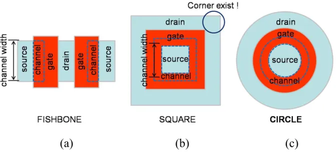
In high-power applications, the RF transistors are usually implemented in a “fishbone” structure, as shown in Fig. 2.1(a). All the gate fingers are divided into several subcells, in each of which, 2-10 gate fingers are grouped together. For RF performance concern, multi-finger layouts are used to design wide MOSFETs for reducing the gate resistance and source/drain junction capacitance. Since the gate resistance would limit the power gain attainable at a certain frequency and thus fmax [14-18]. The drain resistance which includes accumulation layer resistance and JFET resistance are the main component in LDMOS to have influence on the on-resistance. Here, in order to achieve lower on-resistance, we adopted a “square” structure which is different from the “fishbone” in the LDMOS layout design (see Fig. 2.1(b)). However, in our previous study, we found that the square structure has higher gate capacitances compared to that of fishbone structure, owing to the corner effect [19]. In order to reduce the corner effect, we modified the square ring structures to octagon and circle rings (see Fig. 2.1(c)) in this work. Then we investigated the DC, high-frequency, and RF power characteristics of the devices with different layout structures.
2.2 Device Structures
RF LDMOS transistors were fabricated using a 0.5 μm LDMOS process. The schematic cross section of the device is shown in Fig. 2.2. The drain region was extended under the gate oxide and consisted of a lightly doped N-well drift region and an N- region with higher doses for on-resistance control. The source region and the p-body were tied together to eliminate extra surface bond wires to reduce the source inductance and improve the RF performance in a power amplifier configuration [20]. The gate oxide thickness was 135 Å and the mask
channel length (LCH) was 0.5μm. The drift length (LDrift=LOV+LFOX) was 2.4μm. The fishbone structure used in this study had 10 cells which each cell had 4 fingers with finger width LF=10μm. For the other structures, the width of each gate ring was 40μm and each cell was arranged as a 5x2 array in one device. The source region was surrounded by the drain region, while the gate was located between the source and the drain (see Fig. 2.1). To compare the performance of all structures fairly, the total channel width is the same (W= 400μm).
2.2.1 DC
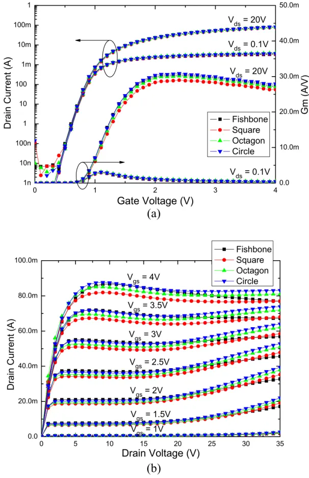
Characteristics
The I–V characteristics of the LDMOS with different layout structures are shown in Fig. 2.3. For ring structures, the circle device shows the highest drain current and transconductance than others, and the square device shows the worst performance. Because the square structure has additional four corners, where the drain current density is lower than that in edges, the effective drain resistance would be higher than that in octagon and circle structures. It results a lower drain current compared to that in other structures. The dc characteristics of fishbone device are also shown in Fig. 2.3. The drain current and transconductance are not lower than the ring structures in low- and medium-bias regions, but in high-bias region the drain current would be suppressed more due to the quasi-saturation effect. Because the fishbone structure has higher resistance in the drift region, a larger voltage drop in drift region will exist than that of ring structures. As a result, the carriers in the drift region of the fishbone device will enter the velocity saturation earlier than ring structures. When the velocity saturation in the drift region occurs, the device will operate in “quasi-saturation”, where the intrinsic MOS is still in linear operation. This effect is generally observed at high gate voltages. As the device enter the quasi-saturation, the gate control ability decreases which limits the drain current level and delays the transition between linear and saturation regime. So when the device operates at high power condition, the ring structure has a better performance due to reduced quasi-saturation effect.
From the output I–V characteristics of the fishbone structure, we observe a negative output resistance in the high-current region. With high current density in the transistor, the rise in device temperature resulted from the dissipated power becomes significant. The increased device temperature reduces the carrier mobility and saturation velocity [21]. Fig. 2.4 shows the thermal resistance (Rth) of three different layout structures. The fishbone device has higher thermal resistance compared to ring devices. Due to compact layout area, the self-heating effect in the fishbone structure is significant. The device self-heating can be improved by increasing the distance between each cell of fishbone.
The drain-source on-resistance is an important parameter for describing the performance of LDMOS transistors. The on-resistance (Ron) is extracted from the linear forward I–V characteristics at gate voltage VGS = 2.5 V, since it is predominated by the drift region under such a condition (see Table 2-1). Ron is related to the drain current and is dependent on the drain resistance. Among the ring structures, the Ron is lowest in the circle device, and it is interpreted as being due to a lowest drain resistance, In Table 2-1, we also observe that the Ron in fishbone device is lower than that in ring devices due to lower channel resistance. This result is limited by standard processing. In addition, another important parameter is breakdown voltage for LDMOS. We obtain that the four devices have the similar breakdown voltage (VBD≅ 41-43V).
2.2.2 High-frequency
Characteristics
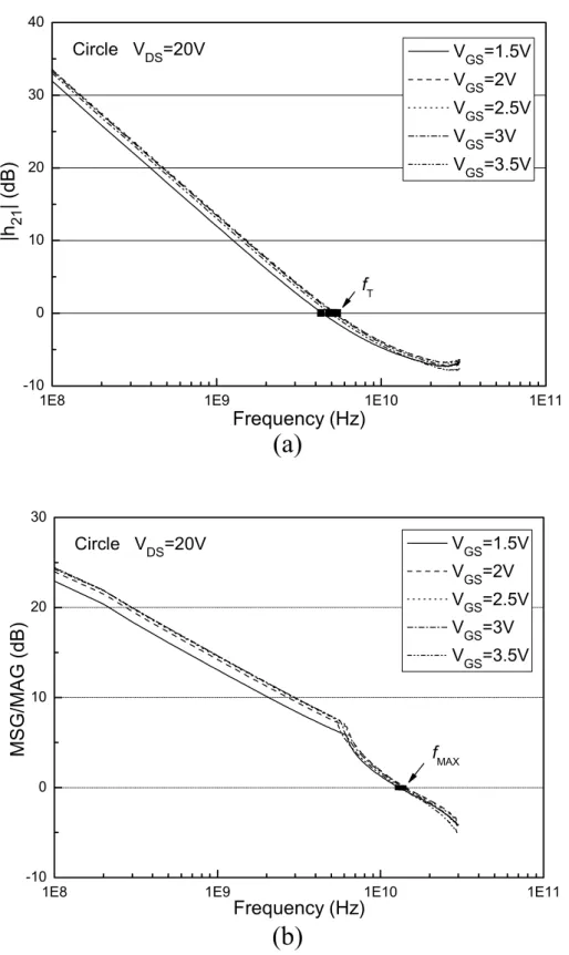
To characterize the high-frequency performance, the S-parameters were measured on-wafer from 0.1 to 30 GHz using an HP8510 network analyzer and then de-embedded by subtracting the OPEN dummy. Fig. 2.5 shows the high-frequency characteristics of circle structure. The maximum stable gain/maximum available gain (MSG/MAG) and short-circuit current gain (h21) were calculated from S parameters. The cutoff frequency (fT) and maximum oscillation frequency (fmax) were determined as the frequency where the current gain was 0 dB
and the frequency where MAG was 0 dB, respectively. The transistors were measured at drain voltage VDS=20 V with different gate voltages. From Fig. 2.6, fT had maximum values at VGS=2.5 V, where the transconductance showed a peak. With increasing the gate voltage, both
fT and fmax decreased owing to the mobility degradation and quasi-saturation effects.
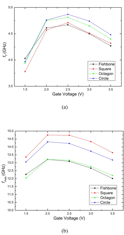
The cutoff frequency and maximum oscillation frequency for the LDMOS with different layout structures are compared in Fig. 2.6. The transistors were biased at VGS=2.5 V and VDS=20 V to obtain the maximum value of fT. It is observed that the values of fT in these layout structures are circle > octagon > square > fishbone and the values of fmax are square > circle > octagon > fishbone.
By analyzing a MOSFET small-signal equivalent circuit, we can determine the effect of device parameters on high-frequency characteristics more clearly. We adopted a simple model (shown in Fig. 2.7) and extracted the equivalent circuit parameters of the LDMOS by the method described in ref. 22. After de-embedding the extrinsic parasitic resistances and the substrate-related parameters, the intrinsic components could be directly extracted from intrinsic Y-parameters (Yi) by the following equations [23]:
,12 1 Im( ) gd i C Y ω = − 2 ,11 ,11 2 ,11 Im( ) (Re( )) (1 ) (Im( ) ) i gd i gs i gd Y C Y C Y C
ω
ω
ω
− = ⋅ + − ,22 ,12 1 Im( ) ds i i C Y Y ω = + ,11 2 2 ,11 ,11 Re( ) (Im( ) ) (Re( )) i i i gd i Y R Y ωC Y = − + ,22 1 Re( ) ds i R Y = 2 2 2 0 ((Re( ,21)) (Im( ,21) ) ) (1 ) m i i gd g g = Y + Y +ωC ⋅ +ω2C2 sRi ,21 ,21 Im( ) Re( ) 1 sin( gd i gs i i ) m C Y C R Y arc gω
ω
τ
ω
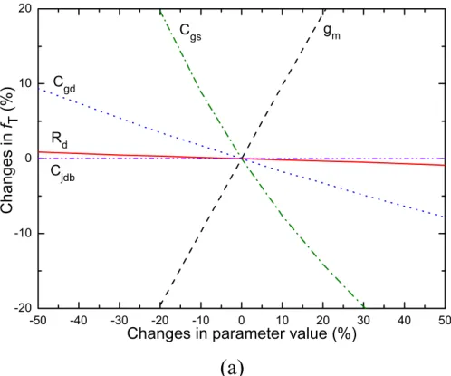
− − − =Using extracted parameters from the existing device and altering one parameter at the time, the effect of model parameters on the cutoff frequency and maximum oscillation frequency can be visualized. The influences of model parameters on fT and fmax are shown in Fig. 2.8. The x-axis showed the parameter value departure from the initial value in percent. The y-axis showed the change in frequency in percent. Parameters not shown in the figure had approximately the same value for the ring and fishbone structures or had a minor influence on
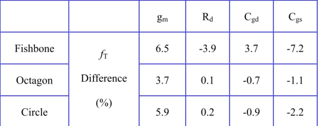
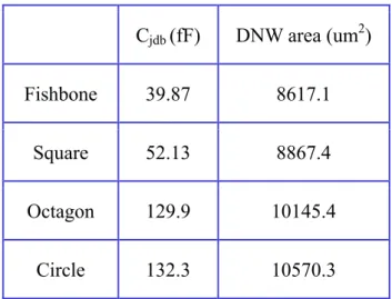
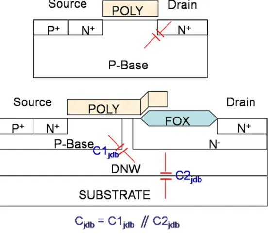
fT and fmax. As shown in Fig. 2.8(a), the intrinsic transconductance (gm), gate-source capacitance (Cgs) and gate-drain capacitance (Cgd) have large effect on fT. The cutoff frequency can be expressed in a simple way of fT = gm/ 2π (Cgs+ Cgd) which is related to the gm and input intrinsic capacitances (Cin= Cgs+ Cgd). The extracted model parameters that affect the fT more significantly are listed in Table 2-2. For ring structures, we find that the slight increase of fT in circle device is mainly due to the slight increase of gm. When gm increases from 34.58 mA/V to 35.92 mA/V and 36.7 mA/V for octagon and circle respectively contrasting with square structure, fT is improved by about 3.7% and 5.9% (see Table 2-3). The gate capacitances are nearly unchanged. For fishbone device, however, the drain resistance (Rd) is large and its effect on fT cannot be ignored. Rd represents the drain contact resistance and part of the drift region. As compared to square device, Rd has been increased from 2.6 Ω to 9.05 Ω for fishbone device, and thus fT becomes worse about -3.9%. In addition, the lower Cgd and higher Cgs in the fishbone structure cause about 3.7% and -7.2% changes in fT due to different layout design. Otherwise the intrinsic gm of fishbone is the biggest among four structures and makes fT increase about 6.5%. As illustrated in Fig. 2.8(b), in addition to the intrinsic parameters, the Rd, gate resistance (Rg), drain-source capacitance (Cds) and drain-substrate junction capacitance (Cjdb) have apparent effects on fmax [24]. The extracted model parameters that affect fmax more significantly are listed in Table 2-4. The square structure has the highest fmax due to lower parasitic drain junction capacitance (Cjdb) and gate to source capacitance (Cgs). The Cjdb can be separated into two parts; one is between P-body
and DNW, another is between DNW and substrate (see Fig. 2.9), and then the Cjdb is relative to area of DNW. Because the square structure has small area, the DNW area and thus the Cjdb are small (see Table 2-6). Contrary to square, the fishbone structure has the lowest fmax due to higher Rd and Cgs in addition to lower fT. Comparing to the square structure, the octagon and circle structures have lower fmax due to larger Cjdb and drain to source capacitance (Cds).A part element of Cds represents the overlap of metal conducting wires. Although fmax should be improved with the gm increasing, the other parameters will also affect the fmax. For ring structures, the Cds increases from 97.62 fF to 119.9 fF and 119.8 fF for octagon and circle respectively contrasting with square structure, both fmax become worse about -2.9% (see Table 2-5). In addition, the Cjdb increase from 52.13 fF to 129.9 fF and 132.3 fF, the fmax also become worse about -7.6% and -7.8%. For fishbone structure, we are easy to find the Rd has a great impact on fmax and becomes important. As compared to square device, Rd has been increased from 2.6 Ω to 9.05 Ω for fishbone device, and thus fmax becomes worse about -23.8%. In addition, the lower Cgd and higher Cgs in the fishbone structure cause about 8.6% and -6.9% changes in fmax due to different layout design. Otherwise the extrinsic parameters (Rg and Cds) also make fmax increase about 5.7% and 6.8% respectively. Consequently, the fmax for circle structure is lower than the one for square structure by about -3.5% (fmax was 14.74 GHz for the square structure and 14.22 GHz for the circle structure). The fmax for octagon structure is lower than the one for square structure by about -10.7% (fmax was 14.74 GHz for the square structure and 13.16 GHz for the circle structure). The fmax for fishbone structure is lower than the one for square structure by about -11.2% (fmax was 14.74 GHz for the square structure and 13.09 GHz for the fishbone structure).
2.2.3
RF Power and Linearity
As well as the high-frequency characteristics, the microwave power characteristics are also investigated using the load-pull measurement. In our study, the source and load
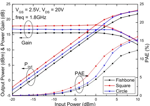
impedances were tuned for maximum power gain and maximum output power, respectively. The power tune is setup at 2 dBm before the power gain starts to degrade. For having the value of fmax in the range from 13 GHz to 15 GHz, the devices were measured at 1.8 GHz with gate bias VGS=2.5 V and drain bias VDS=20 V. Figure 2.10 shows the output power, power gain and power added efficiency (PAE) with different layout designs. There are only three layout structures of LDMOS: fishbone, square and circle, because the octagon structure is similar to circle structure.
The power gain is related to fmax. The square device has largest power gain and the fishbone device has smallest power gain (see Fig. 2.10). We find that the power gain of square structure degrades earlier than others when input power goes beyond 1-dB compression point (P1dB). The main reason for gain compression is attributed to the clipping effect. The border of output I-V curve will cause output waveform to be clipped for MESFET, PHEMT and HBT [25-27]. The clipping effect can also been found in LDMOS. Figure 2.11 shows the drain current versus gate voltage with input and output waveform for different layout designs. Part of the AC-signals on the drain current would be cut off as the input power becomes larger enough. At this condition, the average drain current increased with the increasing input power (see Fig. 2.12) and the power gain has been compressed. This is because the dynamic load line exceeds the border of DC I-V. For the square structure, the drain current makes the negative duty cycle of output waveform enter the cutoff region earlier. This indicates that the average drain current started to increase earlier (see Fig. 2.12) and the gain compression occurs prior. And another two structures have the similar characteristics that the gain compression occurs lately. Generally the device operating range is before P1dB point, so the circle has wider operating range than square. Consequently, although the square structure shows higher value of output power, power gain and PAE, the operating range is narrower slightly. Since the DC behaviors were changed, the linearity would also be affected with different layout designs. The input and output third-order intercept points (IIP3 and OIP3) for
three structures are listed in Table 2-7. As measuring IM3, the output impedance is tuned at maximum gain. The IIP3 and OIP3 are different in three structures due to different load impedance (as shown in Fig. 2.13).
2.3 Summary
LDMOS with different structures for RF applications are investigated. The ring structure has a better performance than the fishbone structure, without altering the process flow. The quasi-saturation effect is suppressed in the LDMOS with the ring structure due to lower drain parasitic resistance. In addition, the fT and fmax are also enhanced for the ring structure due to the lower drain parasitic resistance. The distance of each cell for ring structure can be reduced to improve RF performance because the self-heating effect for ring device is smaller than one for fishbone device. The circle device can improve the disadvantage of square device on DC performance due to uniform current density that reduces the drain resistance. Although the square structure shows higher value of output power, power gain and PAE, the operating range and linearity are worse than circle. Our results suggested that, using a circle structure, both better DC and RF characteristics can be achieved.
Table 2-1 Extracted Ron and VBD for four different layout structures. Ron (Ω-㎜) VBD (V) Fishbone 22.95 41 Square 24.59 42 Octagon 23.57 43 Circle 23.05 41
Table 2-2 Extracted gm, Rd Cgd and Cgs to see their effects on fT for different layout structures.
gm (mA/V) Rd (Ω) Cgd (fF) Cgs (fF) fT (GHz) Fishbone 36.9 9.05 147.2 1080 4.67
Square 34.58 2.6 185.4 986 4.71 Octagon 35.92 2.48 193.4 998.2 4.81
Table 2-3 Individual effects of the model parameters on fT. The square device is as a reference. gm Rd Cgd Cgs Fishbone 6.5 -3.9 3.7 -7.2 Octagon 3.7 0.1 -0.7 -1.1 Circle fT Difference (%) 5.9 0.2 -0.9 -2.2
Table 2-4 Extracted Rg, Rd, Cgd, Cgs, Cds and Cjdb to see their effects on fmax for different layout structures. Rg (Ω) Rd (Ω) Cgd (fF) Cgs (fF) Cds (fF) Cjdb (fF) fmax (GHz) Fishbone 1.91 9.05 147.2 1080 53.97 39.87 13.09 Square 2.43 2.6 185.4 986 97.62 52.13 14.74 Octagon 2.48 2.48 193.4 998.2 119.9 129.9 13.16 Circle 2.71 2.2 194.6 1013 119.8 132.3 14.22
Table 2-5 Individual effects of the model parameters on fmax. The square device is as a reference. gm Rg Rd Cgd Cgs Cds Cjdb Fishbone 5.9 5.7 -23.8 8.6 -6.9 6.8 2.5 Octagon 3.4 -0.7 0.8 -1.8 -1 -2.9 -7.6 Circle fmax Difference (%) 5.4 -2.9 3 -2 -2.1 -2.9 -7.8
Table 2-6 Cjdb and DNW area for four different layout structures.
Cjdb (fF) DNW area (um2)
Fishbone 39.87 8617.1
Square 52.13 8867.4
Octagon 129.9 10145.4
Table 2-7 IIP3 and OIP3 for four different layout structures.
IIP3 (dBm) OIP3 (dBm)
Fishbone 15.04 31.03 Square 12.92 30.58
(a) (b) (c)
Fig. 2.1 LDMOS layout structures: (a) fishbone, (b) square and (c) circle.
(a)
0 1 2 3 4 1n 10n 100n 1 10 100 1m 10m 100m 1 0.0 10.0m 20.0m 30.0m 40.0m 50.0m Vds = 0.1V Vds = 20V Vds = 0.1V D rain C urren t (A)Gate Voltage (V)
Fishbone Square Octagon Circle Vds = 20V G m (A /V ) 0 5 10 15 20 25 30 35 0.0 20.0m 40.0m 60.0m 80.0m 100.0m Vgs = 1V Vgs = 1.5V Vgs = 2V Vgs = 2.5V Vgs = 3V Vgs = 3.5V Dr ain Cur rent ( A )Drain Voltage (V)
Fishbone Square Octagon Circle Vgs = 4V(b)
Fig. 2.3 (a) Subthreshold and (b) output characteristics of LDMOS transistors with different layout designs.
0.0 0.2 0.4 0.6 0.8 1.0 0 10 20 30 40 50 60 70 RTH=55.59
(
oC/W)
Fig. 2.4 RTH of LDMOS transistors with different layout design.
RTH=54.81 (oC/W) RTH=78.81
(
oC/W)
VDS=20V VGS=3.5V TC= 25+RTHPD Fishbone Square Circle Tc-Ta ( o C ) Power Dissipation (W)(a)
1E8 1E9 1E10 1E11
-10 0 10 20 30 40 |h 21 | ( d B) Frequency (Hz) VGS=1.5V VGS=2V VGS=2.5V VGS=3V VGS=3.5V Circle VDS=20V fT
1E8 1E9 1E10 1E11
-10 0 10 20 30 Circle VDS=20V MS G/MAG (dB) Frequency (Hz) VGS=1.5V VGS=2V VGS=2.5V VGS=3V VGS=3.5V fMAX
(b)
Fig. 2.5 Dependence of (a) |h21| and (b) MSG/MAG on frequency obtained from S-parameter measurements.
1.5 2.0 2.5 3.0 3.5 3.5 4.0 4.5 5.0 f T (G H z) Gate Voltage (V) Fishbone Square Octagon Circle
(a)
1.5 2.0 2.5 3.0 3.5 10.0 10.5 11.0 11.5 12.0 12.5 13.0 13.5 14.0 14.5 15.0 f max (GH z) Gate Voltage (V) Fishbone Square Octagon Circle(b)
R
gR
dR
sC
gsR
iR
subR
ds=1/g
dsC
subC
gdC
dsC
jdbg
mV
gsG
D
S
0exp(
)
m mg
=
g
−
j
ωτ
Vgs
+ _-50 -40 -30 -20 -10 0 10 20 30 40 50 -20 -10 0 10 20 Cha nges in f T (% )
Changes in parameter value (%)
gm Cgs Cgd Rd Cjdb
(a)
-50 -40 -30 -20 -10 0 10 20 30 40 50 -20 -15 -10 -5 0 5 10 15 20 Cjdb Cds Rd Rg Cgd Cgs Change i n f MA X (%)Change in parameter value (%)
gm
Rsub Csub
(b)
-20 -15 -10 -5 0 5 10 -5 0 5 10 15 20 25 0 5 10 15 20 25 Ou tp ut Powe r ( d Bm) & Power G a in (dB) Input Power (dBm) Fishbone Square Circle Gain Pout PAE VGS = 2.5V, VDS = 20V freq = 1.8GHz PAE (%)
Fig. 2.10 Output power, power gain and PAE versus input power with different layout designs.
Fig. 2.11 Drain current versus gate voltage with different layout designs. The input signal was biased at VGS=2.5V and the negative duty cycle of output signal was clipped by the cutoff region.
-20 -15 -10 -5 0 5 10 30 35 40 45 50 55 60 VGS = 2.5V, VDS = 20V freq = 1.8GHz Aver age Dr ain Cur rent ( m A ) Input Power (dBm) Fishbone Square Circle
Fig. 2.12 Average drain current as a function of the input power with different layout designs.
-20 -15 -10 -5 0 5 10 15 20 -100 -80 -60 -40 -20 0 20 40 OIP3 IIP3 VGS= 2.5V VDS= 20V frequency = 1.8GHz
Output Power & IM3 (dBm)
Input Power (dBm) Fishbone Square Circle Pout IM3
Fig. 2.13 Output power and third-order intermodulation power versus input power with different layout designs.
Chapter 3
Characterization of RF LDMOS with Different Channel Widths
3.1 Introduction
The corner effect of square structure is described in chapter 2. Under fixing the drift length, we studied the corner effect by changing the channel width of a cell. Different ratios of corner areas to edge area would result in different drain parasitic resistances and capacitances [19]. Square structures with different channel widths for DC, high-frequency, and RF power characteristics are investigated.
3.2 RF LDMOS with Square Structure
The square device used in this study had different channel widths per a cell (Wch=20μm, 40μm and 100μm). For making a fair comparison, these devices had the same total channel width (W=400μm). Therefore, the cells in the these devices were arranged as 10x2, 5x2 and 2x2 arrays, respectively. These devices are named as “square_20x20”, “square_10x40” and “square_4x100”, respectively.
3.2.1 DC
Characteristics
Fig. 3.1 shows the I–V characteristics of the LDMOS with different channel widths. The device with larger Wch shows a lower drain current and transconductance. Also with a larger Wch, the higher resistance in the drift region leads to the quasi-saturation effect occurs earlier. The extracted on-resistance and breakdown voltage with various channel widths per a cell are shown in Table 3-1. The Ron is extracted from the linear forward I-V characteristics at gate voltage VGS=2.5 V and normalized to the total width. As indicated in Table 3-1, the devices with different channel widths have similar breakdown voltage. In addition, we find that, as the
channel width increases, the Ron increases due to the increase of drain series resistance. By fixing the drift length, the ratio of corner area to side area will be reduced with increasing Wch. Therefore, the device with large Wch has smaller equivalent drift width compared to the device with small Wch, leading to higher drain resistance.
From the output I–V characteristics, we observe a negative output resistance in the high-current region. With high current density in the transistor, the rise in device temperature resulted from the dissipated power becomes significant. Fig. 3.2 shows the thermal resistance (Rth) with different channel width per a cell. The device with large Wch has higher thermal resistance than that with small Wch due to compact layout area and has significant self-heating effect. The device self-heating can be improved by increasing the distance between each cell.
3.2.2 High-frequency
Characteristics
The dependences of the cutoff frequency and maximum oscillation frequency on the channel width for the LDMOS are compared in Fig. 3.3. The transistors are biased at VGS=2.5 V and VDS=20 V to obtain the maximum value of fT. It is obvious that fT and fmax both decrease with decreasing Wch due to lower parasitic capacitance. On the other word, the both values of fT and fmax in these layout devices are square_4x100 > square_10x40 > square_20x20.
By analyzing a MOSFET small-signal equivalent circuit, we can determine the effect of device parameters on high-frequency characteristics more clearly. Using extracted parameters from the existing device and altering one parameter at the time, the effect of model parameters on the cutoff frequency and maximum oscillation frequency can be visualized. The influences of model parameters on fT and fmax are shown in Fig. 3.4. The x-axis showed the parameter value departure from the initial value in percent. The y-axis showed the change in frequency in percent. Parameters not shown in the figure had approximately the same value for the square structures or had a minor influence on fT and fmax. As shown in Fig. 3.4(a), the
intrinsic transconductance (gm), gate-source capacitance (Cgs) and gate-drain capacitance (Cgd) have large effect on fT. The cutoff frequency can be expressed in a simple way of fT = gm/ 2π (Cgs+ Cgd) which is related to the gm and input intrinsic capacitances (Cin= Cgs+ Cgd). The extracted model parameters that affect the fT more significantly are listed in Table 3-2. According to above equation, we know that the fT is proportional to gm,but the measured data we obtained is reverse proportional to gm. So we confirm that the fT is relative to Cin and Cin increases with increasing the extra area of drift region. In addition, the fmax has the similar appearance. Comparing to square_10x40, as Cgd is changed from 185.4 fF to 275.7fF and 130.4 fF for square_20x20 and square_4x100, fT vary about -7.6% and 5.4% respectively (see Table 3-3). Similarly, Cgs is also changed from 986 fF to 971 fF and 994 fF for square_20x20 and square_4x100 and makes fT about 1.3% and -0.7% changes respectively. Therefore, it is obvious that the Cgd has a great effect on fT for these devices. The increasing area of drift region led to Cgd rise, and decreasing area of source led to Cgs reduce for square device. As illustrated in Fig. 3.4(b), in addition to the intrinsic parameters, the Rd, gate resistance (Rg), drain-source capacitance (Cds) and drain-substrate junction capacitance (Cjdb) have apparent effects on fmax. The extracted model parameters that affect fmax more significantly are listed in Table 3-4. The transistor has larger value of fmax with increasing channel width due to smaller Cds and Cgd. The former is relative to the overlapped area of metal conducting wires and the later is relative to the drift region area. In addition, one reason results the lowest fmax for square_20x20 is larger Cjdb. The value of Cjdb is relative to the DNW area and device area. Comparing to square_10x40, Cgd varies from 185.4 fF to 275.7 fF and 130.4 fF for the square_20x20 and square_4x100, and make fmax about -17.1% and 12.4% changes respectively (see Table 3-5). Another parameter affects fmax more is Cds. As Cds is changed from 97.62 fF to 149.9 fF and 58.32 fF for the square_20x20 and square_4x100, the fmax vary about -6.3% and 6.1% respectively. In addition, the square_20x20 and square_4x100 both have smaller Rg and cause fmax about 8.4% and 7% changes due to different cell arrangement.
The Rd also has a little effect and makes fmax about 4.7% and -5.9% changes for the square_20x20 and square_4x100. Otherwise, the larger Cjdb just in square_20x20 decreases fmax about -8.6% contrasting with square_10x40. Consequently, Comparing to square_10x40, using the square_20x20, we estimate that fmax become worse by about -16.1% (fmax was 12.37 GHz for the square_20x20 and 14.74 GHz for the square_10x40) and using the square_4x100, we estimated that fmax become better by about 6.4% (fmax was 15.68 GHz for the square_4x100 and 14.74 GHz for the square_10x40). Therefore, Cgd is the key factor for improving fT and fmax by using the square structure.
3.2.3
RF Power and Linearity
The load-pull measurement uses the same setup as chapter 2. Figure 3.5 shows the output power, power gain and power added efficiency (PAE) for square device with different channel widths. The power gain characteristic is related to fmax. The transistor with llarge Wch has larger power gain and out power but they degrade earlier when input power was larger than 1-dB compression point (P1db) (see Fig. 3.5). The main reason for gain compression is attributed to the clipping effect that is explained in chapter 2. As the channel width increase, the lower drain current makes the negative duty cycle of output waveform enter the cutoff region earlier (see Fig. 3.6). This indicates that the average drain current started to increase earlier (see Fig. 3.7) and the gain compression occurs prior. The transistor with large channel width has wider operating range that is before P1dB point. Consequently, although the square device with large channel width shows higher value of output power, power gain and PAE, the operating range is narrow slightly. Since the DC behaviors were changed, the linearity would also be affected with various channel widths. The input and output third-order intercept points (IIP3 and OIP3) for three channel widths are listed in Table 3-6. The IIP3 and OIP3 are similar for different channel widths (as shown in Fig. 3.8).
3.3 Summary
The square devices with various channel widths for RF applications are investigated. The transistor with large Wch has better fT, fmax, and RF power due to lower drain parasitic capacitance, but it also has larger on-resistance and narrower operating range due to larger drain parasitic resistance. It shows a trade-off between the DC performance and the RF performance. In addition, the area of square device with large Wch is smaller than one with small Wch, leading to more serious self-heating effect. It also shows a trade-off between the area of device and the self-heating effect.
Table 3-1 Extracted Ron and VBD for square device with different channel widths.
Ron (Ω-㎜) VBD (V) Square_20x20 23.75 41 Square_10x40 24.59 42 Square_4x100 25.14 42
Table 3-2 Extracted gm, Rd Cgd and Cgs to see their effects on fT for square device with different channel widths.
gm (mA/V) Rd (Ω) Cgd (fF) Cgs (fF) fT (GHz)
Square_20x20 34.97 1.97 275.7 971 4.47
Square_10x40 34.58 2.6 185.4 986 4.71
Table 3-3 Individual effects of the model parameters on fT. The square_10x40 is as a reference. gm Rd Cgd Cgs Square_20x20 1.1 0.4 -7.6 1.3 Square_4x100 fT Difference (%) -1.3 -0.7 5.4 -0.7
Table 3-4 Extracted Rg, Rd, Cgd, Cgs, Cds and Cjdb to see their effects on fmax for square device with different channel widths.
Rg (Ω) Rd (Ω) Cgd (fF) Cgs (fF) Cds (fF) Cjdb (fF) fmax (GHz) Square_20x20 1.69 1.97 275.7 971 149.9 149.3 12.37 Square_10x40 2.43 2.6 185.4 986 97.62 52.13 14.74 Square_4x100 1.8 3.58 130.4 994 58.32 42.86 15.68
Table 3-5 Individual effects of the model parameters on fmax. The square_10x40 is as a reference. gm Rg Rd Cgd Cgs Cds Cjdb Square_20x20 0.9 8.4 4.7 -17.1 1.2 -6.3 -8.6 Square_4x100 fmax Difference (%) -1.2 7 -5.9 12.4 -0.7 6.1 1.8
Table 3-6 IIP3 and OIP3 for square device with different channel widths.
IIP3 (dBm) OIP3 (dBm) Square_10x40 15.78 30.24 Square_20x20 16.43 33.14 Square_4x100 24.18 41.35
0 1 2 3 4 1n 10n 100n 1 10 100 1m 10m 100m 1 0.0 10.0m 20.0m 30.0m 40.0m 50.0m Drain Curr en t (A) Gate Voltage (V) Square_20x20 Square_10x40 Square_4x100 Vds = 0.1V Vds = 20V Vds = 0.1V Vds = 20V Gm (A/V)
(a)
0 5 10 15 20 25 30 35 0.0 20.0m 40.0m 60.0m 80.0m 100.0m Vgs = 1V Vgs = 1.5V Vgs = 2V Vgs = 2.5V Vgs = 3V Vgs = 3.5V Dr ai n Cur rent ( A ) Drain Voltage (V) Square_20x20 Square_10x40 Square_4x100 Vgs = 4V(b)
Fig. 3.1 (a) Subthreshold and (b) output characteristics of LDMOS transistors with different channel widths.
0.0 0.2 0.4 0.6 0.8 1.0 0 10 20 30 40 50 60 70
Fig. 3.2 RTH of LDMOS transistors for square structure with different channel widths.
RTH=54.81 (oC/W) RTH=56.28 (oC/W) RTH=49.47 (oC/W) TC= 25+RTHPD VDS=20V VGS=3.5V Square_20x20 Square_10x40 Square_4x100 Tc -T a ( o C ) Power Dissipation (W)
1.5 2.0 2.5 3.0 3.5 3.5 4.0 4.5 5.0 f T (GH z) Gate Voltage (V) Square_20x20 Square_10x40 Square_4x100
(a)
1.5 2.0 2.5 3.0 3.5 9.0 9.5 10.0 10.5 11.0 11.5 12.0 12.5 13.0 13.5 14.0 14.5 15.0 15.5 16.0 16.5 f ma x (G H z) Gate Voltage (V) Square_20x20 Square_10x40 Square_4x100(b)
Fig. 3.3 (a) fT and (b) fmax versus gate voltage for square structure with different channel widths.
-50 -40 -30 -20 -10 0 10 20 30 40 50 -20 -10 0 10 20 Changes i n f T (%)
Changes in parameter value (%)
gm Cgs Cgd Rd Cjdb
(a)
-50 -40 -30 -20 -10 0 10 20 30 40 50 -20 -15 -10 -5 0 5 10 15 20 Cjdb Cds Rd Rg Cgd Cgs C hange i n f MAX (%)Change in parameter value (%)
gm
Rsub Csub
(b)
-20 -15 -10 -5 0 5 10 -5 0 5 10 15 20 25 30 0 5 10 15 20 25 30 VGS = 2.5V, VDS = 20V freq = 1.8GHz Out put Power ( d
Bm) & Power Gai
n ( d B) Input Power (dBm) Square_20x20 Square_10x40 Square_4x100 PAE ( % ) Gain Pout PAE
Fig. 3.5 Output power, power gain and PAE versus input power with different channel widths.
Fig. 3.6 Drain current versus gate voltage with different channel widths. The input signal was biased at VGS=2.5V and the negative duty cycle of output signal was clipped by the cutoff region.
-20 -15 -10 -5 0 5 10 30 35 40 45 50 55 60 65 VGS = 2.5V, VDS = 20V freq = 1.8GHz Aver age Dr ai n Cur re nt ( m A) Input Power (dBm) Square_20x20 Square_10x40 Square_4x100
Fig. 3.7 Average drain current as a function of the input power with different channel widths.
-20 -15 -10 -5 0 5 10 15 20 -100 -80 -60 -40 -20 0 20 40 VGS= 2.5V VDS= 20V Pout IM3 frequency = 1.8GHz OIP3 IIP3 Outp ut P ow er & IM3 (d Bm) Input Power (dBm) Sqaure_20x20 Sqaure_10x40 Sqaure_4x100
Fig. 3.8 Output power and third-order intermodulation power versus input power with different channel widths.
Chapter 4
Capacitance Characteristics of RF LDMOS with Different Layout
Designs
4.1 Introduction
Because the device capacitances influence the input, output and feedback capacitances, which are important in the dynamic operation, and have large impact on device high-frequency performance, the capacitance characterization and modeling of LDMOS transistors have been studied widely [28]-[31]. As compared to the conventional MOSFET, a non-uniform doping channel and a drift region in LDMOS result in the unusual behavior in capacitances [32]-[33]. And the characteristics of ring structure are different from traditional RF LDMOS (fishbone). Therefore we are interested to know the effect of layout design on the capacitance characteristics of LDMOS transistors.
4.2 Capacitances versus V
GSfor Fishbone LDMOS
The capacitances we analyzed in this chapter were extracted form the S-parameters. Using an HP8510 network analyzer, S-parameters were measured on-wafer from 0.1 to 5GHz for different temperatures and then de-embedded by subtracting the OPEN dummy. Different control biases were applied from an HP4142B source measure unit to sweep from accumulation to strong inversion. The gate-to-source/body capacitance (CGS+ CGB) and gate-to-drain capacitance (CGD) and drain-to- gate capacitance (CDG) has been extracted from the de-embedded S-parameters at low frequency range by the formula described in chapter 2. In order to improve the RF performance, the source and P-body have been tied together to the RF ground. Therefore, the extracted gate-to-source capacitance (CGS) and gate-to-body
capacitance (CGB) cannot be separated.
For fishbone structure, the extracted CGS+ CGB and CGD as functions of gate voltage (VGS) for drain voltage VDS=0.1, 1, 5, 10 and 20V at room temperature are shown in Fig. 4.1. At low drain bias (VDS=0.1 V), the CGS+ CGB presents a similar behavior to the conventional MOSFET. For the lateral non-uniformly doped channel in LDMOS, the doping concentration was lower at the drain side than the source side. Hence, the drain end will be inverted prior to the source end, resulting in a peak in CGD [31]. As the drain end was inverted, the accumulation electron charge sheet in N-type drift region will cause CGD to increase as gate voltage (VGS) increases. Once the VGS exceeds the threshold voltage (i.e. source end was inverted), the CGD starts to fall as the electron charge sheet is no longer connected only to the drain.
By increasing the drain voltage (VDS>1 V), both CGS+CGB and CGD present peaks. Because the inversion charges may be injected from the intrinsic MOSFET to the depleted area of the drift, the CGD and CGS+CGB increase with increasing gate voltages and the CGS+CGB even rises over the limit of inversion [29]. In LDMOS, existed drift region resulting in the effect of quasi-saturation. Before the device entered the quasi-saturation regime, the drain side channel voltage (Vch) increased as the VGS increased just like in the conventional MOSFET. Then, Vch decreased as the VGS increased after the device enters the quasi-saturation regime [34]. Therefore, the CGS+CGB could exceed the value of total gate oxide capacitance due to change in surface potential in the drift goes negative where the change in gate voltage was still positive [35]. In the quasi-saturation regime, the surface potential variation becomes small gradually leads to the fall of the CGS+CGB and CGD. Accordingly, the CGS+CGB and CGD reach maximum at the onset of quasi-saturation. In Fig. 4.1, the corresponding drain currents at drain voltages VDS=1, 10 and 20 V were also presented. Because the higher drain voltage leads to a higher gate voltage at the onset of quasi-saturation, the peaks shift to higher gate voltages. In addition, the peak value increases
in CGS+CGB and decreases in CGD as the VDS increases as shown in Fig. 4.1. It attributed to the charge partitioning under the gate when varying the drain voltage.
4.3 Capacitances versus V
GSfor Different Layout Structures
For the square structure, however, second peak in CGS+CGB and CGD are observed when biasing at high drain voltage (VDS=10 and 20 V) (see Fig. 4.2). But there are no additional peaks in CGS+CGB and CGD for circle structure that has ring shape like square structure. The same phenomenon is shown in Fig. 4.3, the CDG falls slowly at high drain voltages for square structure as gate voltage increases. From Fig. 4.3, the CDG almost equals to each other for three structures before the device entered the quasi-saturation regime. When gate voltage exceeds threshold voltage, the CDG starts to increase quickly due to the channel region is inverted to attract charges. As shown in Fig. 4.4, the currents flow from drain to source with uniform distribution in the full region of the fishbone and circle structures. However, in the square structure, the corner region of the drift shows lower current density than the edge region [36], [37], and thus it is needed higher gate voltage to enter quasi-saturation. At the first peak, although the edge of the square ring is operated in quasi-saturation region, the corner is still in pre-quasi-saturation. By keeping increasing the gate voltage, the current in the corner region is high enough to make the velocity of electrons in the drift saturated. Therefore, the corner region operates in quasi-saturation and second peaks are generated in the CGS+CGB and CGD.
4.4 Summary
In this chapter, the capacitance characteristics of RF LDMOS transistors with different layout structures are studied. Since LDMOS transistor has a lateral non-uniform doping channel and a drift region, peaks in CGS+CGB and CGD have been observed. For the ring
structure, two peaks in a capacitance-voltage curve have been observed at high drain voltages due to the additional corner effect. Besides, the circle structure has the same capacitance characteristics as the fishbone structure that indicates only one peak in the capacitance curve. We have to consider these parameters like the threshold voltage, quasi-saturation current and drift depletion capacitance that affect the capacitance in the LDMOS capacitance model.
0.0 50.0f 100.0f 150.0f 200.0f 250.0f 300.0f 350.0f 400.0f 450.0f Fishbone Capac itance (F ) VDS (V) 0.1 1 5 10 20 CGS+ CGB CGD - 5 - 4 - 3 - 2 - 1 0 1 2 3 4 5 6 7 8 0 . 0 5 . 0 m 1 0 . 0 m 1 5 . 0 m 2 0 . 0 m 2 5 . 0 m 3 0 . 0 m D rai n C ur ren t ( A ) G a t e V o lt a g e ( V ) VD S ( V ) 5 1 0 2 0 non-uniformly doped channel quasi- saturation
Fig. 4.1 Extracted CGS+CGB, CGD and the drain current versus gate voltage at different drain biases for the fishbone structure.
-5 -4 -3 -2 -1 0 1 2 3 4 5 6 7 8 0.0 50.0f 100.0f 150.0f 200.0f 250.0f 300.0f 350.0f 400.0f 450.0f 500.0f CGD CGS+ CGB C apa ci ta nce ( F ) Gate Voltage (V) VD (V) 0.1 1 5 10 20 Square 1st peak 2nd peak
(a)
-5 -4 -3 -2 -1 0 1 2 3 4 5 6 7 8 0.0 50.0f 100.0f 150.0f 200.0f 250.0f 300.0f 350.0f 400.0f 450.0f 500.0f CGD CGS+ CGB Circle C apa ci ta nc e ( F ) Gate Voltage (V) VD (V) 0.1 1 5 10 20 Only 1st peak(b)
Fig. 4.2 Extracted CGS+CGB and CGD versus gate voltage at different drain biases for the (a) square and (b) circle structure.