國
立
交
通
大
學
資訊科學與工程研究所
碩
士
論
文
調適提前讀取技術與重疊延遲排程之
三維寬頻記憶體
Adaptive Prefetching Techniques and Latency Overlapping
Scheduling for 3D Wide I/O Memory
研 究 生:郭泰均
指導教授:陳添福 教授
調適提前讀取技術與重疊延遲排程之三維寬頻記憶體
Adaptive Prefetching Techniques and Latency Overlapping Scheduling for 3D
Wide I/O Memory
研 究 生:郭泰均 Student:Tai-Chun Guo
指導教授:陳添福博士 Advisor:Dr. Tien-Fu Chen
國 立 交 通 大 學
資 訊 科 學 與 工 程 研 究 所
碩 士 論 文
A Thesis
Submitted to Institute of Computer Science and Engineering College of Computer Science
National Chiao Tung University in partial Fulfillment of the Requirements
for the Degree of Master
in
Computer Science
June 2012
Hsinchu, Taiwan, Republic of China
i
調適提前讀取技術與重疊延遲排程之三
維寬頻記憶體
研究生:郭泰均
指導教授:陳添福博士
國 立 交 通 大 學 資 訊 學 院 資 訊 學 程 碩 士 班
摘
要
隨著記憶體與中央處理器存取速度的差距,記憶體已經成為系統效能的瓶頸,提 升記憶體存取速度將有助於改善系統效能,由於近來 TSV 技術的成熟,晶片將可以用 堆疊的方式來減少存取延遲時間。然而當系統晶片整合朝向三維發展,設計將會更複 雜且效能更難被評估。 本篇研究我們實作一個三維記憶體模擬平台並且支援 JEDEC 寬頻記憶體傳輸介面 來評估系統效能。 同時模擬器支援多執行緒平行處理來加快模擬時間。藉由分析寬 頻記憶體的特性,我們提出了兩個機制來提升三維架構下的記憶體效能,調適提前讀 取技術藉由分析記憶體區塊的存取密集程度及狀態並且參考指令列隊的數量來進行 提前讀取,並且提高堆疊層間的平行度。重疊延遲排程則是利用 TSV 傳輸延遲來提前 執行充電指令,達到重疊延遲時間。
ii
Adaptive Prefetching Techniques and Latency Overlapping
Scheduling for 3D Wide I/O Memory
Student: Tai-Chun Guo
Advisor: Dr. Tien-Fu Chen
Degree Program of Computer Science
National Chiao Tung University
ABSTRACT
Due to the gap between memory and CPU speed, memory has become a bottleneck in
computing systems. Improving memory access latency will improve system performance.
As TSV technology matures, chips stacked in different stratums can reduce access latency.
However, as SoC development moves towards 3D, it becomes increasingly difficult to
evaluate complex systems designs.
In this thesis an ESL platform is implemented which can support JEDEC wide I/O
interface to evaluate memory performance. The simulator supports multi-threaded modeling
and speedups the simulation time. After analyzing address mapping methods and properties
of wide I/O, this thesis proposes two mechanisms to improve the performance of 3D
architecture. Adaptive-prefetching will analyze memory intensive blocks and reference
command queue status to prefetch data and improve RLP. Latency overlapping scheduling
iii
誌
謝
感謝我的指導教授,陳添福教授,給予我機會和指導與幫助,從教授身上學到許 多寶貴的經驗與知識,和研究應抱持的態度。感謝口試委員:莊俊雄組長、黃婷婷教 授、賴柏承教授,在口試時,給予相當多的指正與叮嚀,讓我瞭解更多東西及知道我 思考不周的方向。 感謝楊耿豪學長在我撰寫論文期間,給予我相當多的建議,感謝許雅淳學姊、蘇 資翔學長,在我遇到問題的時候,都能給予我適當的幫助。感謝所有實驗室同仁,不 論在計畫、課業或是論文上,都能夠互相幫助、互相鼓勵,另外,感謝在口試當天學 弟妹們的幫忙,使得口試得以進行得相當順利、流暢。最後,感謝所有幫助過我的學 長姐、同學、學弟妹們,有你們的幫忙,讓我能夠有豐富的收穫,才有今日的我,感 恩。 最後,感謝家人的支持,由於你們的支持,我才能繼續下一個旅程,謝謝你們。
郭泰均
2011/08/16 於國立交通大學 (Lab. 446A)iv
Table of Contents
摘 要 ... i ABSTRACT ... ii 誌謝………...……….…iv Table of Contents ... iv List of Tables ... viList of Figures ... vii
I. Introduction ... 1
1.1 Motivation and Introduction ... 1
1.2 Contribution ... 3
1.3 Report Organization ... 4
II. Background and Related Work ... 5
2.1.1 Row Buffer ... 5
2.1.2 Row Buffer Page Policy ... 6
2.1.3 Memory System ... 7
2.1.4 TSV Technology ... 8
2.2 Memory Controller Scheduling ... 10
2.2.1 FR-FCFS Schedule ... 10
2.2.2 Fairness Scheduling ... 11
2.2.3 Scheduling Summary ... 12
2.3 Prefetch Policy ... 13
2.3.1 Comparison of Control Mechanism ... 15
III. 3DRAMSim Framework ... 16
3.1 Overview ... 16
v
3.3 Channel Controller ... 18
3.3.1 TSV Modeling ... 18
3.4 Accelerating Simulation ... 20
3.5 Profile Model ... 22
IV. Control Mechanism ... 24
4.1 Address Mapping Analysis ... 24
4.2 Adaptive Prefetching Engine ... 25
4.2.1 Prefetching Reference Table ... 27
4.2.2 Adaptive-Prefetching Control ... 28
4.3 Hide Latency Scheduling ... 29
V. Experimental Results ... 33
5.1 Environment Setup ... 33
5.1.1 System Configuration ... 33
5.1.2 Power Model ... 35
5.2 Precharge Prediction Analysis... 36
5.3 Adaptive-Prefetch Analysis ... 39
5.4 Hardware Cost ... 43
VI. Conclusion ... 44
vi
List of Tables
Table 1 Comparison of Scheduling ... 12
Table 2 FDP Control Table ... 13
Table 3 Comparison of Prefetching ... 15
Table 4 System Configuration ... 33
Table 5 Overview of Benchmark ... 34
Table 6 Memory Configuration ... 35
Table 7 LPDDR2 Power Parameter ... 36
Table 8 Precharge Predict Overhead ... 43
vii
List of Figures
Figure 1 Memory with 3D stacking ... 2
Figure 2 Row Buffer ... 6
Figure 3 Memory System Overview ... 8
Figure 4 TSV Technology ... 9
Figure 5 FR-FCFS Command Scheduling ... 11
Figure 6 Program Execution Flow ... 16
Figure 7 Pthread Accelerating Method ... 21
Figure 8 Simulation Speedup Times ... 22
Figure 9 Different Address Mapping Method ... 25
Figure 10 Prefetching Table ... 28
Figure 11 Prefetching Flowchart ... 29
Figure 12 Timing Diagram for Hide Latency Scheduling ... 30
Figure 13 Bank Precharge Prediction Table ... 31
Figure 14 Bank Precharge Prediction Scheduling Flow ... 32
Figure 15 Precharge Prediction Table Size ... 37
Figure 16 Latency Improvement by different Scheduling ... 38
Figure 17 Power Improvement by different Scheduling ... 38
Figure 18 Prefetching Caching Size Tradeoff ... 39
Figure 19 Improvement Relative to No Threshold Prefetching ... 40
viii
Figure 21 Latency Improvements by Adaptive-Prefetching ... 41
1
I. Introduction
1.1 Motivation and Introduction
Memory System is one of the most important in computer architecture, but the speed of
memory access is improving much slower than CPU. The gap of memory and CPU speed is
called “Memory Wall” and it has been a system bottleneck for two decades. One of the reasons is due to the different between memory and logic IC fabrication process. DRAM is
made by high-density NMOS transistors which emphasize on capacity or leakage power. On
the other hand, processors use CMOS transistors and optimize for performance. The
difference means that logic layer and DRAM layer can’t coexist because IC fabrication
process constraints.
Recently, memory bandwidth demands and chip size are still increasing since multicore
era. The new technology called “TSV” may solve this problem. With the advancement of
technology, 3D SoC integration can stack multiple stratums of chips and breaks area and pin
count constraints. It also brings other advantage such as lower latency and more power
efficiency. Although 3D stacked memory is more powerful than traditional designs, it’s hard
to evaluate the complex SoC design. In order to analyze performance of this new
technology, building an accuracy model to simulate and provide some information for the
3D stacking technology in the early stage is necessary. Using a platform which is built by
2
design and this flow is generally called ESL[1][2].
Logic layer is designed to be at the bottom stack of the stacked chip architecture for
mobile wide-I/O DRAM, as shown by Kim[3]. Traditional memory is constrained by the
specifics of processors and is hard to improve performance. Memory controller design can
be more complex and separates from processor side to memory logic layer. One of the
advantage is the memory controller can be optimized by its own memory manufacturers.
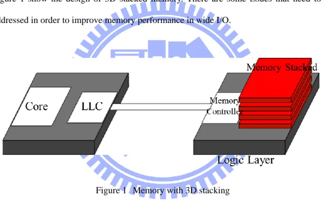
Figure 1 show the design of 3D stacked memory. There are some issues that need to be
addressed in order to improve memory performance in wide I/O.
Figure 1 Memory with 3D stacking
First, balance resource’s utilization by analyzing memory address mapping. Address
mapping affects the banks or ranks usage. It is hard to decide optimized mapping method
for different memory systems because diverse memory hardware constrains and distinct
properties. This work explores wide I/O property with different mapping method by traces
analysis.
3
difficult for prefetcher to get memory state information traditionally because it is designed
close to CPU. With 3D SoC integration, memory controllers can combine more complex
logic design. This thesis proposes adaptive prefetching technique by analyzing memory
block intensively and the possibility of continuous adjacent addresses. In order to reduce
useless prefetch requests, this work further use a set of counters to observe the command
queue state and improve memory rank level parallelism.
Third, open-page row buffer policy is widely used because most programs have spatial
locality when access memory. DRAM controller will issue precharge command to close row
buffers until other command use other rows in the same bank. It may waste power if the row
buffer is not used more efficiently. Moreover, TSV data bus is shared by each rank and
transfers data with burst length mode. The following data commands have to wait for the
transmission complete. This thesis try to pre-issue precharge command when TSV bus is
busy and overlapping the latency.
Finally, discuss the extra hardware cost in our experiment.
1.2 Contribution
1 Provide an ESL platform that can model Wide I/O interface. It can help to evaluate 3D
IC integration development in the early-stage.
2 Using pthread to speed up simulation time.
3 Analyze the address mapping method and property of wide I/O interface.
4 Provide two mechanism: Adaptive prefetching techniques and latency overlapping
4
1.3 Report Organization
The remainder of this thesis’ structure is as follow. Section II introduces the background of DRAM and the policies to improve system performance like prefetching or
predict precharge. Section III describes the framework of our 3D DRAM simulator. Section
IV describes the scheduler and policy to hide latency policy in order to improve the DRAM
access latency. Section V introduces our experiment environment. The result and cost are
also taken into consideration. Finally this thesis compares our method with others and
5
II. Background and Related Work
TSV technology is the trend of future design. This chapter will briefly describe some
basic concepts of DRAM property and 3D wide I/O interface backgrounds. Next, this work
introduces previous works that utilize prefetching and scheduling method to improve
DRAM performance. Finally, we will present a table of analysis advantage and drawback
analysis on those control method in 3D IC era.
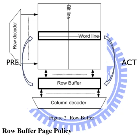
2.1.1 Row Buffer
Row buffer is like a cache of bank arrays. It is a very important component in the
DRAM system because every access will go through this buffer and transfer by amplifier to
enlarge the signal. Figure 2 shows a typical row buffer design. Upon memory access, the
entire row of DRAM bank is amplified by a sense amplifier before loading into row buffer
and in the process, the row data in DRAM is destroyed. This action is called “ACTIVATE”.
After the row buffer is activated, the following row access is related to the row buffer.
Because activate is a destructive access, data must be restored into DRAM before another
row is used. The restore action is called “PRECHARGE”. The maximum number of
activated row buffers is limit per rank. For example, DDR2 and DDR3 use FAW(Four
activated windows), but Wide I/O uses TAW(Two activated windows). Activated command
6
relationship to each operation. “tRCD” is the minimum time interval that can issue memory
access command after the activated action. “tCL” is the minimum timing interval between
memory access command and data put into the data bus. “tRP” is the minimum timing
interval between recharge. “tRCD”, “tRP”, and “tCL” are the most frequently discussed
timing parameter in memory systems.
Figure 2 Row Buffer
2.1.2 Row Buffer Page Policy
While the memory is accessing data, there are three common timing parameters:
precharge, activated, and access column. If the row being accessed is currently opened, it
can directly access data without precharging or activating the row. These three primary row
buffer page policies are open page policy, closed page policy and timing policy.
Open Page Row Buffer Policy
7
for data with spatially locality because the row buffers do not have to be activated
twice in a period. If the access commands are mapped to the same opening row, it can
directly access the DRAM data without other commands. And it will issue
PRECHARGE command until a new command accesses a different row. The open
page policy is widely used in general-purpose computer.
Close Page Row Buffer Policy
Close page policy will close the row buffer as soon as the command access is
completed. It will take advantage of random memory access because it may save
precharge time. If the rate of row buffer hit is low, close page policy may be better than
open page policy.
Timeout Policy
Timeout policy will close the opening row after a time interval. This policy will
provide tradeoff between open and close page policy.
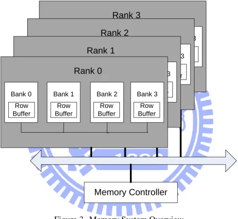
2.1.3 Memory System
Recently the DRAM system has one or more channel controllers design. Each
controller controls a separate portion of the memory system. Because of the command and
data bus are also duplicated, each controller can issue command or access data concurrently
without any dependency.
The basic DRAM system consists of one or more ranks. Each rank has many Banks and
8
system must delay command and pay the rank to rank switch time penalty.
Bank is the basic component of the DRAM system just like a two dimension data array
which is composed by many bit cells. Because each bank in the same rank can work
concurrently, it can hide the latency if multiple banks are activated and accessed data in
parallel. Each bank has a row buffer and the data access must go through the row buffer.
Bank 0 Row Buffer
Bank 1 Bank 2 Bank 3 Row Buffer Row Buffer Row Buffer Rank 3 Bank 0 Row Buffer
Bank 1 Bank 2 Bank 3 Row Buffer Row Buffer Row Buffer Rank 2 Bank 0 Row Buffer
Bank 1 Bank 2 Bank 3 Row Buffer Row Buffer Row Buffer Rank 1 Bank 0 Row Buffer
Bank 1 Bank 2 Bank 3 Row Buffer Row Buffer Row Buffer Rank 0 Memory Controller
Figure 3 Memory System Overview
2.1.4 TSV Technology
TSV is abbreviated from Through-Silicon-Via. The new technology lay chips stack by
stack 3 dimensionally. The delay of TSV is also shorter than tradition horizontal bus.
Memory can be stacked as a cube then add a new dimension call layer. The delay is directly
9
Wide I/O is based on the TSV technology to control data transfer of the stacked
memory. The feature of this device is it can stack up to four layers of memory. There are
four channel controllers in the Wide I/O interface, and each controller controls section of
the memory stack independently. The data bus is 128 bits wide. The total memory size can
be up to in 32 Gb in density. The voltage is only 1.2V and the frequency is 200MHz. Each
layer is an independent system, so the timing constraint is different from transition design.
For example, DRAM system can issue access commands to different rank in succession in a
3D memory system, but traditionally the timing delay constraint is exists which is call Rank
to Rank Switch time. Previous researches [4][5][6] analysis of TSV shows that 3D
integration technology will impact not only memory stacks, CPU caches and cores may also
need to be re-designed. Wide I/O 128 bits Rank_2 Rank_1 Rank_0 Rank_3 Channel_0 Channel_1 Channel_2 Channel_3 Channel Controller Channel Controller Figure 4 TSV Technology
10
2.2 Memory Controller Scheduling
Scheduling policy plays an important role in the Memory system. Because of the
destructive access control in DRAM, the access ordering will impact numbers of precharge
and activate new row into row buffer. Unsuitable access ordering will cause power
consumption and longer access latency. There are many researches about reorder the
command requests to improve the system performance. Different polices optimizes the
scheduler to adapt to a particular property. A good scheduling will improve the DRAM
bandwidth and delay. In this section, this thesis will introduce some state-of-the-art
scheduling policy about DRAM.
2.2.1 FR-FCFS Schedule
Because DRAM access pays less latency penalty when accessing already opened rows,
read latency can be significantly reduce with more page hits. Rixner proposed a scheduling
policy which is called “First Ready-First Come First Serve”[7] and it is the common policy
in today’s memory system. This scheduler will reduce latency as the following timing
diagram. FR-FCFS issues commands to already opened row buffer over other requests. It is
just like a greedy algorithm scheduling policy for improving row buffer hit ratio. If there are
no opening requests that can be issued now, the scheduler will prioritizes and issue oldest
11
Figure 5 FR-FCFS Command Scheduling
2.2.2 Fairness Scheduling
Because FR-FCFS scheduling policy is a greedy algorithm, it may cause starvation
when some requests are continuously served in the period. A memory intensive program
will send a lot of memory requests to DRAM and be issued quickly because the possibility
of those rows being opened is higher than other request. Other requests will delay for a long
time and programs will be stall because the data is not return from memory. Some
researches take requests waiting time into consideration and adjust the controller’s request
priority periodically. For example, the scheduler can give basic priority number for requests
and increase it after a time interval. This action gives higher priority to the older requests,
thus the read request delay times are more balance. The priority aging[8] concept will
reduce the unfairness situation for solving starvation and it is important since it affects the
CPU waiting time. There is a tradeoff between performance and fairness because it breaks
the continuous row buffer access times for fairness scheduling. Memory timing constraints
should also be taken into considers. Virtual writing queue[9] reduces memory read to write
delay penalty. By handling write command separate from read, this mechanism helps to
12
Thread status can also issue to the memory scheduling, because of shared cache
replacement and data bus, many resource may cause contentions. ATLAS[10] is a memory
scheduling algorithm that improves system throughput by prioritizing threads that have
smaller attained memory service. Those threads may more likely be memory non-intensive
and improve performance significantly by serving those threads’ request soon. PAR-BS[11]
focuses on thread fairness and prevent short term and long term starvation by taking
registers info per request and thread ranking. Although there are many method to improve
memory performance, most of them have to bypass some information from CPU to memory
controller and the design must also be constrained.
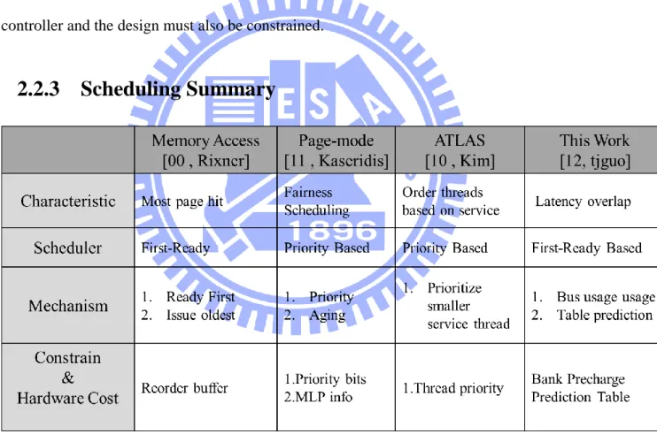
2.2.3 Scheduling Summary
Table 1 Comparison of Scheduling
Many scheduling are based on FR-FCFS policy to improve performance, and pass
information from CPU by adding extra cache tag. This method will increase bus
13
issue precharge command early and overlap the bus transmission time.
2.3 Prefetch Policy
Prefetching mechanism can predict the next address and fetch data beforehand. Stream
prefetcher can keep track of multiple access streams. “Prefetch Distance” and “Prefetch
Degree” determine the aggressiveness of the prefetcher. Aggressive prefetching mechanism
can improves performance, but miss fetch in some benchmark decreases system
performance.
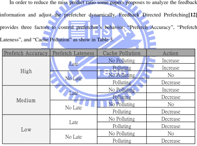
In order to reduce the miss predict ratio some papers proposes to analyze the feedback
information and adjust the prefetcher dynamically. Feedback Directed Prefetching[12]
provides three factors to control prefetcher’s behavior: “Prefetch Accuracy”, “Prefetch
Lateness”, and “Cache Pollution” as show in Table 3.
Prefetch Accuracy Prefetch Lateness Cache Pollution Action
No Polluting Increase Polluting Increase No Polluting No Polluting Decrease No Polluting Increase Polluting Decrease No Polluting No Polluting Decrease No Polluting Decrease Polluting Decrease No Polluting No Polluting Decrease Medium Low Late No Late Late No Late Late No Late High
Table 2 FDP Control Table
As soon as the prefetching data returns, it will update the information and determine
whether to use prefetcher or not. These prefetchers are often incorporated in cores and
14
of the prefetch requests, the Last Level Cache has to add the entry to identify the demand
requests and prefetching requests. It is an overhead in overall architecture and does not fit
the DRAM property. Coordinated control [13] solves the problem about inter-core prefetch
requests conflict in cache. Prefetcher causes inter-core interference and may diminish
prefetching’s potential performance. In order to reduce conflict, it adds an extra center
controller to manage which prefetch requests can be sent into memory system. Lee et al.[14]
combines the prefetcher and memory architecture to improve bank level parallelism. Bank
is the basic component of the memory system, each bank can work independently. The
concept of bank level parallelism is to overlap delay by access bank concurrently.
BLP-Aware Prefetch Issue will keep track of which bank the prefetching requests will be
issued to and issue them out of order to improve the bank utilization. Furthermore,
BLP-Preserving Multi-core Request Issue Policy also considers the prefetching requests
from multi-core. It controls the order of prefetching requests and issues those from the same
core first. This mechanism minimizes the destructive interference in the BLP of each
program.
The general priority schedulers that deals with prefetch requests can be put into two
categories, one type of prefetching request schedulers[15–17] gives less priority to
prefetching requests than normal request. Since the prefetcher is assigned lower priority, the
normal request will be issued faster than the predicted prefetching requests. It will drop the
prefetching request if the prefetching requests waiting time is too long, as it is more likely
te be a useless demand. The other policy[18] treats prefetching requests as a demand request.
So it will schedule equally and fairly performance if the prefetcher prediction hit rate is
15
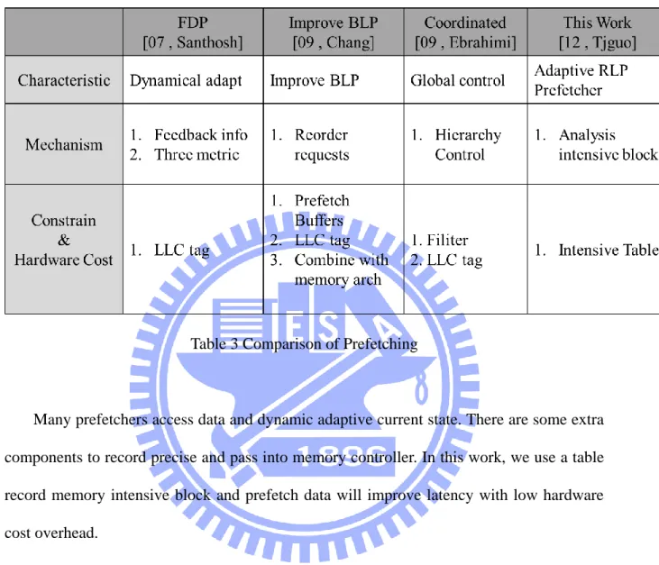
2.3.1 Comparison of Prefetch Mechanism
Table 3 Comparison of Prefetching
Many prefetchers access data and dynamic adaptive current state. There are some extra
components to record precise and pass into memory controller. In this work, we use a table
record memory intensive block and prefetch data will improve latency with low hardware
16
III. 3DRAMSim Framework
3.1 Overview
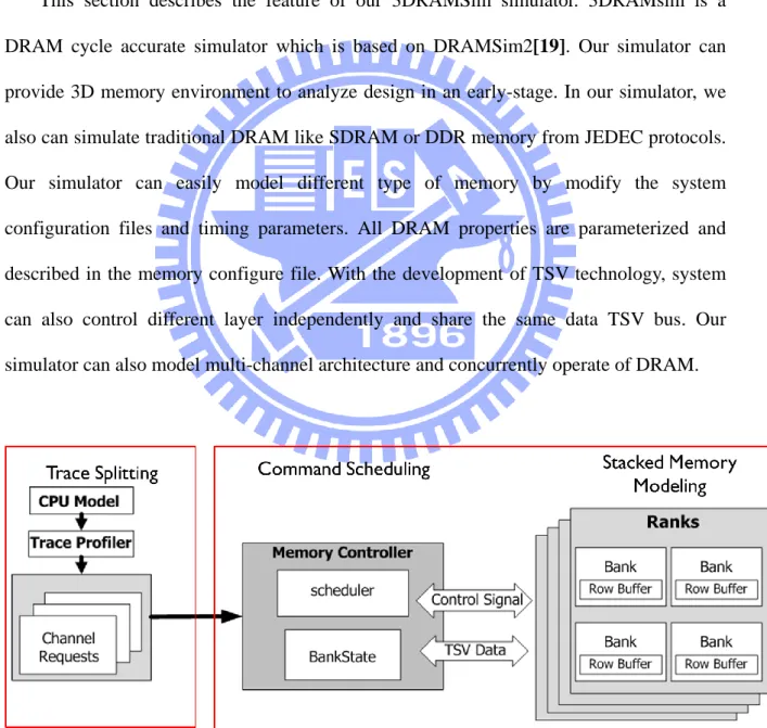
This section describes the feature of our 3DRAMSim simulator. 3DRAMsim is a
DRAM cycle accurate simulator which is based on DRAMSim2[19]. Our simulator can
provide 3D memory environment to analyze design in an early-stage. In our simulator, we
also can simulate traditional DRAM like SDRAM or DDR memory from JEDEC protocols.
Our simulator can easily model different type of memory by modify the system
configuration files and timing parameters. All DRAM properties are parameterized and
described in the memory configure file. With the development of TSV technology, system
can also control different layer independently and share the same data TSV bus. Our
simulator can also model multi-channel architecture and concurrently operate of DRAM.
17
Figure 6 illustrates the 3DRAMSim flow diagram. The proposed simulator includes
three parts: trace splitter, memory controller, and memory storage. The trace splitting stage
includes overall system timing control, and address mapping analysis tool. In order to
simulate the multi-channel environment, trace must be pre-process, split into sub-traces and
issued by each channel controller. Trace splitting has to know the address mapping method
and separate requests mapping into their sub-trace. After the trace splitter, each controller
increases their own timing domain count. If this counter is less than the trace’s timestamp,
the trace will issue until the counter equal to the timestamp and another request will not be
issued in the same channel. After all trace are finish, system will show those information
and physical execute time to help us evaluate our design.
3.2 Parameter Design
Many specifics described as parameters, can improve program flexibility and usability.
It can simulate other memory architecture by modifying some critical property with low
overhead. There are two classic configurations for our simulator.
First, memory configuration file will provide the timing and current parameter. It also
gives the architecture structure information for DRAM like number of banks and ranks.
Second, system configuration file provides the policies for our target DRAM. These
policies include row buffer policy, memory address mapping, and scheduling method. With
many policies, we have to modularize respective functions to make the program more
readable and easy to expand.
Finally, we use indirect pointer to link the function section in the initial time to save the
18
this pointer to call specific function directly. It can easily switch to other policies without
recompilation of the program, making it more efficiency.
3.3 Channel Controller
BankState is a table that describe the current bank state including current row buffer
state, current command issued, and requests action corresponding to reasonable cycle time
to fit the timing constrain. This state table will determine when the command can be issued
or not in this cycle and update the table state whenever a command is committed.
Channel controller is the main control of the memory system and operates disjointed
portions of memory stack independently. Command queues store those memory requests
scheduled by the scheduler in the buffers. Commands sequence will be reordered and issued
out of order to improve the memory performance. In our 3DRAMsim simulator, this work
provides the well-know FR-FCFS scheduling policy.
Each controller access a portion of the memory stack. They do not cause interference
and the clocks are maintained by its own domain. The timing clock is store in the controller
object and increases every time controller update called by the upper system. As soon as the
timer increases, next cycle will come and schedulers compare the bank state timing
constraint with the current clock to schedule those commands.
3.3.1 TSV Modeling
All ranks are shared by the same TSV bus in region of the same channel controller. The
19
TSV is 300 in wide I/O interface for each controller. Controller can continuously send a
command to different ranks every cycle if the command conforms to the timing constrain.
Because wide I/O is burst oriented, all the data accesses are uses burst mode to transfer.
The data bus must be locked a period by data burst transfer with many cycles. In wide I/O
interface, the burst length is either two or four cycles. Also, the stacked memory property
only restricts each timing constraint in the current rank. In other word, the data commands
may be sent continuously. The data bus competed by controllers, so it must have an arbiter
to determine which one can use TSV data bus in this period and when to release the
resource. There is a counter in our wide I/O bus model. It will add burst length to reflect
the bus transfer when the arbiter decides which controller has the next period. Memory
controller will call the lock function to prevent different ranks using the TSV bus when
transaction is not complete. After TSV data bus is locked, the counter will count down to
zero and then unlock the data bus. If the bus is free, the controller will select the earliest
command for scheduling and lock the data bus. It will simulate command continuously and
access data sequentially to transfer. Our TSV bus modeling can more accurately describe
data bus utilization. Simulator can also reflect the bandwidth by calculating the locking
cycle. It is an important metric for memory intensive programs.
In order to save power, it can switch to low power mode if the command queue is
empty and the state is idle for a rank. If there are other commands injected into the
command queue, the rank will switch to normal mode after in a period. It can calculate the
20
3.4 Accelerating Simulation
In recent development, DRAM has more and more ranks and controllers to improve
access latency. With the simulation components increasing, simulation time also become
much longer because each object has to update its state or transfer data every cycle in the
simulator. Some of them are unnecessary updates only check and increase cycle when the
command queue is empty. There are many potential opportunities to speed up the DRAM
simulator. For example, the previously mentioned indirect pointer saves unnecessary
comparison time when program executes. Also, it can find and improve program parallelism
issues to speed up simulation time. Our speedup mechanism in the 3DRAMsim focuses on
channel controllers because the control, data, and clock signals are critical to independent
control. It means different channel controllers can be executed on their own and the
executions are likely to be parallelized. Furthermore, the result of the speedup version must
be the same as original version to prove the correctness. In order to speed up the channel
controllers, this work has to modify the program execute about the channel update function.
The original version updates channel use loop and update sequentially whenever system
cycle increase and the ordering will not be affected because the controllers are independent.
If the system only has one trace for simulator, it is hard to reflect concurrent execution
for a multi-channel architecture. The trace splitter is described in the previous section. After
the memory system is created, it also creates many threads for each channel controller in
our simulator. Figure 7 show the concept of the thread creation for each channel. In our
multi-thread version, each thread updates their own ranks partially without dependency. The
simulation cycle is the maximum cycles in all the sub-trace returned from the trace splitter.
Because of threads’ difference in speed, it has to wait for all controller threads to finish its
21
not. The program will insert a barrier to wait for the slower job and print all the information
after all controllers simulate completed. The result in both versions must match to verify the
speedup version’s correctness.
CPU Model
Trace Porcessor Channel Controller Ranks Channel Controller Ranks Channel Controller Ranks Channel Controller RanksFigure 7 Pthread Accelerating Method
Figure 8 show our simulator speeds up 3.1 times compare to sequential version in
average. Considering threads diversity, some threads have to wait for the slowest one, the
degree of speedup is always nearly the number of threads if host machine has enough cores
and can support threads to execute independently. The maximum speedup will be
proportional to the number of channels and the upper bound is four times in wide I/O
22
Figure 8 Simulation Speedup Times
3.5 Profile Model
With the TSV technology coming, there are some differences from traditional DRAM
memory system. Controllers can issue different command to every rank by interleaving. The
rank can issue commands only when sharing the same data bus. The timing constraint in
different ranks only have to consider their layer inside. The property of the parallelism
factor will also be different because the ranks behavior also changes. For example, the rank
to rank switch time will impact the rank level parallelism and the activated row buffer
constraint will impact bank level parallelism. There are more complex factors for 3D IC
development, and the best addressing mapping policy will become harder to find. Our
simulator provides some simple methods that can find a better mapping method to fit your
demand. Better mapping methods can be found by two steps. After mapping analysis, the
simulator will find the trend of different mappings for the current architecture.
First step of evaluation is focused on the rank and channel utilization in the memory
23
channels mapping are unbalanced, it will cause some resource to idle, causing violent
competition in some rank. This step will eliminate the most of the impossible mapping
methods, but some case is hard to find because the number of commands will continued to
increase in disperse ranks for a long time.
Second, memory level analysis is important to mapping performance. It will run
3DRAMsim with trace by without timestamp. This step will show parallelism because the
command dependency will be roughly taken into consideration. The simulation time is
faster than the complete simulation because it does not have to wait for the trace interval for
command issues. This work chooses those potential methods as candidates and analyze
artificially. The traditional mapping methods consider the bank level parallelism and
column access locality in the simple memory system.
The results show mapping channel’s bits to lowest bits is better because when mapped
to upper bits, the bits are more unbalanced and have less channel level parallelism, since
having independent channel controllers achieves the maximum parallelism. Moreover, the
row bits are mapped to higher bits because this way there is no parallelism issue between
each row. If the row bits are mapped to the lower bits, it may more likely use a different row
24
IV. Control Mechanism
4.1 Address Mapping Analysis
Semi-automatic method can eliminate those low performance combination mapping. It
shows the row bits mapping to high and channel bits mapping to low get better performance
for wide I/O interface. This thesis analyzes the other parallelism issue to fit the 3D
architecture by run simulation completely. The results of different mapping show in Figure
9 as follow and find the best mapping method. The value is normalized to the first mapping
method.
The x-axis is mapping sequence’s permutation combination of rank, bank, and column.
The first and second methods are mapping column bits to lowest. The third and fourth are
rank lowest, and the others are bank-orient. This work finds the rank will get the best
performance if mapping to the lowest bits. Because of each layer can work independently
with low overhead rank to rank switch penalty and only shared the same TSV bus to
25
Figure 9 Different Address Mapping Method
(R: Rank / B: Bank / C: Column)
Bank level parallelism will not improve well in our simulation result. It may cause by
opening windows constrain in rank constrain in wide I/O interface. The maximum number
of row buffer be activated is two. It has to close some row buffer to open another, and the
delay penalty will decrease the system performance. This work will select the following
mapping sequence: “Row:Column:Bank:Rank:Channel” to evaluate our following
experiment.
4.2 Adaptive Prefetching Engine
OS manage the all resources allocation in general computer architecture. The memory
26
address and then convert to physical address by MMU. Memory controller must access data
with physical address. Page is based on the size of block and must be the same in virtual
and physical memory. Page size is normally set range size from 2 to 8KB. The same
application will be allocated to continuous virtual address but it will be mapping to discrete
physical block. Because programs have spatial locality, the nearly address may appear soon.
This behavior is the same in physical page block. This thesis analyzes the behavior in
physical block and prefetch data to improve performance. Our mechanism is much different
from other that this work not focus on core level prediction but physical behavior to find
memory intensive block.
TSV technology can stack different fabrication process and design more flexible. With
three-dimension integration memory layers stacked on top of logic memory control layer.
Memory and CPU can design independently and optimal by themselves. The control can be
aimed at controller and dynamic adaptive with DRAM state. Prefetching is general way to
improve DRAM performance and combine with core. Because the Prefetcher is separated to
DRAM system, it is hard to get the current memory state and only determine by return
requests’ information. In order to get more power information, the LLC must add column
and bypass to CPU. This mechanism will increase cache size and power consumption.
Prefetcher doesn’t always improve system performance due to some reasons. First, miss-predict request will waste the memory bandwidth. Because one channel is shared by
many banks, the useless prefetching request will block the TSV bus and delay demand
requests. The extra fetch data will affect the system behavior for example access other row
buffer. For some critical example, the prefetching mechanism will degrade memory system
performance a lot. Second, extra prefetch request will replace original data in cache. The
27
our prefetching will combine with controller and depend on memory rank state. This work
also adds an extra cache for our prefetch requests in the 3D memory logic layer.
4.2.1 Prefetching Reference Table
There is address spatial locality property when memory access. Although virtual address
translates to physical with discrete mapping, the same virtual memory block will be
mapping to the same physical block. With the memory intensive access program, the
continuous address would likely access soon with regular address interval. In this case,
memory access pattern will probability to predict the next memory address. On the other
hand, Memory non-intensive programs will hard to predict with memory analysis.
In order to distinguish memory intensive blocks, there is a cache table to record the
memory block utilization. The address is based on the block numbers to record the access
status. The access in the block are using an accuracy counter to reflect the continuously
access in a restrict region. This thesis selects partial bits in physical address as our tag and
index as Figure 10 illustrate. For example, if block size is 4KB with 8GB memory system,
the address has to shift right it mean there are total 2M blocks which size is in
our system. In order to reduce extra cost for record all 2M entry block, this work use a
28
Figure 10 Prefetching Table
4.2.2 Adaptive-Prefetching Control
In order to reduce useless prefetch requests, the control will not only reference the
prefetching table but collocation with rank state restriction. Our prefetching control flow is
show in Figure 11.
First, this work adaptives the prefetch degree depend on the accuracy in reference.
There is a threshold to restrict the Prefetcher. If the counter higher than threshold, the
different prefetching degree is depend on the accuracy counter. Second, many researches
show the prefetch requests will more likely useless if the request is delay for a long time. In
our design, the prefetch request will insert depend on the command queue entry size. If the
command buffer is already has many requests, prefetch request will be delayed because it
has to process previous request no matter in FCFS property scheduling or demand first
priority based scheduling. In other word, prefetch requests will access data and waiting for a
long time. The advantage of prefetching mechanism will decrease. To prevent this case, our
29
prefetching request or not.
Prefetch Table Hit T F Update tag & Counter=0 Accuracy Counter > Threshold F T No Prefetch Request Insert Prefetch Request Last_addr -addr < range Accuracy counter--T F Accuracy
counter--Figure 11 Prefetching Flowchart
4.3 Hide Latency Scheduling
Memory Stacked will improve the system performance and change the memory
property when TSV technology matures. With 3D architecture, there is some opportunity to
optimize the overall system. For example, controller can continuously issue command to
each rank because zero rank to rank switch delay. The rank switch overhead will become
small than before. Continue access different layers data in 3D memory use the same TSV
bus. Memory controllers have to determine which rank can transfer data. Data will delay
30
controllers lock the TSV bus, it will release many cycles decide by the data burst length. In
other word, next data command will be delay by previous request because the TSV bus
resource is not release yet. In those waiting cycle, other ranks will have opportunity to issue
command and the delay will be overlapped.
FR-FCFS is the most popular scheduling for the DRAM memory system now. It
schedules ready request first and promote the row buffer hit ratio. Most research is based on
this algorithm to improve in case study. The scheduling is not optimized for 3D stacked
memory when the rank to rank switch penalty disappears.
Figure 12 Timing Diagram for Hide Latency Scheduling
Figure 12(a) show the case when continue issue data accessing commands to different
rank. In this case, R0 issue first and R1 after it immediately. The TSV data bus will become
bottleneck and R1 data has to wait for R0 transfer complete. Figure 12(b) is optimized for
this situation. As soon as data access command will be served, there is an opportunity to
issue commands to those not use data bus because the next data will wait for controller
31
In order to improve the performance, Memory controllers can previous precharge the
row buffer when the bus is busy. This work uses a counter which is call BLCD(Bus Length
Counter Down) to express data utilization and exist in each bank. Whenever controllers
server a request, the BLCD will increase number of burst length. BLCD counter will count
down every cycle until zero.
Our algorithm will get those requests which not use data bus higher priority when the
periods of data transferring delay. To reduce miss predict close page probability, there is a
table to record the last row access status recently. The precharge table provides previous
row access information. When a new row is activated, controller will search precharge table
and load value into row predict counter.
“Row prediction counter” store last row access times. The other counter is called access counter, it will use 4 bit saturating counter and express current row access times. If row
access counter is larger than row predict counter, the row will probability close soon.
Predict close row buffer will bring some advantage. First, command issue when TSV bus is
busy and hide precharge latency as show in Figure 12. Second, predict close row buffer will
save power because the activated row buffers will cause more power consumption than
close buffer. Open page policy will hold data until the precharge command issue. In other
word, more power waste because recharge comes too late.
32
Looking for the BLCD to determine whether issue precharge or not. If the BLCD is not
equal to zero, the row predict counter will compare to access counter. When the row predict
counter is bigger the precharge will issue to rank, or it will follow original schedule to issue
command. The control flow is described in Figure 14.
F
T
Next Cycle
&
BLCD
--BLCD += x
Request
Ready
Prioritize
Oldest
T
F
PRECHARGE
Row Buffer
T
F
FR-FCFS
Scheduling
Predict PRE
BLCD == 0
33
V. Experimental Results
5.1 Environment Setup
5.1.1 System Configuration
Table 4 System Configuration
This work uses GEM5 which is a full system simulator to get the memory traces. Our
34
target simulator environment. The memory trace information include timestamp and
physical memory address are generated by running benchmark on GEM5. This thesis
evaluate the DRAM system with parsec[20] and spec2006[21] benchmark which supplies
parallel program and memory intensive workload. The detail benchmark is show detail in
table 6. Application blackscholes in_64K bodytrack sequenceB_4 4 4 4000 5 0 8 facesim timing freqmine kosarak_990k.dat 790 x264 eledream_640x360_128.y4m 401.bzip2 input.program 5 429.mcf inp.in 444.namd --iterations 1 450.soplex m10000 458.sjeng 464.h264ref foreman_encoder_baseline.cfg 470.lbm reference.dat 473.astar lake.cfg 483.xalancbmk xalanc.xsl spec2006
parsec 8 channel / Large
Parameter
test
Table 5 Overview of Benchmark
The memory configuration is described our memory system timgin constrain parameter.
35
Name
Description
Value
tCK
Clock
5ns
RL
CAS latency
15ns
tRCD
Row to column Delay
18ns
tRP
Row recharge delay
18ns
tRAS
Row active time
42ns
tRFC
Refresh time
210ns
tTAW
Two bank active widwow
50ns
tREFI
Refresh time interval
3.9 us
tWTR
Write to read delay
15ns
tRRD
Row to row active delat
10ns
tXP
Power down
10ns
BL
Burst length
4
Table 6 Memory Configuration
5.1.2 Power Model
Wide I/O interface is a new technology and not release physical specific with product
yet. This work selects LPDDR2 as reference target because its property is close to Wide I/O.
Our power parameter reference Micron LPDDR2 to analysis new design in trend. The
power formula is voltage multiple current. There are two voltages support in LPDDR2:
VDD1 is set to 1.8V and VDD2 is set to 1.2V. The current multiple correspond voltage and
accumulate when following status occur. If controller issue some commands the action
power will be accumulated. Otherwise, background calculates DRAM idle power and
different from DRAM power mode and row buffer status. Table 8 shows LPDDR2 power
36
Table 7 LPDDR2 Power Parameter
5.2 Precharge Prediction Analysis
Because some compoments of our control mechanism is an extra overhead, this thesis
takes not only performance but also hardware cost overhead into consider. The extra
precharge mechanism in our design using a precharge prediction table to record the row
37
Figure 15 Precharge Prediction Table Size
The x-axis is the number of table entries and the y-axis is improvement percentage by
original. The average line is increasing rapidly before the table entries is 16. It grows slowly
and saturation when the number is greater than 16 because the buffer will not change row
frequently in a period. It may be caused by RLP-oriented address mapping and FR-FCFS
38
Figure 16 Latency Improvement by different Scheduling
39
Figure 16 show the latency in our Latency overlapping scheduling by precharge
prediction and compare to the MLP scheduling. MLP scheduling separate read/write in
different command queues and issue write command only when the number of write exceed
threshold. Our method is less than MLP scheduling by improvement latency because MLP
save not only read to write timing delay but prioritizes the read command. Figure 17 show
our method can help to save power because pre-close row buffer can use lower current and
more power efficiency. Because our scheduling is control those precharge command in bus
busy slot, it’s independently with MLP scheduling. The result shows our method can
combine MLP scheduling without conflict.
5.3 Adaptive-Prefetch Analysis
40
Figure 18 shows our analysis about prefetch cache size. The x-axis is the number of
table entries and the y-axis is memory improvement by original version. Because each entry
size is up to 64B to store full cache block data. The prefetch cache size will increase rapidly
if the cache extend. In our analysis, when table is larger than 128 entries, the performance
will improve slowly but double the cache size because the prefetch requests not
replacement so frequently and the size is enough. This work selects 128 as prefetch cache
entries.
Figure 19 Improvement Relative to No Threshold Prefetching
In order to reduce useless prefetch request and improve rank level parallelism, this
work proposes constrain the number of prefetch requests when the command buffer exist
requests more than a threshold. This method not only helps to reduce useless prefetch
requests but also rank balance. Figure 19 indicates threshold is set to quarter of command
41
Figure 20 Prefetch Cache Hit Rate
Figure 20 show the hit ratio is nearly 50% accuracy in our adaptive-prefetching
technique cache.
42
Figure 22 DRAM Power Overhead by Adaptive-Prefetching Technology
Figure 21 show our adaptive-prefetching mechanism performance improvement of
DRAM latency. It will improve nearly 11.7% in average. Our control will limit prefetch
requests so the performance is also limited. Figure 11 show the extra energy overhead.
Although prefetch mechanism can reduce latency, useless data will cause extra power
43
5.4 Hardware Cost
Table 8 Precharge Predict Overhead
Table 8 show the hardware overhead of latency overlapping scheduling implement.
Because the precharge predition table is exist in each bank. The table size has to multiple to
number of bank.
Table 9 Adaptive-Prefetch Overhead
Table 9 show the cost for Prefetching mechanism and cache. Because the prefetcher
and cache exist in each channel controller. The table size has to multiple to number of
44
VI. Conclusion
This thesis provides an ESL platform with TSV architecture that can support wide I/O
interface. Our simulator is modularize with configurable design parameters so it’s ease to
model different architecture. This work also speedup the simulation time by using pthread
acceleration method for each channel. The speedup is approximate 3.1 times with four
channel controller design relative to sequential version.
With analysis of different memory mapping methods in wide I/O, results show that rank
level parallelsim is good for 3D design because the rank to rank switch penalty decreases
and the maximum number of activated windows is constrained.
Finally, this work proposes two mechanisms to improve system performance. Adaptive
prefetching techniques analyzes memory intensiveness and access locality to prefetch data
and considers the number of rank command to improve latency nearly by 13% with 3.5%
power overhead. Latency overlapping schedules ahead of precharge command by
overlapping TSV data transfer delay. Latency overlapping scheduling helps to reduce 0.6%
latency and save 4% power consumption by pre closing row buffers.
The hardware cost is an extra overhead in design. This work tradeoff overhead to get
45
References
[1] C. Weis, N. Wehn, L. Igor, and L. Benini, “Design space exploration for
3D-stacked DRAMs,” in Design, Automation Test in Europe Conference Exhibition (DATE),
2011, pp. 1 –6 (2011).
[2] C.-H. Lin, W.-T. Hsieh, H.-C. Hsieh, C.-N. Liu, and J.-C. Yeh, “System-level
design exploration for 3-D stacked memory architectures,” in 2011 Proceedings of the 9th
International Conference on Hardware/Software Codesign and System Synthesis (CODES+ISSS), p. 389 (2011).
[3] J.-S. Kim, C. S. Oh, H. Lee, D. Lee, H. R. Hwang, S. Hwang, B. Na, J. Moon,
J.-G. Kim, et al., “A 1.2 V 12.8 GB/s 2 Gb Mobile Wide-I/O DRAM With 4 * 128 I/Os
Using TSV Based Stacking,” IEEE Journal of Solid-State Circuits 47, 107 –116 (2012).
[4] G. H. Loh, “3D-Stacked Memory Architectures for Multi-core Processors,”
SIGARCH Comput. Archit. News 36, 453–464 (2008).
[5] K.-M. Choi, “An industrial perspective of 3D IC integration technology from the
viewpoint of design technology,” in Design Automation Conference (ASP-DAC), 2010 15th
Asia and South Pacific, pp. 544 –547 (2010).
[6] I. Loi and L. Benini, “An efficient distributed memory interface for many-core
platform with 3D stacked DRAM,” in Proceedings of the Conference on Design,
Automation and Test in Europe, pp. 99–104, European Design and Automation Association,
3001 Leuven, Belgium, Belgium (2010).
46
access scheduling,” 2000, New York, NY, USA, 128–138, ACM.
[8] D. Kaseridis, J. Stuecheli, and L. K. John, “Minimalist open-page: a DRAM
page-mode scheduling policy for the many-core era,” 2011, New York, NY, USA, 24–35,
ACM.
[9] J. Stuecheli, D. Kaseridis, D. Daly, H. C. Hunter, and L. K. John, “The virtual
write queue: coordinating DRAM and last-level cache policies,” 2010, New York, NY, USA,
72–82, ACM.
[10] Y. Kim, D. Han, O. Mutlu, and M. Harchol-Balter, “ATLAS: A scalable and
high-performance scheduling algorithm for multiple memory controllers,” January 2010,
1 –12.
[11] O. Mutlu and T. Moscibroda, “Parallelism-Aware Batch Scheduling: Enhancing
both Performance and Fairness of Shared DRAM Systems,” 2008, Washington, DC, USA, 63–74, IEEE Computer Society.
[12] S. Srinath, O. Mutlu, H. Kim, and Y. N. Patt, “Feedback Directed Prefetching:
Improving the Performance and Bandwidth-Efficiency of Hardware Prefetchers,” February
2007, 63 –74.
[13] E. Ebrahimi, O. Mutlu, C. J. Lee, and Y. N. Patt, “Coordinated control of multiple
prefetchers in multi-core systems,” December 2009, 316 –326.
[14] C. J. Lee, V. Narasiman, O. Mutlu, and Y. N. Patt, “Improving memory bank-level
parallelism in the presence of prefetching,” 2009, New York, NY, USA, 327–336, ACM.
[15] D. Joseph and D. Grunwald, “Prefetching using Markov predictors,” in
Proceedings of the 24th annual international symposium on Computer architecture, pp.
252–263, ACM, New York, NY, USA (1997).
47
challenges,” in 11th International Symposium on High-Performance Computer Architecture,
2005. HPCA-11, pp. 248 – 252 (2005).
[17] I. Hur and C. Lin, “Adaptive History-Based Memory Schedulers,” in Proceedings
of the 37th annual IEEE/ACM International Symposium on Microarchitecture, pp. 343–354,
IEEE Computer Society, Washington, DC, USA (2004).
[18] C. Zhang and S. A. McKee, “Hardware-only stream prefetching and dynamic
access ordering,” in Proceedings of the 14th international conference on Supercomputing,
pp. 167–175, ACM, New York, NY, USA (2000).
[19] P. Rosenfeld, E. Cooper-Balis, and B. Jacob, “DRAMSim2: A Cycle Accurate
Memory System Simulator,” Computer Architecture Letters 10, 16 –19 (2011).
[20] C. Bienia, S. Kumar, J. P. Singh, and K. Li, “The PARSEC benchmark suite:
characterization and architectural implications,” in Proceedings of the 17th international
conference on Parallel architectures and compilation techniques, pp. 72–81, ACM, New
York, NY, USA (2008).
[21] J. L. Henning, “SPEC CPU2006 benchmark descriptions,” SIGARCH Comput.