行政院國家科學委員會專題研究計畫 成果報告
金屬微結構之製程及其應用之研究
計畫類別: 個別型計畫
計畫編號: NSC93-2212-E-009-019-
執行期間: 93 年 08 月 01 日至 94 年 07 月 31 日
執行單位: 國立交通大學機械工程學系(所)
計畫主持人: 徐文祥
報告類型: 精簡報告
報告附件: 出席國際會議研究心得報告及發表論文
處理方式: 本計畫可公開查詢
中 華 民 國 95 年 1 月 29 日
行政院國家科學委員會補助專題研究計畫
行政院國家科學委員會補助專題研究計畫
行政院國家科學委員會補助專題研究計畫
行政院國家科學委員會補助專題研究計畫
■
■ 成 果 報 告
■
■
成 果 報 告
成 果 報 告
成 果 報 告
□
□
□
□期中進度報告
期中進度報告
期中進度報告
期中進度報告
金屬微結構之製程及其應用之研究
計畫類別:■ 個別型計畫 □ 整合型計畫
計畫編號:NSC 93-2212-E -009 -019 -
執行期間: 93 年 8 月 1 日至 94 年 7 月 31 日
計畫主持人:徐文祥
共同主持人:
計畫參與人員: 鍾君煒 何鍵宏
成果報告類型(依經費核定清單規定繳交):■精簡報告 □完整報告
本成果報告包括以下應繳交之附件:
□赴國外出差或研習心得報告一份
□赴大陸地區出差或研習心得報告一份
■出席國際學術會議心得報告及發表之論文各一份
□國際合作研究計畫國外研究報告書一份
處理方式:除產學合作研究計畫、提升產業技術及人才培育研究計畫、列
管計畫及下列情形者外,得立即公開查詢
□涉及專利或其他智慧財產權,□一年□二年後可公開查詢
執行單位:國立交通大學機械系
中 華 民 國 94 年 7 月 31 日
行政院國家科學委員會專題研究計畫成果報告
金屬微結構之製程及其應用之研究
The Fabrication of Metal Micro Structure
and Its Application
計劃編號 :
NSC 93-2212-E009-019
.執行期間 :
93 年 8 月 1 日至 94 年 7 月 31 日
計劃主持人 : 徐文祥 國立交通大學機械系教授
計畫參與人員:鍾君煒 李毅家 國立交通大學機械所研究生
一
一
一
一、
、
、中文摘要
、
中文摘要
中文摘要
中文摘要
本計畫 本計畫 本計畫 本計畫主要在發展主要在發展主要在發展主要在發展金屬式微加工技術金屬式微加工技術金屬式微加工技術之製作金屬式微加工技術之製作之製作之製作 平台 平台 平台 平台,,,,包含改善固定結構之製作效率包含改善固定結構之製作效率包含改善固定結構之製作效率包含改善固定結構之製作效率、、、發展懸浮、發展懸浮發展懸浮發展懸浮 結 結 結 結構之製作平台及以此構之製作平台及以此構之製作平台及以此平台構之製作平台及以此平台平台平台發展優化致動引擎及發展優化致動引擎及發展優化致動引擎及發展優化致動引擎及 其相關應用 其相關應用 其相關應用 其相關應用。。。就固定金屬結構之製作而言。就固定金屬結構之製作而言就固定金屬結構之製作而言就固定金屬結構之製作而言,,,,以以以嵌以嵌嵌嵌 入法之應用經驗為基礎 入法之應用經驗為基礎 入法之應用經驗為基礎 入法之應用經驗為基礎,,,,建立完善的嵌入法特性建立完善的嵌入法特性建立完善的嵌入法特性建立完善的嵌入法特性 研究資料 研究資料 研究資料 研究資料,,,以提高現有,以提高現有以提高現有金屬式微加以提高現有金屬式微加金屬式微加金屬式微加工技術之製作工技術之製作工技術之製作工技術之製作 效率 效率 效率 效率。。。。就懸浮金屬結構之製作而就懸浮金屬結構之製作而就懸浮金屬結構之製作而就懸浮金屬結構之製作而言言,言言,,,採採採用金屬犧採用金屬犧用金屬犧用金屬犧 牲層產生 牲層產生 牲層產生 牲層產生垂直垂直垂直空間並搭配金屬垂直空間並搭配金屬空間並搭配金屬空間並搭配金屬回填回填的概念回填回填的概念的概念的概念,,,,發展發展發展發展 垂直空間式金屬犧牲層 垂直空間式金屬犧牲層 垂直空間式金屬犧牲層 垂直空間式金屬犧牲層(VSMSL)的懸浮結構製作的懸浮結構製作的懸浮結構製作的懸浮結構製作 平台 平台 平台 平台,,,,此製作平台可提供高效率出平面運動致動此製作平台可提供高效率出平面運動致動此製作平台可提供高效率出平面運動致動此製作平台可提供高效率出平面運動致動 引擎之製作 引擎之製作 引擎之製作 引擎之製作。。。此外。此外此外此外,,,亦將對致動引擎進行優化設,亦將對致動引擎進行優化設亦將對致動引擎進行優化設亦將對致動引擎進行優化設 計 計 計 計,,,以提供高效率之致動能力,以提供高效率之致動能力以提供高效率之致動能力以提供高效率之致動能力,,,,進而以此平台技進而以此平台技進而以此平台技進而以此平台技 術及致動引擎為基礎 術及致動引擎為基礎 術及致動引擎為基礎 術及致動引擎為基礎,,,,發展發展發展發展相關應用元件相關應用元件相關應用元件。相關應用元件。。。穩定穩定穩定穩定 的金屬式微加工平台除了發展元件之應用外 的金屬式微加工平台除了發展元件之應用外 的金屬式微加工平台除了發展元件之應用外 的金屬式微加工平台除了發展元件之應用外,,,未,未未未 來亦深具系統整合發展之潛力 來亦深具系統整合發展之潛力 來亦深具系統整合發展之潛力 來亦深具系統整合發展之潛力。。。 。英文摘要
英文摘要
英文摘要
英文摘要
The primary goal of this project is to develop the metal-based micro fabrication plate form, including the aspect ratio enhancement of fixed metal structure, the development of the fabrication plate form for the construction of the suspension metal structure and the development of the optimized actuation engine and its application. For the fabrication of fixed metal structure, the characterization of the embedded root method is carried out to enhance the aspect ratio of fabricated metal structure. For the fabrication of the suspension metal structure, the concept of metal sacrificial layer with metal refilling is employed to develop a stable fabrication plate form, named VSMSL (vertical space with metal sacrificial layer), for the fabrication of efficient actuation engine. The further optimization of the actuation engine improves the output performance and that supplies more MEMS applications.
Keywords: MEMS, metal-based, surface micro fabrication, embedded root method, electroforming.
二
二
二
二、
、
、
、計劃緣由與目的
計劃緣由與目的
計劃緣由與目的
計劃緣由與目的
計畫 計畫計畫 計畫緣由緣由緣由 緣由 體積更小、能源損耗更低及功能更強大的系 統一直是電子技術發展的潮流,微機電系統雖深 具微小化及批次生產等各項優點,並可提供諸多 高性能的元件,但如何與積體電路及其他系統進 行整合以達到整體高性能的產品仍舊是一大問 題。因此,發展各項關鍵技術以克服微機電元件 在整合上所遇到的問題將是微系統發展未來的重 大課題之一。 在較為普及的微機電各項製造技術之中,矽 基材料的加工技術成為微機電發展的主流技術, 但以矽為主的微加工技術雖可符合諸多元件單獨 製造的需求,但在系統整合上卻有著許多不利的 因素,例如蝕刻液與蝕刻方法的相容性、膜厚限 制、沾黏問題(stiction)、高溫製程…等。而其中 又以溫度的影響最為深遠,不但影響整體製程的 規劃,更嚴重地限制了微機電元件與積體電路在 製程上整合的機會。因此,具有低溫製程優點的 金屬微加工技術便提供了良好的整合機會。 金屬微加工技術的發展可追溯到 80 年代結 合 X 光深刻技術與電鑄模造技術的 LIGA 製程, 然而其昂貴的同步輻射光源造成了應用上的限 制,因此繼而有類 LIGA 製程(LIGA-like 或 UV-LIGA)的後續發展,也使得越來越多的商業化 厚 膜 光 阻 不 斷 問 世 , 如 Miyajima 與 Mehregany(1995) 、 Roth 等 (1999) 、 Conèdèra 等 (1999)對 AZ 系列厚膜光阻做連串地研究。而最 著名的莫過於 IBM 公司所發展出的 SU-8 光阻, 不但可提供相當垂直的側壁結構及高的深寬比 (aspect ratio),Lorenz 等(1998),其塗佈厚度更高 達 2mm,性能相當優異。在結合類 LIGA 製程、 電鑄技術與犧牲層技術之下,金屬微加工技術已 可提供相當不錯的製程平台,如 Hirano 等(1998) 以電鑄金屬製作微致動器進行硬碟讀寫頭之控 制,Qu 等(1999)製作金屬 3D 加速度計,Ho 等 (2002)製作金屬靜電微馬達等。金屬結構的製造技術可予以區分為固定結構 及懸浮結構的製造,其中固定結構可作為壓鑄成 型之模仁、微流體元件、微機械元件等多種運 用,而懸浮結構可作為懸浮式線圈結構或各種致 動器、感測器之可動結構的來源。而無論是固定 結構或懸浮結構,以電鑄技術為主的金屬微加工 技術的製造能力很大程度上是取決於光阻的技術 能力,因此,製作高膜厚、良好側壁垂直度、高 深寬比的光阻結構以提供電鑄模(mold)的來源, 並在電鑄製程結束後成功將電鑄模予以去除,而 完善保留電鑄金屬結構於基材上,是相當重要的 製程步驟。雖然 SU-8 光阻性能相當地優異,但 其缺點是在光阻結構互相交鏈(cross-link)之後, 卻相當難以去除,因此造成在去除 SU-8 的過程 中,電鑄結構很難被保留在基材上,如今一直很 難得到令人滿意的改善。因此,為改善此問題, 大家仍不斷地尋找厚度、及深寬比能力良好並且 能夠在電鑄後成功去除的光阻,例如 Tseng 與 Yu(2002)、Chatzichristidi 等(2002)對不同的厚膜 光阻提出研究結果,但其在厚度及深寬比的性能 上仍舊無法與 SU-8 比擬。 為此,在製作固定結構上,我們所提出的嵌 入法(embedded root method)經實驗證明,可以有 效改善以 SU-8 當電鑄模卻難以將電鑄金屬結構 保留在基材上的缺點。由實驗結果顯示,經由 1µm 的嵌入深度設計,可將原本在去除 SU-8 電 鑄模的過程中會剝落的 160~200µm 厚度的鎳金 屬結構予以有效保留在基材上。如此一來,便可 以大幅度地改善了原本無法成功透過 SU-8 的優 異性能而進行金屬結構製作的難題。 在懸浮金屬結構的製作方面,Yoon 等(1999) 利用互相交疊電鑄不同金屬的方式,經過金屬選 擇性蝕刻之後,可以製作各種形狀的懸浮結構, 於 2003 年又以控制光阻曝光劑量的方式製作懸 浮金屬線圈。Beak 與 Kim(1998)利用電鑄起始層 (seed layer)圖案的設計製作傾斜的金屬斜面,進 而製作金屬式微致動器。這些製作方式乃是利用 電鑄金屬製程特有的特性,舊有的矽基微加工技 術則無法達成這樣的製作。在此我們將採用電鑄 製程上可順序沉積的特性,提出一種以金屬作為 犧 牲 層 製 作 垂 直 空 間 的 製 程 技 術 (VSMSL, Vertical Space with Metal Sacrificial Layer),可有 效整合固定式及懸浮式金屬微結構,使其交錯排 列。此項製程技術利用金屬回填溝槽(trench)的膜 厚控制,可控制懸浮結構與固定結構間的間隙 (gap)大小,再加上預留的垂直驅動空間,則可製 作大位移量的出平面(out-of-plane)運動靜電式致 動器。本計畫即是以此項製程平台技術之開發, 與 製 作 垂 直 式 金 屬 梳 狀 致 動 器 (Vertical Comb Drive) 為核心目標,並進一步發展相關應用。其 中垂直式梳狀致動器相較於微機電常用的平行板 式靜電致動器,不但具有遠大於後者的位移行 程,且其驅動力量不會因為位移行程的改變而大 幅縮小,並且同時保有靜電式致動器可高頻操作 的優點。因此,在微機電領域需求大位移量、低 驅動電壓、高做動頻率的出平面驅動機制上,垂 直式梳狀致動器無疑是深具優勢的致動引擎。 目的 目的目的 目的 本計畫之研究目的在開發具整合優勢之金屬 式微加工技術之特色製程,我們稱之為垂直空間 式金屬犧牲層(VSMSL, Vertical Space with Metal Sacrificial Layer)製程,並用以製作靜電式垂直金 屬梳狀致動器,此一製程技術可滿足需要固定式 金屬微結構與懸浮式金屬微結構垂直交錯排列之 需求,並進一步以此深具優勢之出平面致動器發 展出各種應用元件。 在垂直空間式金屬犧牲層(VSMSL)製程開發 方面,將在不同光阻及不同厚度的設定之下,對 各項製程參數做詳細的測試,建立此一製程技術 的參數庫。包含在固定結構的製造技術方面,將 持續針對嵌入法搭配 SU8 負光阻可製作高厚度固 定式金屬微結構特性,與 VSMSL 製程技術整合 的研究,開發垂直式金屬梳狀致動器。也由於光 阻顯影後的外型將直接影響到電鑄金屬的外型, 進而改變垂直式梳狀致動器的驅動效能,因此, 亦會針對光阻外型所造成的驅動效能改變做模擬 分析及驗證,以探討不同的結構參數及製程特性 下之輸出行為,以進行優化設計。
三
三
三
三、
、
、 研究方法
、
研究方法
研究方法
研究方法
發展 VSMSL 製程技術可用於製作可動金屬 結構,進而應用於垂直式梳狀致動器之製作。而 提供良好深寬比的固定金屬結構,是整體製程技 術的基石。因此研究過程首先將針對嵌入法的各 項參數作系統性地探討,進而發展 VSMSL 製程 技術。 1 嵌入法嵌入法嵌入法嵌入法原理與製程設計原理與製程設計原理與製程設計原理與製程設計 嵌入法將可有效增加金屬微結構強度,以協 助減低 SU-8 光阻去除時所產生的膨脹效應,其 概念如圖 1 所示,在進行電鑄步驟前,預先對嵌 入區域進行蝕刻,使基材產生溝槽,而後再進行 結構的電鑄,如此便將金屬結構之根部植入基材圖 1 將結構部分嵌入基材中,可協助金屬抵抗在 脫膜過程中所產生的應力。 圖 2 測試結構的幾何尺寸標示,嵌入深度 r,結 構長度 l,結構寬度 w,結構高度 h,間距 s。 表 1 幾何尺寸標示說明與尺寸變化範圍 表 2 厚度 300 微米之 SU-8 製程參數
圖 3 探討嵌入法特性之結構製造流程 (a)氧化層圖刻 (b)KOH 蝕刻 (c)Cu/Ti 沈積 (d)電鑄 Ni 結構 (e)脫膜
內部,提高金屬抵抗外力的能力。如此在脫膜過 程中,可使金屬結構妥善保留在基材上。基於這 項特性,各項參數包含嵌入深度、線寬及可達到 的電鑄結構高度將影響到金屬結構的製作效果, 因此這三項參數之間的關連必須做詳細的特性探 討。圖 2 與表 1 定義了測試結構的各項幾何尺寸 及其變化範圍,r 是電鑄結構的嵌入深度,經由 SiO2及 KOH 蝕刻製程製作,l、w、h 分別是金屬 結構的長、寬、高(厚度),s 是兩個金屬結構間的 距離,也就是 SU-8 模的圖案寬度。在這研究中 SU-8 模的厚度將保持在 300 微米,所使用的微影 製程參數詳列在表 2。 圖 3 顯示嵌入法的製作流程,首先對單拋矽 晶片成長一層氧化層,並進行圖刻(pattern),作 為下一道製程之蝕刻阻擋層,圖 3(a)。接著進行 KOH 非等向性蝕刻,製作嵌入溝槽,圖 3(b)。然 後利用濺鍍製程分別沈積黏著層 Ti 及金屬層 Cu,作為後續電鑄步驟之電鑄起始層,圖 3(c)。 接著塗佈所需厚度之 SU-8 光阻,並進行曝光、 顯影,在光阻圖案完成後,進行電鑄金屬結構, 控制電鑄時間以達到所需結構厚度,圖 3(d)。最 後使用 SU-8 去除液將電鑄模移除,獲得金屬結 構,圖 3(e)。 2 VSMSL 製程製程製程設計製程設計設計設計
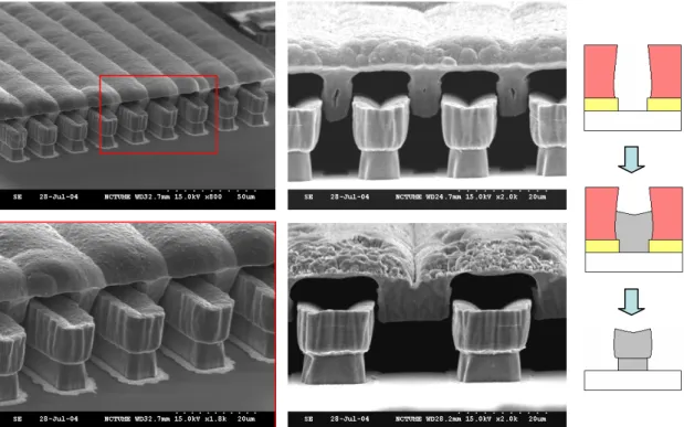
由於電鑄金屬製程除了具低溫的特性外,亦 有其製程獨特性,此獨特性在製作懸浮結構上是 現有矽基微加工製程所無法達成的。利用此特性 可提供垂直空間式金屬犧牲層製程(VSMSL)的技 術需求,藉此可達成固定金屬微結構與懸浮金屬 微結構垂直交錯之目的,也就是垂直式梳狀致動 器之製作需求。圖 4 顯示 VSMSL 製程的設計概 念,犧牲層與結構層為不同金屬,其中犧牲層 1 與 2 的設計可提供懸浮結構進行出平面運動之運 動空間,犧牲層 3 則提供固定結構與可動結構之 間的間隙控制,此間隙大小直接影響到靜電驅動 力的大小,最後的金屬回填則可完成懸浮結構之 製作。此一製程技術所用光阻可為正光阻或負光 阻,其中正光阻將用 AZ 系列,受限於其厚度特 性,至多僅能達數十微米,負光阻將用 SU-8,厚 度可達數百微米,將搭配嵌入法進行製作。 圖 4 VSMSL 製程之設計概念,可提供垂直交錯 結構之製造。 圖 5 為 VSMSL 製程的流程圖,首先在非導 體基材上以濺鍍或蒸鍍沈積電鑄起始層,然後以 第一道光罩定義光阻圖案,接著以此光阻作為電 鑄模,電鑄犧牲層 1 之金屬結構,圖 5(a)。接著 塗佈更厚的光阻,再以第二道光罩定義此光阻圖 案,作為下電極結構及犧牲層 2 之電鑄模,圖 5(b)。然後依序先進行下電極結構之電鑄製程, 獲得所需結構高度後,再接著進行犧牲層 2 之電 鑄步驟,圖 5(c)。以第三道光罩定義光阻圖案, 進行犧牲層 3 之電鑄步驟,經由此電鑄膜厚控制 上下電擊之間的間隙大小,圖 5(d)。以第四道光 罩定義光阻圖案,進行懸浮金屬結構之電鑄回填 步驟,圖 5(e)。最後移除犧牲層,釋放懸浮結 構,圖 5(f)。 由於使用 AZ 系列正光阻時,其深寬比性能 表現遠不如 SU-8,故可利用背向曝光的方法增進 正光阻的深寬比,以獲得較佳的製作結果。因 此,結合背向曝光之方法可獲得一個改善過後之 製程,相較於原來的製程,新製程中的犧牲層 1 與下電極結構具有自我對準的機制,因此光罩數 目可減少一道。製作流程如圖 6 所示,首先在玻 璃基板上利用濺鍍製程沈積厚度為 1000/200Å的 電鑄起始層 Cu/Ti,然後電鑄 Cu 作為犧牲層 1, 圖 6(a)。接著去除電鑄起始層以進行後續的背向 曝光,圖 6(b)。然後旋塗厚膜正光阻進行背向曝 光,圖 6(c)。利用電子束蒸鍍系統沈積電鑄起始 層 Ni/Cr,圖 6(d) ,此步驟需減少側壁附著。接 著電鑄下電極結構與犧牲層 2,圖 6(e)。去除厚 膜正光阻後,圖 6(f),電鑄犧牲層 3 以分開上下 電極結構,圖 6(g)。然後以電鑄製程進行上電極 結構回填,圖 6(h),再電鑄可撓樑作為可動結構 的彈簧支撐(spring),使結構得以懸浮,圖 6(i)。 最後經過蝕刻釋放可獲得懸浮結構,圖 6(j)。 圖 5 VSMSL 製程之製造流程 (a)電鑄 Cu (b)光阻 圖刻 (c)電鑄 Ni 與 Cu (d)電鑄 Cu (e)電鑄 Ni (F)釋 放結構 圖 6 改善後之 VSMSL 製程 (a)電鑄 Cu (b)去除種 子層 (c)背向曝光 (d)沈積 Ni/Cr (e)電鑄 Ni 與 Cu (f)去除光阻 (g)電鑄 Cu (h-i)電鑄 Ni (j)釋放結構 犧牲層 1 犧牲層 3 犧牲層 2 (a) (b) (c) (d) (e) (f)
四
四
四
四、
、
、
、驗證
驗證
驗證
驗證
在實驗結果的部分,包含利用方形微結構對 嵌入法進行驗證,並詳細探討各項尺寸對嵌入效 果的影響,以及可提供製作相互垂直交錯的懸浮 金屬結構之 VSMSL 製程開發結果。 1 嵌入法改善效果嵌入法改善效果嵌入法改善效果 嵌入法改善效果 本計畫用以研究嵌入法特性的 SU-8 光阻厚 度皆固定在 300 微米,使用表 2 所列的微影製程 參數可獲得最佳線寬 20 微米的 SU-8 電鑄模,深 寬比可達 15。然而當 SU-8 電鑄模的間隔小於 40 微米時,顯影液很難流入深的溝槽裡面,因而造 成底部光組無法被清除乾淨,因此 SU-8 電鑄模 的最小間隔為 40 微米,而電鑄金屬結構的最小 線寬 w 也將被限制在 40 微米。圖 7(a)所顯示的 SEM 照片是最佳線寬 20 微米的 SU-8 電鑄模,而 圖 7(b)是成功電鑄完成並去除電鑄模的金屬結 構,其線寬為 40 微米。圖 8 顯示了在沒有使用 嵌入法的狀況之下,當使用 SU-8 去除液去除電 鑄模時,常發生的兩個典型問題。圖 8(a)顯示了 在電鑄之前的電鑄模,其厚度 h 為 300 微米,寬 度 w 為 80 微米,間隔 s 為 40 微米。圖 8(b)顯示 了在電鑄之後,對於厚度為 200 微米的金屬結 構,電鑄模的碎片常殘留在基材上,特別是陷在 (a) (b) 圖 7 (a)最佳解析度之 SU-8,厚度 300 微米,線 寬 20 微米 (b)高度 200 微米,寬度 40 微米之 Ni 結構。 (a) (b) (d) 圖 8 未使用嵌入法 (a)電鑄前的 SU-8 電鑄模 (b)脫 膜後 SU-8 殘留 (c)脫膜後結構剝落損毀 金屬與金屬之間的間隙中。圖 8(c)顯示了另一個 問題,在去除電鑄模的過程中,當電鑄起始層與 金屬結構介面間的黏著力不足以抵抗脫模的力量 時,有些金屬結構會從基材上被剝落下來。 利用 SU-8 建構金屬結構時,可使用兩個主 要的手段以減少製程的失敗,包含降低金屬高度 以及嵌入法的使用。降低金屬高度可減少脫模過 程中光阻對金屬所產生的剝離力量,同時去除液 也更容易滲入光阻底部,使脫模過程容易完成。 使用嵌入法則可增加金屬結構對脫模力量的抵抗 能力,當使用超音波震盪協助光阻脫落時,嵌入 基材的根部(root)不但使金屬結構與基材的附著性
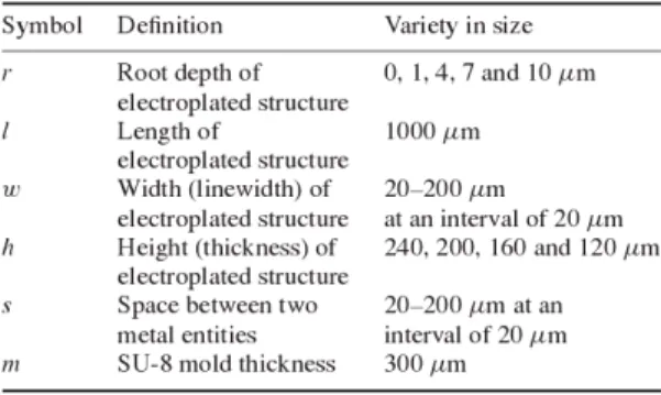
圖 9 使用嵌入法成功電鑄 Ni 結構並完成脫膜 (a)結構高度 160 微米,嵌入深度 7 微米 (b)結構高度 120 微 米,嵌入深度 1 微米。 (a) (b) (c) (d) 圖 10 嵌入深度 r,線寬 w,間隔 s 與電鑄結構高度 h 之間的關係 (a)h/m=0.80 (b)h/m=0.67 (b)h/m=0.53 (b)h/m=0.80 (a) (b)
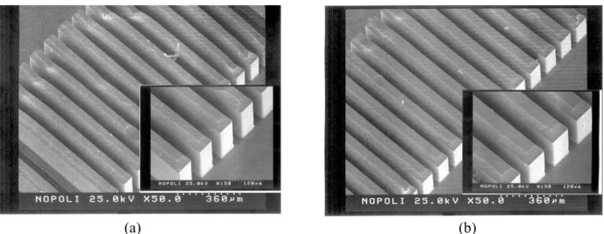
大幅提高,也讓金屬結構更不易因超因波震盪而 損毀。如圖 9 所示,使用與圖 8(a)相同幾何尺寸 的 SU-8 電鑄模以及嵌入法,可成功電鑄金屬結 構並完成脫模。圖 9(a)顯示高度 160 微米,寬度 80 微米,嵌入深度 7 微米的金屬結構。圖 9(b)顯 示高度 120 微米,寬度 80 微米,嵌入深度 1 微米 的金屬結構,當降低結構高度時,所需的嵌入深 度也大幅降低。 2 嵌入深度與幾何尺寸的關係嵌入深度與幾何尺寸的關係嵌入深度與幾何尺寸的關係 嵌入深度與幾何尺寸的關係 圖 10 總結了嵌入深度 r,線寬 w,間隔 s 與 電鑄結構高度 h 之間的關係。SU-8 電鑄模的厚度 m 為 300 微米,電鑄結構高度分別為 240、200、 160 與 120 微米,根據 h/m 的值,實驗數據可被 分成四群。如圖 10(a)與(b)所示,對於高度較高 (即 h/m 的值為 0.80 或 0.67)的金屬結構而言,即 使使用超音波震盪協助脫模,交鏈過後的 SU-8 仍舊非常難以去除。當 h/m 的值為 0.80 時,圖 10(a),可達到的最小線寬為 120 微米,其中間隔 s 為 200 微米,嵌入深度至少 4 微米。較高的 h/m 值會造成脫模困難,嵌入深度 r 的增加並不能有 效解決光阻陷在金屬中間而無法脫落的問題。然 而,增加間隔 s 的大小則可有效降低金屬結構的 寬度,如圖 10(b)所示,當結構高度為 200 微米 時(h/m = 0.67),較大的間隔 s 可獲得較小的金屬 線寬 w,也就是說,在有限的面積裡面(w+s = constant),線寬 w 與間隔 s 有明顯的 trade-off 關 係。 對於高度較低(即 h/m 的值為 0.53 或 0.40)的 金屬結構而言,在脫膜過程中最主要的失敗狀況 是金屬結構的剝離損毀,嵌入深度的增加可幫助 結構有效保留在基板上。圖 10(c)顯示嵌入深度 r 對線寬 w 的縮小有明顯的效果,對結構高度為 160 微米(h/m = 0.53)的金屬結構而言,當間格 s 為 80 微米(曲線 D)且嵌入深度為 0、1 與 4 微米 時,金屬結構所能達到的最小線寬分別是 200、 140 與 80 微米。在曲線 D 中,嵌入深度為 4 微米 的金屬結構,其最小線寬比未使用嵌入法的狀況 縮小了 2.5 倍。當間格 s 增加為 160 與 200 微米 且嵌入深度為 4 微米時,最小線寬可進一步縮小 到 60 與 40 微米,如圖 10(c)曲線 B 與 A 所示。 圖 10(d)顯示了更低的金屬結構(高度 120 微米, h/m = 0.40)使用嵌入法的狀況,由於金屬結構較 低,僅需 1 微米的嵌入深度便可使各種不同間格 大小的結構達到 40-60 微米的最小線寬。因此在 h≤120 微米,s≥60 微米,m = 300 微米的狀況 下,1 微米的嵌入深度對結構抵抗脫膜力量是最 有效率的。 雖然嵌入法可有效幫助結構抵抗脫膜力量使 結構較不易剝落,但卻無法有效改善光阻陷在金 屬結構之間的狀況。因此當電鑄結構高度很接近 SU-8 的厚度時,如圖 10(a)與(b)的狀況(h/m = 0.8 與 0.67),嵌入法對縮小線寬的改善並不明顯,主 要原因是殘留光阻陷在金屬之間的間隙中而造成 製程的失敗。 此外我們展示了利用電鑄高度 h 與 SU-8 膜 厚 m 的比值以及圖 10 的相關資料,可幫助選擇 需要的製程參數以成功製造各種不同厚度的金屬 線圈結構。圖 11(a)與(b)顯示了在沒有使用嵌入 法的狀況下,因光阻的殘留以及金屬結構的剝落 損壞造成製程的失敗。圖 11(c)則顯示了利用嵌入 法成功製造了 Ni 金屬線圈,其中 Ni 線圈的高度 h 為 200 微米,線寬 w 為 80 微米,間格 s 也是 80 微米。當使用 400 微米厚度的 SU-8 時,h/m 的值 為 0.5,因此可參考圖 10(c)曲線 D,其中 s 為 80 微米,w 為 80 微米,4 微米的嵌入深度即可滿足 製造所需要的 Ni 線圈。 (a) (b) (c) 圖 11 鎳線圈製作,高度 200 微米,線寬 80 微 米,間隔 80 微米 (a)光阻殘留 (b)結構損毀 (c)成 功脫膜
3 VSMSL 製程製作結果製程製作結果製程製作結果製程製作結果 為了簡便製程開發的過程起見,VSMSL 製 程的開發將由較易處理的 AZ 系列正光阻開始測 試,而為了改善正光阻的製作效果,因此在此將 優先測試改善過後的製程(如圖 6 所示)。在此製 程中,電鑄銅與電鑄鎳將被使用當作犧牲層與結 構層,兩款常見的商用正光阻 AZP 4620 與 AZ 9260 將被使用當作電鑄模。圖 12 顯示了所設計 用來開發製程的相關幾何尺寸,上梳狀結構與下 梳狀結構的指寬度分別是 4-14 微米與 8-15 微 米,上下指之間的間隙(gap)是 3 微米,可動行程 為 12.5 微米,上下梳狀結構重疊距離為 5 微米。 圖 12 VSMSL 製程相關尺寸 圖 13 為背向曝光過後(圖 6(c)所示步驟)光阻 結構的 SEM 照片,由圖 13(a)可知,AZP 4620 會 因為繞射效應(differation)在顯影過後產生嚴重的 內縮現象,這不但會影響下梳狀結構的外型,也 會讓後續製程容易失敗。相較之下,AZ 9260 則 提供了良好的光阻外型,圖 13(b),並使後續製 程的良率(yield)大幅提昇。例如,在圖 6(e)所示 的製程步驟中,若使用 AZP 4620,該步驟的良 率約為 5%-10%,若使用 AZ 9260,良率則大幅 提昇至 90%以上。 在交錯電鑄銅與鎳並完成所有電鑄製程之 後,玻璃晶片便由切割機進行切割,然後使用 NH4OH+H2O2溶液作為蝕刻液進行最後的結構釋 放(release)。圖 14 顯示了採用 AZP 4620 作為電 鑄模的製作結果,在背向曝光中產生嚴重內縮的 光阻結構造成了齒狀的下梳狀結構。同時,當溝 槽(trench)的寬度較窄的時候,電鑄鎳回填的過程 中,鎳將很難完全填滿整個溝槽而留下孔洞,當 溝槽的寬度較寬時,則可有效消除孔洞。齒狀的 梳狀結構會使致動器的效能大幅降低,AZ 9260 的良好特性則可有效幫助消除齒狀外形,如圖 15 所示,在採用 AZ 9260 作為電鑄模後,下梳狀結 構獲得較佳的垂直度。然而,齒狀外形已獲得改 善,但可動梳狀結構與固定梳狀結構卻相互沾黏 在一起,甚至在釋放的步驟進行了七天之後,仍 舊無法將上下梳狀結構互相分離。因此,為了製 圖 13 背向曝光並顯影過後之光阻結構 (a)光阻 AZP 4620 製作結果 (b)光阻 AZ 9260 製作結果 5 unit: μm (a) (b) AZP 4620 AZ 9260 AZP 4620 AZ 9260
圖 14 採用 AZP 4620 作為電鑄模的製作結果,在背向曝光步驟中因光阻嚴重的內縮造成齒狀結構。
圖 15 採用 AZ 9260 的製作結果,明顯減少因繞射造成的光阻內縮現象,大幅降低了齒狀結構的產生。
圖 16 增加第三層犧牲層 Cu 的厚度 (a)Cu 厚度增加為 4-6 微米 (b)Cu 厚度增加為 6-8 微米 (a) (b)
作所需要的間隙使上下結構互相分離,便將第三 層銅犧牲層的厚度增加為 4-6 微米以及 6-8 微 米。然而,如圖 16 所示,可動梳狀結構仍舊沾 黏在固定梳狀結構上,當第三層銅犧牲層的厚度 增加時,銅金屬並未如預期均勻地沈積在整個溝 槽中,而是集中沈積在下梳狀電極的頂端,如圖 17 所示,如此將無法成功透過銅犧牲層的沈積將 上下梳狀電極分開。因此,若要克服此問題,必 須先改善電力線集中在金屬頂端而造成沈積速度 不均勻的問題。 圖 17 因電場集中,電鑄 Cu 集中沈積在下梳狀電 極的頂端。
五
五
五
五、
、
、結
、
結
結論
結
論
論
論
本計畫分別是利用正光阻進行 VSMSL 製程 的開發以及利用 SU-8 光阻進行嵌入法的特性分 析,以增進 VSMSL 製程在深寬比上的製作效 果。 對於嵌入法的特性調查,我們對 SU-8 光阻 建立了具參考價值的資料庫,透過測試結構的製 造可瞭解到電鑄結構嵌入深度、線寬以及厚度之 間的關係。不同的根部深度可透過 SiO 遮罩與 KOH 蝕刻進行製造。對較低 h/m 值(0.54 或 0.40) 的金屬結構而言,嵌入法可有效地解決在脫膜過 程中結構剝落損壞的問題。以鎳線圈的製作為 例,利用 4 微米的嵌入深度以及 400 微米厚的 SU-8,可成功製造厚度 200 微米、線寬 80 微米 的線圈。若以傳統的方法製作相同線圈,厚度僅 能達到 50 微米。因此嵌入法可有效改善採用 SU-8 光阻製作固定金屬結構可達到的深寬比,這對 VSMSL 製程在製程能力上將有所助益。 在梳狀懸浮金屬結構的製作上,採用正光阻 AZ 9260 可獲得較佳的側壁垂直度,不但可提升 製程良率,亦可有效避免在背向曝光時因繞射而 導致光阻嚴重內縮的情形。然而以電鑄製程在金 屬溝槽中沈積作為犧牲層的銅膜以分開上下梳狀 結構的時候,因為電力線的集中而導致電鑄銅亦 集中沈積在下梳狀結構的頂端,這使得電鑄銅膜 無法均勻地分佈在金屬溝槽中,因而造成上下梳 狀結構無法分開。在後續的研究中,將嘗試採用 具有良好填洞能力的 super-filling 銅電鍍技術, 可避免底端沈積速率較慢的問題;或者採用電漿 輔助化學氣相沈積系統(PECVD)低壓的環境沈積 SiO2取代電鑄銅膜作為犧牲層,以提供較佳的膜 厚均勻性。 References1. Beak, C. –W. and Kim, Y. –K., “Novel Fabrication Process of Freestanding Metallic
Microstructures Using Double Electroplating”, J. J. Appl. Phys., Vol. 37, pp. 7104-7109, 1998 2. Chatzichristidi, M.; Raptis, I.; Diakoumakos, C.
D.; Glezos, N.; Argitis, P. and Sanopoulou M., “Strippable Aqueous Base Developable Negative Photoresist for High Aspect Ratio Micromachining”, J. Microelectronic Engineering, 61-62, pp. 729-735, 2002
3. Conèdèra, V.; Goff, B. Le. and Fabre, N., ”Potentialities of a New Positive Photoresist for the Realization of Thick Moulds”, J. Micromech. Microeng., No. 9, pp. 173-175, 1999 4. Hirano, T.; Fan, L. –S.; Gao, J. –Q. and Lee, W.
Y., “MEMS Milliactuator for Hard-Disk-Drive Tracking Servo”, Journal of Microelectromechanical Systems, Vol. 7, No. 2, pp. 149-155, 1998
5. Ho, C. –H.; Chin, K. –P.; Yang, C. –R.; Wu, H. – M. and Chen, S. –L., “Ultrathick SU-8 Mold Formation and Removal, and Its Application to the Fabrication of LIGA-like Micromotors with Embedded Roots”, Sensors and Actuators A, 102, pp. 130-138, 2002
6. Lorenz, H.; Despont, M.; Fahrni, N.; Brugger, J.; Vettiger, P. and Renaud, P., “High-aspect-ratio, Ultrathick, Negative-tone Near-UV Photoresist and Its Applications for MEMS”, Sensors and Actuators A, 64, pp. 33-39, 1998
7. Miyajima, H. and Mehregany, M., “High-Aspect-Ratio Photolithography for MEMS Applications”, Journal of Microelectromechanical Systems, Vol. 4, No. 4, Dec. 1995
8. Qu, W.; Wenzel, C. and Gerlach, G., “Fabrication of a 3D Differential-capacitive Acceleration Sensor by UV-LIGA”, Sensors and Actuators A, 77, pp. 14-20, 1999
9. Roth, S.; Dellmann, L.; Racine, G. –A. and Rooij, N. F. de, “High Aspect Ratio UV Photolithography for Electroplated Structures”, J. Micromech. Microeng., No. 9, pp. 105-108, 1999 10. Tseng, F. –G. and Yu, C. –S, “High Aspect
Ratio Ultrathick Micro-stencil by JSR THB-430N Negative UV Photoresist”, Sensors and Actuators A, 97-98, pp. 764-770, 2002
11. Yoon, J. –B.; Kim, B. –I.; Choi, Y. –S. and Yoon, e., “3-D Construction of Monolithic Passive Components for RF and Microwave ICs Using Thick-Metal Surface Micromachining Technology”, IEEE Transactions on Microwave Theory and Techniques, Vol. 51, No. 1, pp. 279-288,Jan. 2003
12. Yoon, J. –B.; Han, C. –H.; Yoon, E. and Kim, C. –K., “Monolithic Integration of 3-D Electroplated Microstructures with Unlimited Number of Levels Using Planarization with A Sacrificial Metallic Mold (PSMM)”, Twelfth IEEE International Conference on Micro Electro Mechanical Systems, 1999, 17-21 Jan. 1999
出席國際學術會議報告
會議名稱:2005 年微機電系統研討會
MEMS 2005
The 18
thInternational Conference on Micro Electro Mechanical Systems
時間:2005 年 1 月 30 日至 2 月 3 日
地點:美國 邁阿密 Miami, USA
報告人:交通大學機械系 徐文祥 教授
一、 會議內容
此 MEMS 研討會是每年舉辦一次的國際性研討會,輪流在歐洲,
美洲,及亞洲舉辦,是微機電系統領域最知名的國際學術會議,其第
一屆是 1987 年開始,而今年是第十八屆,此會議的傳統特色是
single-session format,也就是同一時段僅有一個 session 在進行,所以
聽眾不會有顧此失彼之虞,但也正因為如此,此會議論文接受率可能
是所有國際會議最低的,以今年為例,共有 750 篇論文投遞,但僅接
受 216 篇論文,接受率約為 29%,可能比許多期刊論文接受率都低,
其 中 包 含 41 篇 oral papers 及 175 篇 poster paper , 會 議 主 席 為
University of Colorado 的 Dr. Victor M. Bright 及 Carnegie-Mellon
University 的 Dr. Gary K. Fedder,整個負責論文審查的 Technaical
program committee 共有 21 位,我國是由清大范龍生教授代表。而
2006 年將在土耳其伊斯坦堡舉辦。
本 屆 會 議 將 41 篇 口 頭 報 告 論 文 分 為 9 個 sessions , 216 篇
poster/oral 論文安排在 4 個時段交流,其中 oral session 的主題分別為
1. Selfassembly and Packaging
2. RF MEMS
3. Pneumatic/Jet Systems
4. Optical Microsystems
5. Power MEMS
6. Physical Microsystems
7. Polymer MEMS
8. Bioanalytical Systems
9. Nano Systems
另安排了三個 Invited talk,分別是
Jan. 30. Microfabricated Atomic Clocks,
J.Kitching, S. Knappe, L. Liew, P. Schwindt, V. Shah, J. Moreland and L.
Holleberg, The National Institute of Standards and Technology and University
of Colorado, USA
Feb. 1. Liquid Lens Technology : Principle of Electrowetting
Based Lenses and Applications to Imaging,
1. B. Berge, Varioptic, France
Feb. 2. Micromachining/Nanotechnology in Direct Methanol Fuel Cell
E. Sakaue, Toshiba, Corporation, Japan
可以發現傳感器及微機電系統的研究趨勢,在尺度上,正逐步由微米
擴展至奈米,在領域上,由傳統工程拓展至分子生物科學,在發展目標
上,從創新概念邁向實際應用。
二、 參加會議經過
此次會議是在Miami Beach的Fontainebleau Hilton Resort舉行,我國
被接受的論文共有5篇,皆是海報展示論文。除交大外,尚有台大,工研
院,逢甲及一篇清大動機方維倫老師博士班學生透過千里馬計畫,在美國
Carnegie-Mellon University Professor Fedder 實驗室所作的加速度計
口頭報告論文。
本人的論文是安排在2月1日下午作展示與報告,題目是Nanocomposite
Effects on the Coefficient of Thermal Expansion Modification for
High Performance Electro-thermal Microactuator,主要是報告我們在
電鍍製作金屬微結構時,加入鑽石奈米粒子,發現材料性質的變化,尤其
是可提升熱膨脹係數,故可應用在微熱致動器中。由於此會議的Poster
session的安排方式不僅是海報展示,在特定的兩個小時中,還需在論文
前做三次約十分鐘的口頭報告,以方便聽眾在特定時間到有興趣的論文前
聽口頭說明。由於作者就在其論文前,通常有疑問就可直接與作者請教,
交流效果比口頭論文提問還好。就此次會議內容而言,美國、日本、韓國
感覺論文最多,歐洲論文也佔約1/3,但似乎沒有哪一國家特別多,而日
本及韓國的論文常是與企業合作,所以系統化程度較佳,而趨勢來看,此
次較不感覺有很新奇的創新應用,而是較紮實的改進式論文較多,顯示微
機電系統的研發在這些國家中已較普遍的由學校拓展至產業界。在2日晚
上,大會並安排了Evening Banquet,大家在輕鬆的狀態下交流,在樂隊
伴奏下用餐,與許多老朋友相聚及認識一些新朋友,十分難得。
三、 與會心得
參與此次會議,深感所發表論文水準廣度及質量皆佳,參與者多
來自世界各國發展微機電領域的主流單位,即使是海報展示論文也多
極具水準,尤其在海報論文展示時段負責解說的作者,常多是教授而
非學生,顯示大家對此會議的重視,而且海報展示時也有較充裕的時
間與作者討論,感覺上有時比去聽口頭報告論文收穫更多。
此次感謝國科會補助,能讓我順利成行,此次會議由於內容豐
富,邁阿密的市區也未能抽出時間瀏覽,雖有些可惜,但參與此次會
議,讓本人能暫時從每日繁忙的工作中抽出身來,而專心在此一高水
準會議中進行交流及學習,感覺十分充實。
四、攜回資料
1. 會議議程一本
2. 論文集及論文光碟一片
3. 廠商產品資料
15
Nanocomposite Effects on The Coefficient of Thermal Expansion Modification for High
Performance Electro-Thermal Microactuator
1,2
Li-Nuan Tsai,
1Y-T Cheng, and
2Wensyang Hsu
1Microsystems Integration Laboratory,
Department of Electronics Engineering,
National Chiao Tung University
2
Department of Mechanical Engineering, National Chiao Tung University
1001 Ta Hsueh Road, Hsinchu, Taiwan, 300, ROC
*[email protected]
ABSTRACT
We employ a low-temperature stress-free electroplated nickel (EL) process with the addition of uniformly dispersed nanoparticles of diamond (< 500 nm) or SiO2 (< 80 nm) to
investigate “nanocomposite effects” for the first time on the modification of the thermal expansion coefficient (CTE) and other mechanical properties of nickel and its correlation to power and reliability improvement of electro-thermal microactuators. Experimental results show that these material parameters can be either enhanced or deteriorated via the incorporation of different kind of nanopowders. Although the mechanical strength enhancement can be attributed to the intrinsic characteristics of the nanoparticle based on the rule of mixture, the discrepancy of CTE modification can only be explained with distinct composite microstructures which result in the performance improvement of the electro-thermal microactuator. This work has led to a possible research direction in the development of MEMS using the nanocomposites.
1. INTRODUCION
For the development of cost effective, highly integrated MEMS, electro-deposition technique is a manifest choice for device fabrication since as-plated nickel metal has comparable mechanical properties with polysilicon, lower electrical and thermal resistivity, higher deposition rate (>10mm/hr) and lower processing temperature (around room temperature) in general. Meanwhile, recent investigations in the nanocomposite syntheses and characterizations show that the intrinsic physical property limits of metal, including hardness, Young’s modulus, and coefficient of thermal expansion (CTE)…etc. [1-5], can be further modified and strengthen via the incorporation of well distributed ceramic nanopowders like Al2O3, SiC, Si3N4, and diamond. Thus,
employing the nanocomposites synthesized by electro-deposition process for MEMS fabrication has revealed its excellent prospect.
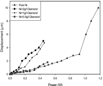
Previously, our research group already demonstrated several Ni based nanocomposite synthesis methods and MEMS devices made of the composites [5-7]. For electro-thermal microactuator application, it is found that the microactuator made of Ni/nano-diamond composite film (0.248 W) can reduce 73 % power requirement of a pure nickel device (0.924 W) for the same 3 µm displacement as shown in Fig. 1 [6]. Meanwhile, in comparison with the pure nickel one, which exhibits 1.8 µm reversible
deformation, the microactuator made of the Ni/nano-diamond composite can exhibit better performance that is over 3 µm. Although the power and reliability enhancements can be attributed to nanocomposite effects on the modification of metal property, it is still required to further investigate the correlation between the effects and device performance, especially while the present studies mainly focus on the property characterizations of the composites in either bulk form or thin film appearance.
The CTE (Coefficient of Thermal Expansion) of a nanocomposite is very important to MEMS fabrication. During the deposition of composite film, process temperature variation from a higher point to lower one will result in the formation of thermal stress between the film and its underneath silicon substrate due to the CTE difference, which could cause thin film delamination or deform subsequent device structure that made of the film. On the other hand, electro-thermal microactuator can have larger displacement while it is made of the material with higher CTE coefficient [6]. Thus, this work will attempt an investigation of “nanocomposite effects” for the first time on the modification of CTE and other mechanical properties of nickel which results in the power and reliability improvement of the electro-thermal microactuator. We hope that, via the understanding of the correlation, such a nickel nanocomposite not only fascinates high performance electro-thermal microactuator fabrication but also leads an alternative direction in the development of MEMS fabrication based on the use of nanocomposite effects.
2.
FABRACTION PROCESS
In the experiment, we utilize cantilever beam and electro-thermal microactuator for the characterization and investigation of the nanocomposites and related device performance. The material synthesis is based on a low-temperature stress-free electroplated nickel (EL) process with the addition of uniformly dispersed nanoparticles of diamond or SiO2 whose sizes are smaller than 500 and 80nm,
respectively. SiO2 nanopowder is chosen for the comparison
purpose in this experiment due to its lower CTE value than that of Ni and diamond. The amount of the particle incorporation is controlled using different plating bath with different concentration.
Figure 2 shows the fabrication process of the cantilever beams. The device first comes with a 1µm thick photoresist coating on a silicon wafer as a sacrificial layer, which is followed by a thin Ti/Cu films (100Å/1000Å) deposition as
an adhesion and seed layer, respectively, as shown in Fig. 2(b). Another 7µm photoresist is then utilized as an electroplating mold as shown in Fig. 2(c). After that, Ni or Ni based nanocomposite films are electroplated at 50℃ to form the micro cantilevers as shown in Fig. 2(d). Finally, the cantilever is formed after stripping its underneath sacrificial layer. The fabrication process of the electro-thermal microactuators is similar except that a 2 µm SiO2
instead of the photoresist is deposited for electrical isolation and as a sacrificial layer.
3. RESULTS AND DISCUSSIONS
SEM micrographs of the as-fabricated cantilever beam array and electro-thermal microactuator which made of pure Ni and Ni-diamond nanocomposites, respectively, are shown in the Fig. 3. The microactuator has similar surface morphology to that of cantilever beam. In addition, no bend up or down phenomenon has been found in these structures. These results indicate that the newly developed stress-free nanocomposite synthesis can provide as good as conventional electroplating process for MEMS device fabrications.
Fig. 1. Applied powers versus displacements of microactuators at different incorporation of diamond nanoparticle concentrations.
Fig. 2. Fabrication process of the nanocomposite cantilever beam using metal-based surface micromachining process.
Nano-indentor is first applied to characterize the hardness and Young’s modulus of nanocomposite films. As shown in Fig. 6(a), we found that with the increasing diamond concentration, Young’s modulus of the Ni-diamond nanocomposite cantilever with 2g/l diamond particles is larger than pure nickel cantilever 1.2 times. On the other hand, Young’s modulus of nickel matrix contains SiO2
nanoparticles is down from 190.6GPa to 180GPa. Figure 6(b) shows that the hardness increases with the concentration of the diamond nanoparticles in the plating bath. The hardness enhancement can be attributed to the incorporation of diamond nanoparticle. However, in comparison with diamond, the incorporation of SiO2
nanopowders into nickel matrix, the hardness is decreased from 4.56GPa to 3.82GPa. The degradation can be expected due to lower mechanical strength of SiO2. Accordingly,
both Young’s modulus and hardness can be evidently enhanced or degraded by embedding the diamond or silica nanoparticles in the nickel matrix, respectively.
In addition to the mentioned mechanical properties, CTE is also an important parameter directly affecting on electro-thermal microactuator performance. In order to calibrate the CTE of electroplated Ni-diamond and Ni- SiO2 films, an in–
house CTE measurement appearances is used here. By calibrating the elongation of the cantilever in the heated chamber with temperature control, the thermal expansion coefficients at different temperatures can be obtained using Eq. (1). T L L L T ∆ ⋅ − = ( ) 1 ) ( 0 0 1 1 α (1)
whereL is the length at temperature1 T , 1 L is the initial 0 length at temperatureT , and 0 ∆T =T1−T0.
Figure 4 and 5 show the measured CTEs of the nanocomposites plated with different concentrations of diamond and silica nanoparticle incorporations at 400 ℃ , respectively. The CTE values increase with the concentration of diamond nanoparticle starting from 27×10
-6
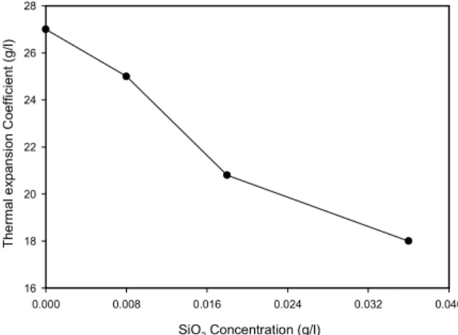
/℃ of pure nickel to 54 ×10-6/℃ of the nanocomposite plated in a bath with 2g/L of diamond nanoparticle, which is about two times enhancement. In contrast, the CTE value decreases with the concentration of SiO2 nanoparticles in the
plating bath from 27×10-6/℃ down to 18×10-6/℃ (0.036g/L). Although the mechanical property modifications could be attributed to the composite effect [5] resulted from the incorporation of diamond or SiO2 particles, which has much
higher or lower Young’s Modulus and hardness than pure nickel, the CTE increment cannot be well explained in the case of Ni-diamond nanocomposite systems due to much smaller CTE value of diamond. Hence, the microstructures of both Ni-diamond and Ni-SiO2 nanocomposites are
examined by TEM. According to the TEM analysis, as shown in Fig. 7, the dark field image indicates the nanodiamonds only distribute along grain boundary regions of nickel matrix. Figure 8 shows similar phenomenon occurring in the synthesis of Ni- SiO2 composite except that
the nanoparticles are also embedded inside nickel grains,
Power (W) 0.0 0.2 0.4 0.6 0.8 1.0 1.2 D is p la c e m e n t (µ m ) 0 2 4 6 8
10 Pure NiNi+2g/l Diamond
Ni+1g/l Diamond Ni+0.5g/l Diamond
17 which could be the deterministic factor to cause the distinct CTE behavior. Further study is required.
(a) (b)
Fig. 3. SEM of the fabricated electrolytic (a) pure Ni cantilever beam (b) electro-thermal microactuator (Ni+2 g/L diamond nanoparticles).
Fig. 4. The CTE variations at 400℃ in various diamond nanoparticles concentrations.
Fig. 5. The CTE variations at 400℃ in various SiO2
nanoparticles.
Fig. 6. A Comparison of the material properties of various material (a) Young’s modulus (b) hardness.
Fig. 7. TEM of the fabricated electrolytic Ni-diamond (2g/l) microactuator and the diamond nanoparticles entrap inset the grain boundary.
Fig. 8 TEM of the fabricated electrolytic Ni-SiO2 (0.036g/l) microactuator and the SiO2 nanoparticles entrap inset the grain.
ANSYS 6 is utilized to simulate the electro-thermo-mechanical behavior, where the element type of solid 5 is applied for the analysis. The material properties of the nanocomposite, such as the thermal conductivity and specific heat capacitance, are assumed to be the same as those of pure nickel. In addition to the CTEs determined from our CTE measurement results, the related data about the mechanical and thermal properties of Ni, Ni-diamond
(a) (b) Diamond Concentration (g/l) 0.0 0.5 1.0 1.5 2.0 2.5 T h e rm a l E x p a n s io n Co e ff ic ie n t ( p p m / ) ℃ 25 30 35 40 45 50 55 60 SiO2 Concentration (g/l) 0.000 0.008 0.016 0.024 0.032 0.040 T h e rm a l e x p a n s io n C o e ff ic ie n t (g /l ) 16 18 20 22 24 26 28 diamond nanoparticles
and Ni-SiO2 nanocomposite of the microactuators for
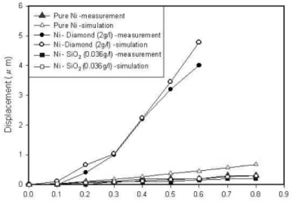
numerical analysis are listed in Table 1 [8, 9]. According to the simulation results, the relation between output displacement and input voltage is closely fitted with experimental data as shown in Fig. 9 indicating that CTE has the direct effect on the electro-thermal microactuator displacement. With the increasing concentration of diamond nanoparticles in nickel electroplating solution, CTE becomes larger as well as the output displacement of the thermal microactuators. On the other hand, the electro-thermal microactuator made of Ni-SiO2 nanocomposite with the same dimension could only provide smaller displacement due to its decreased CTE. Though it has been found that the performance enhancements of electro-thermal microactuator can be realized using nanocomposite due to its larger CTE and stronger hardness, the effects on the device originated from the change of thermal conductivity and specific heat capacitance still require further investigation.
Fig. 9. Comparison of the experimental data with finite element analysis for displacement at different applied voltage in various nanoparticle concentrations. Table 1. Material properties used in simulations [8,9]
4. CONCLUSION
This paper reveals several new composite effects on the material property modification, especially on coefficient of thermal expansion, based on the incorporation of diamond or SiO2 nanoparticles in the grain boundary of nickel matrix by
a low temperature CMOS compatiable process, which not only makes the nickel nanocomposite attractive for high- performance electro-thermal microactuators, but also may
provide an alternative direction in the development of other MEMS devices using the nanocomposites. However, other mechanical properties, such as thermal conductivity and specific heat capacitance, affected by using nanocomposite still require further investigation.
ACKNOWLEDGEMENTS
This work is supported by the National Science Council (Taiwan) under Grant NSC 93-2220-E-009-002 and NSC 93-2212-E-009-035, and in part by MediaTek research center at Chiao Tung University. Authors also would like to express their appreciations to the Nano Facility Center of National Chiao Tung University, Prof. Fang of National Tsing Hua University for providing technical supports and measurement facilities.
REFERENCES
[1] A.F. Zimmermann, G. Palumbo, K.T. Aust and U. Erb, “Mechanical Properties of Nickel Silicon Carbide Nanocomposites”, Materials Science and Engineering, A328, pp.137-146, 2002.
[2] M. Okumiya, Y. Tsunekawa, T. Saida and R. Ichino, ”Creation of High Strength Bonded Abrasive Wheel with Ultrasonic Aided Composite Plating”, Surface and Coatings Technology, 169-170, pp.112-115, 2003.
[3] Y. H. Choa, J. K. Yang, B. H. Kim, Y. K. Jeong, J. S. Lee, T. Nakayama, T. Sekino and K. Niihara, “Preparation and Characterization of metal/ceramic nanoporous nanocomposite powders”, Journal of Magnetism and Magnetic Material, 266, pp. 12-19, 2003. [4] C. Xia, X. Guo, F. Li, D. Peng and G. Meng, “Preparation of Asymmetric Ni/Ceramic Composite Membrane by Electroless plating”, Colloids and Surfaces A: Physicochemical and Engineering Aspects, 179, pp.229-235, 2001.
[5] K. S., Y. T. Cheng, and L. W. Lin, " Nickel Nano-Composite Film For MEMS Applications ", The 12th International Conference on Solid State Sensors, Actuators and Microsystems, Boston, June 8-12, pp.1534-1537, 2003.
[6] L. N. Tsai, G. R. Shen, Y. T. Cheng, and W. S. Hsu, " Power and Reliability Improvement of an Electro-Thermal Microactuator Using Ni-Diamond Nanocomposite ", The 54th Electronic Components and Technology Conference, June 2004.
[7] Guang-Ren Shen, Li-Nuan Tsai, Y. T. Cheng, T. K. Lin, and Wensyang Hsu, “Ni-P-CNTs Nanocomposite Film for MEMS Applications”,IEEE Conf. on Nanotechnology, München, Germany, Aug, 2004 [8] J. P. Holman, Heat Transfer, 6th Ed., New York:
McGraw-Hill, 1989.
[9] C. S. Pan and Wen Syang Hsu, "A Microstructure for in situ Determination of Residual Strain ", IEEE/ASME J. Microelectromechanical Systems, vol. 8, pp. 200-207, 1999.