evaluated to find their effectiveness for improving the immunity of CMOS ICs against the transient-induced latchup (TLU) under the system-level electrostatic discharge (ESD) test. By choosing proper components in each noise filter network, the TLU immu-nity of CMOS ICs can be greatly improved. All the experimental evaluations have been verified with the silicon-controlled rectifier (SCR) test structures and the ring oscillator circuit fabricated in a 0.25-µm CMOS technology. Some board-level solutions can be fur-ther integrated into the chip design to effectively improve the TLU immunity of CMOS IC products.
Index Terms—Board-level noise filter, latchup, SCR, system-level ESD test, transient-induced latchup (TLU).
I. INTRODUCTION
I
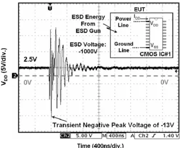
T has been a long time since latchup was a significant re-liability issue in semiconductor technologies [1]–[12]. Re-cently, the reliability issue of transient-induced latchup (TLU) has attracted more attentions than before in CMOS technol-ogy [13]–[19]. The standard practice to verify the immunity of a TLU on CMOS ICs has been announced [20]. This tendency results from not only the progress of the more integrated func-tionality into a single chip but also from the strict requirements of reliability test standards such as system-level electrostatic dis-charge (ESD) test [21] for EMC regulation. During the system-level ESD test, the electrical/electronic product must sustain the ESD level of ±8 kV (±15 kV) under contact-discharge (air-discharge) test mode to achieve the immunity requirement of “level 4.” Such high-energy ESD-induced noises, however, often cause a TLU on the electrical/electronic product, lead-ing to damage or malfunction of CMOS ICs inside the equip-ment under test (EUT). Fig. 1 shows the measureequip-ment setup of the system-level ESD test with indirect contact-discharge test mode [21]. When the ESD gun zaps to the horizontal coupling plane (HCP), all CMOS ICs inside the EUT will be disturbed due to the high ESD-coupled energy, as shown in the inset Fig. 1. The measured VDDtransient waveform on one (CMOS IC#1) of the CMOS ICs inside the EUT with ESD voltage of−1000 V zapping on the HCP is shown in Fig. 2. Clearly, the power line (VDDpin) of CMOS IC#1 no longer maintains its normal voltage level (+2.5 V) but acts as a bipolar (underdampedsi-Manuscript received August 8, 2005; revised December 6, 2005. This work was supported by Himax Technologies, Inc., Taiwan, R.O.C.
The authors are with the Nanoelectronics and Gigascale Systems Laboratory, Institute of Electronics, National Chiao-Tung University, Hsinchu, Taiwan 300, R.O.C. (e-mail: [email protected]; [email protected]).
Digital Object Identifier 10.1109/TEMC.2006.870681
Fig. 1. Measurement setup of the system-level ESD test with indirect contact-discharge test mode [21]. The ESD gun zapping on the horizontal coupling plane (HCP) could cause TLU events on all CMOS ICs inside the EUT.
Fig. 2. Measured VDDtransient waveform on one (CMOS IC#1) of the CMOS
ICs inside the EUT with an ESD voltage of−1000 V zapping on the HCP. VDD
waveform acts as a bipolar voltage due to the disturbance of the high ESD-coupled energy.
nusoidal) voltage with a transient negative peak voltage of−13 V. Such bipolar voltage on power or ground lines of CMOS ICs can easily trigger on TLU [22] to result in malfunction or dam-age in CMOS ICs, even though such TLU-sensitive CMOS ICs have already met the requirements of the quasi-static latchup test standard [23].
It has been clarified that the “sweep-back current” [22] caused by the bipolar trigger voltage on power (ground) pins of CMOS ICs is the major cause of a TLU under the system-level ESD test. TLU can be initiated by the sweep-back current when the bipolar trigger voltage on VDDincreases from its negative peak voltage to a positive voltage [22]. Such sweep-back current is strongly dependent on the related dominant parameters of the bipolar trigger voltage waveform, such as transient peak voltage, damping frequency, and damping factor [24]. In real situations, however, all these parameters depend on the charged voltage of the ESD gun, the adopted TLU test mode, metal traces of the board-level (chip-level) layout, and the board-level noise filter network where the device under test (DUT) is located, etc. Among these factors to possibly determine the occurrence of TLU, the board-level noise filter could be a dominant solution to enhance the TLU immunity of CMOS ICs, because the use of the board-level noise filter network between the noise sources and CMOS ICs can decouple, bypass, or absorb noise voltage (energy) [25], [26] which may initiate TLU. Thus, the TLU im-munity of CMOS ICs will strongly depend on the board-level noise filter network. However, so far, it has not yet been investi-gated how the board-level noise filter network can enhance the TLU immunity of CMOS ICs under the system-level ESD test. The purpose of this work is to develop a high efficiency board-level noise filter network for TLU prevention under the system-level ESD test. Different types of noise filter networks are evaluated to find their improvements on TLU immunity, in-cluding capacitor filter, ferrite bead, transient voltage suppres-sor (TVS), and several high-order noise filters such as LC-like (second-order) and π-section (third-order) filters. All the experi-mental results have been verified with silicon-controlled rectifier (SCR) test structures and the ring oscillator circuit fabricated in a 0.25-µm CMOS technology.
II. DEPENDENCIES OFBOARD-LEVELNOISEFILTERS ON
BIPOLARTRIGGERWAVEFORMUNDER THESYSTEM-LEVEL
ESD TEST
During the system-level ESD test, a board-level noise filter can enhance the TLU immunity of CMOS ICs by decoupling, bypassing, or absorbing the ESD-induced noise voltage (en-ergy), which may initiate the TLU. That is, the board-level noise filter has strong impacts on the related dominant parame-ters of the TLU-triggering voltage (bipolar trigger voltage) such as transient peak voltage, damping frequency, and damping fac-tor. To better clarify how the board-level noise filter will affect these parameters so as to further enhance the TLU immunity of CMOS ICs, we present several examples about the dependency of board-level noise filters on bipolar trigger waveform under the system-level ESD test.
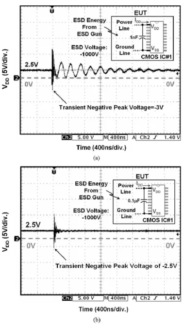
With a decoupling capacitance of 1 nF and 0.1 µF between
VDD and VSS (ground) of the CMOS IC#1 under the system-level ESD test, the measured VDDtransient waveforms with an ESD voltage of−1000 V zapping on the HCP are shown in Fig. 3(a) and (b), respectively. The decoupling capacitor can suppress the transient peak voltage of the original VDD wave-form shown in Fig. 2. Thus, the sweep-back current to induce
Fig. 3. With an additional decoupling capacitance of (a) 1 nF and (b) 0.1 µF between VDDand VSS(ground) of the CMOS IC#1 under the system-level ESD
test, the measured VDDtransient waveform with an ESD voltage of−1000 V
zapping on the HCP. Compared with the original VDDtransient waveform shown
in Fig. 2, the transient peak voltage of the VDDwaveform can be suppressed to
enhance the TLU immunity of CMOS IC#1.
TLU can be greatly reduced, resulting in a better TLU immunity of the CMOS IC#1 [22]. Moreover, compared with the origi-nal VDDtransient waveform shown in Fig. 2, both the damping frequency and the damping factor are quite different in Fig. 3, which cause the impacts to the TLU immunity of the CMOS IC#1 [24]. For such a simple first-order noise filter, the ability to reduce the ESD-induced noise is determined by its domi-nant pole, i.e., the capacitance of the decoupling capacitor. As a result, larger decoupling capacitance (0.1 µF) will perform better ability for noise reduction, as show in Fig. 3(b). Thus, for CMOS ICs with different TLU immunity under the system-level ESD test, the decoupling capacitance can be optimized upon the intrinsic TLU immunity of DUT.
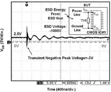
Fig. 4. With a bidirectional-type TVS (part number: P6KE series; breakdown voltages:±6.8 V) between VDDand VSS(ground) of the CMOS IC#1 under
the system-level ESD test, the measured VDDtransient waveform with an ESD
voltage of−1000 V zapping on the HCP. Transient peak voltage on VDDof
CMOS IC#1 can be greatly reduced when it exceeds the VBRof TVS.
With bidirectional-type TVS [part number: P6KE series; breakdown voltages (VBR) :±6.8 V] between VDD and VSS (ground) of the CMOS IC#1 under the system-level ESD test, the measured VDDtransient waveform with an ESD voltage of
−1000 V zapping on the HCP is shown in Fig. 4. With the
equivalent circuit of two Zener diodes in series, but opposite in polarity, TVS can protect CMOS ICs from high-voltage tran-sient surges by shunting the trantran-sient current to have a low clamping voltage across its two terminals. Thus, compared with the original VDDtransient waveform shown in Fig. 2, the ESD-induced voltage on VDDcan be greatly reduced when it exceeds the VBRof the TVS. In addition, both the damping frequency and the damping factor are also different in Fig. 4 because of the parasitic capacitance and inductance in the TVS.
With a resistor-type ferrite bead (minimum impedance of 80 Ω at 25 MHz) in series with the VDD pin of the CMOS IC#1, the measured VDDtransient waveform with an ESD volt-age of−1000 V zapping on the HCP is shown in Fig. 5. With the equivalent circuit of an inductor and a small series resistor, ferrite bead can protect CMOS ICs from the RF field by ab-sorbing the RF energy while the ESD-induced transient current flows through it. Thus, compared with the original VDD tran-sient waveform shown in Fig. 2, there is a smaller trantran-sient peak voltage (larger damping factor) of the VDDtransient waveform in Fig. 5, which has the impacts to the TLU immunity of the CMOS IC#1. From these comprehensive measurements, it has been found that the related dominant parameters of the bipolar trigger voltage to induce TLU, such as transient peak voltage, damping factor, and damping frequency, are strongly dependent on the board-level noise filters.
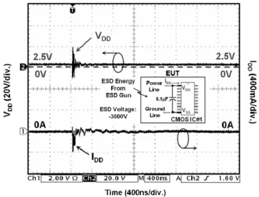
To clarify such a TLU issue, with an ESD voltage of−3000 V zapping on the HCP, the measured VDDand IDDtransient wave-forms on the CMOS IC#1 are shown in Fig. 6. With a large
tran-Fig. 5. With a resistor-type ferrite bead (minimum impedance of 80 Ω at 25 MHz) in series with the VDDpin of the CMOS IC#1 under the system-level
ESD test, the measured VDDtransient waveform with an ESD voltage of−1000
V zapping on the HCP. The transient peak voltage (damping factor) of VDD
waveform is smaller (larger) than that of the original VDDtransient waveform
shown in in Fig. 2.
Fig. 6. Measured VDDand IDDtransient waveforms on the CMOS IC#1 with
an ESD voltage of−3000 V zapping on the HCP. With a large transient peak voltage of±60 V, TLU is triggered on (IDDis kept at a high current of 80 mA)
after the ESD-induced disturbance on VDD.
sient peak voltage of±60 V, a TLU is triggered on with a large transient current of IDD. Thus, IDD is kept at a high current of 80 mA and VDDis pulled down to the latchup holding volt-age of 1.8 V, after the ESD-induced disturbance on VDD. If an additional decoupling capacitance of 0.1 µF is added between
VDD and VSS (ground) of such a TLU-sensitive CMOS IC#1, the measured VDDand IDDtransient waveforms with the same (−3000 V) ESD voltage zapping on the HCP are shown in Fig. 7. Compared with the measured waveforms in Fig. 6, where there is no decoupling capacitance for suppressing the ESD-induced noise, the transient peak voltage (damping factor) of the bipolar trigger waveform is greatly reduced (increased)
Fig. 7. With the decoupling capacitance of 0.1 µF between VDDand VSSof the
CMOS IC#1, the measured VDDand IDDtransient waveforms with the same
(−3000 V) ESD voltage zapping on the HCP. Compared with the measured waveforms shown in Fig. 6, TLU does not occur, because the ESD-induced disturbance on VDDis greatly reduced.
in Fig. 7. As a result, TLU does not occur and IDD does not increase after the ESD-induced disturbance on VDD. Thus, the occurrence of TLU strongly depends on the board-level noise filters, and they should be further investigated to find their im-provements on the TLU immunity of CMOS ICs.
III. TLU MEASUREMENTSETUP
An SCR structure is used as the test structure for TLU mea-surements because the occurrence of latchup results from the parasitic SCR in bulk CMOS ICs. The device cross-sectional view and layout top view of the SCR structure are shown in Fig. 8(a) and (b), respectively. The geometrical parameters D, S, and W represent the distances between well-edge and well (sub-strate) contact, anode and cathode, and the adjacent contacts, respectively. This test structure can simulate the parasitic SCR in real CMOS ICs with the circuit configuration such that the source of PMOS (NMOS) and the N well (P substrate) are con-nected together to VDD(ground). All the SCR structures with different geometrical parameters are fabricated in a 0.25-µm salicided CMOS technology.
During the system-level ESD test, it could be difficult to di-rectly evaluate the TLU immunity of some CMOS ICs inside the EUT. Therefore, a component-level TLU measurement setup with a bipolar trigger waveform was reported [27], as shown in Fig. 9. Such a TLU measurement setup has the advantage of eas-ily evaluating the TLU immunity of a single IC by monitoring the measured voltage/current waveforms through oscilloscope. More importantly, with the ability of generating a bipolar trig-ger voltage, it can accurately simulate how a CMOS IC inside the EUT will be disturbed by ESD-generated noises under the system-level ESD test. In this measurement setup, an ESD sim-ulator is used to generate the bipolar trigger voltage source
VCharge. A capacitor with capacitance of 200 pF used in the machine model (MM) [28] ESD test is employed as the charged
Fig. 8. (a) Device cross-sectional view and (b) layout top view of the SCR structure in the CMOS process for TLU measurements. This test structure can simulate the parasitic SCR in real CMOS ICs.
capacitor. The noise filter network located between the TLU-triggering source and the DUT is used to decouple, bypass, or absorb noise voltage (energy) produced by the TLU-triggering source. The DUT in this work is the SCR structure shown in Fig. 8. The P+ anode and the N+well contact of the SCR are connected together to VDD, whereas the N+ cathode and the P+ substrate contact are connected together to VSS (ground).
IDDis the total current flowing into the P+ anode and the N+ well contact of the SCR. Through an optimal design for plac-ing a small current-limitplac-ing resistance (5 Ω) but removplac-ing the current-blocking diode between the VDD node and the power supply, this measurement setup not only can avoid the pos-sible electrical over-stress (EOS) damage under a high-current latchup state but also can accurately evaluate the TLU immunity of DUT without overestimation [29].
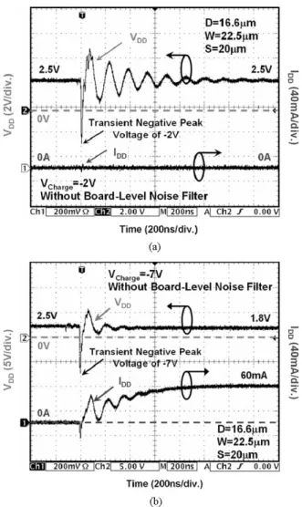
With this component-level TLU measurement setup, the mea-sured VDDand IDDtransient responses with VChargeof−2 and
−7 V are shown in Fig. 10(a) and (b), respectively. The DUT
with an initial VDDbias of 2.5 V is the SCR with specified layout parameters of D = 16.6 µm, S = 20 µm, and W = 22.5 µm.
Fig. 9. Modified component-level TLU measurement setup with bipolar trig-ger [27]. It can accurately simulate how a CMOS IC inside the EUT will be disturbed by the ESD-generated noises under the system-level ESD test.
Fig. 10. Without any board-level noise filters, the measured VDDand IDD
transient responses of the SCR with VChargeof (a)−2 V and (b) −7 V.
No board-level noise filter is added to the DUT during the TLU measurements in Fig. 10(a) and (b). With a smaller VChargeof
−2 V, VDDacts as the intended bipolar trigger voltage just simi-lar to that under the system-level ESD test [30]. In addition, TLU does not occur because IDDdoes not increase after applying the bipolar trigger voltage on VDD, as shown in Fig. 10(a). TLU still
Fig. 11. With an additional decoupling capacitance of 0.1 µF between VDD
and VSS(ground) of the SCR, the measured VDDand IDDtransient responses
with VChargeof−15 V. With the help of the decoupling capacitor for
suppress-ing the transient negative peak voltage of VDDdown to−0.8 V, TLU will not
be initiated.
does not occur until VChargeincreases up to−7 V. Once TLU is initiated, IDDsignificantly increases up to 60 mA, and VDDis pulled down to the latchup holding voltage of 1.8 V, as shown in Fig. 10(b). With an additional decoupling capacitance of 0.1 µF between VDDand VSS(ground) of SCR, the measured VDDand
IDD transient responses with a higher VCharge of −15 V are shown in Fig. 11. With the help of the decoupling capacitor for suppressing the transient negative peak voltage of VDD down to−0.8 V, TLU will not be initiated, even though VCharge is as high as−15 V. As a result, IDDdoes not increase, and VDD is still kept at its normal operating voltage of +2.5 V after ap-plying the bipolar trigger voltage on VDD. From the the TLU measurements in Figs. 10 and 11, this component-level TLU measurement setup can be used to evaluate the effectiveness of the different types of board-level noise filter networks to im-prove the TLU immunity of CMOS ICs under the system-level ESD test.
IV. EXPERIMENTALEVALUATION
Different types of noise filter networks are investigated for their effectiveness to improve the TLU immunity of an SCR structure, including 1) capacitor filter, 2) LC-like filter, 3) π-section filter, 4) ferrite bead, 5) TVS, and 6) hybrid-type filters based on the combinations with TVS and ferrite bead. In this measurement, the SCR structure for all test cases has the same specified layout parameters of D = 16.6 µm, S = 20 µm, and
W = 22.5 µm.
A. TLU Level of the SCR Structure Without Noise Filter Network
Without any noise filter networks, the component-level TLU measurement setup shown in Fig. 9 can be used to evaluate the intrinsic (without noise filter network) TLU level of the SCR with various geometrical parameters. The TLU level is defined as the minimum positive (negative) VChargethat can trigger on
Fig. 12. Measured TLU level of the SCR structures with (a) various D and
W but a fixed S of 1.2 µm and (b) various S and W but a fixed D of 16.6 µm.
The SCR structures are rather susceptible to TLU for all different geometrical parameters (the magnitudes of both positive and negative TLU levels are all smaller than 18 V) unless the SCR is latchup-free.
TLU. Obviously, higher TLU level is better for DUT, because it means that the DUT is less sensitive to TLU under the system-level ESD test. The relations between the TLU system-level and the SCR structures with various geometrical parameters are shown in Fig. 12(a) and (b). The specified SCR structure (with D = 16.6 µm, S = 20 µm, and W = 22.5 µm) used in this work has a very low TLU level [positive (negative) level of +15 V (−7 V)], as shown in Fig. 12(b). Actually, it was found that SCR structures are rather susceptible to TLU for all differ-ent geometrical parameters (the magnitudes of both positive and negative TLU levels are all smaller than 18 V) unless the SCR is latchup-free (i.e., the latchup-holding voltage is larger than the normal operating voltage of +2.5 V). Thus, be-cause of such weak immunity to TLU, the board-level noise filter network is indeed necessary to improve the TLU im-munity of DUT through bypassing, decoupling, or absorbing noise voltage (energy) between the TLU-triggering source and the DUT.
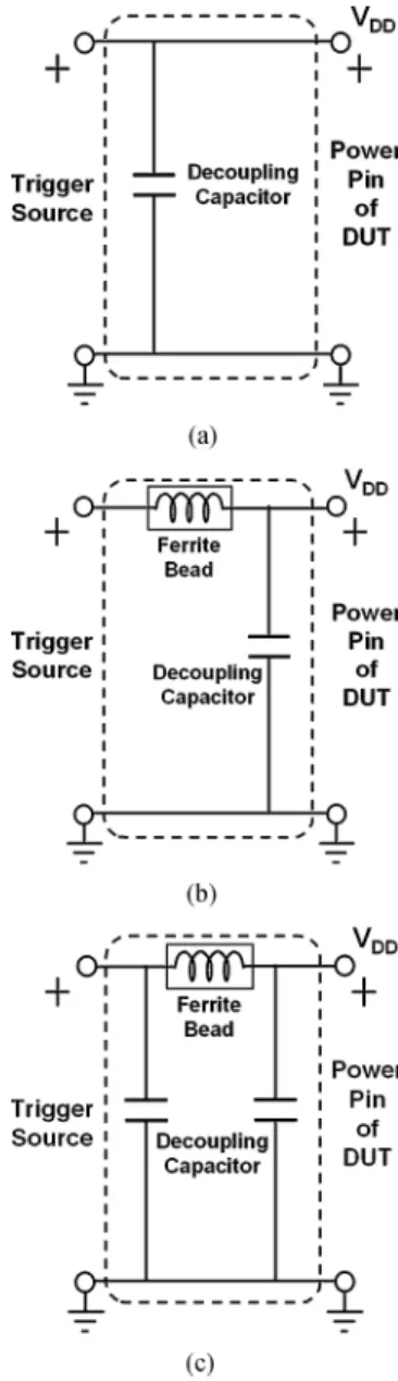
Fig. 13. Three types of noise filter networks investigated for their improve-ments on the TLU level of the SCR. (a) Capacitor filter. (b) LC-like filter. (c) π-section filter.
B. TLU Level of the SCR Structure With Noise Filter Networks 1) Capacitor Filter, LC-Like Filter, and π-Section Filter:
Three types of noise filter networks (capacitor filter, LC-like filter, and π-section filter) are depicted in Fig. 13(a)–(c), respec-tively. Fig. 14 shows their improvements on both positive and negative TLU levels of the SCR structure.
The ceramic disc capacitor with advantages such as high rated working voltage (1 kV), good thermal stability, and low loss at wide range of frequency is employed as the decoupling capac-itor in the noise filter of Fig. 13(a). Decoupling capacitances widely ranging from 100 pF to 0.1 µF are used to investigate their improvements on the TLU level of the SCR structure. With the aid of the capacitor filter to reduce the noise voltage on
VDD, the positive TLU level can be significantly enhanced from +15 V (without decoupling capacitor) to +200 V (with decou-pling capacitance of 0.1 µF), as shown in Fig. 14. Similarly, the negative TLU level can be also greatly enhanced from−7 V
Fig. 14. Relations between the decoupling capacitance and the TLU level of the SCR under three types of noise filter networks: capacitor filter, LC-like filter, and π-section filter.
(without decoupling capacitor) to−160 V (with decoupling ca-pacitance of 0.1 µF). Thus, by choosing a decoupling capacitor with proper capacitance value, a simple first-order decoupling capacitor placed between VDDand VSS(ground) of CMOS ICs can be used to appropriately improve the TLU immunity of the DUT under the system-level ESD test, regardless of the positive or the negative TLU level.
The ferrite bead, which is commonly used for absorbing the RF energy, substitutes for inductor as a second-order LC-like filter component, as shown in Fig. 13(b). Here, a resistor-type ferrite bead [part number: RH 3.5× 9 × 0.8 with minimum impedance of 80 Ω (120 Ω) at 25 MHz (100 MHz)] is em-ployed. Because of a higher insertion loss (second-order fil-ter), such LC-like filter has better TLU level enhancements in comparison with capacitor filter (first-order filter) shown in Fig. 13(a). For example, the positive TLU level can be sig-nificantly enhanced from +15 V (without decoupling capac-itor) to +310 V (with decoupling capacitance of 0.1 µF), as shown in Fig. 14. Similarly, the negative TLU level can be also greatly enhanced from −7 V (without decoupling capacitor) to−280 V (with decoupling capacitance of 0.1 µF). Thus, in order to achieve higher TLU level, the LC-like filter can be used to avoid an excessively or unreasonably large decoupling capacitance in a simple first-order capacitor filter.
A third-order π-section filter is used to further enhance the TLU level of the SCR, as shown in Fig. 13(c). This π-section filter consists of a ferrite bead [the same one shown in Fig. 13(b)] and two decoupling capacitors with equal decoupling capacitance. With the highest insertion loss among the noise fil-ter networks shown in Fig. 13(a)–(c), the TLU level of the SCR can be most greatly improved. For example, the positive TLU level can be significantly enhanced up to +410 V (with decou-pling capacitance of 0.1 µF), as shown in Fig. 14. Similarly, the negative TLU level can be also significantly enhanced up to−370 V (with decoupling capacitance of 0.1 µF). From the comprehensive measured results in Fig. 14, the decoupling ca-pacitance can be optimized according to how large the intended TLU level will be and what kind of board-level noise filter is chosen.
Fig. 15. Four other types of noise filter networks investigated for their im-provements on the TLU level of the SCR. (a) Ferrite bead. (b) TVS. (c) Hybrid type I. (d) Hybrid type II.
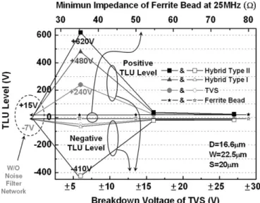
Fig. 16. Relations among the TLU level of SCR, minimum impedance of ferrite bead at 25 MHz, and the breakdown voltage of TVS under four types of noise filter networks: ferrite bead, TVS, hybrid type I, and hybrid type II.
2) Ferrite Bead, TVS, and Hybrid-Type Filters: Four other
types of noise filter networks, ferrite bead, TVS, hybrid type I, and hybrid type II, are depicted in Fig. 15(a)–(d), respectively. Fig. 16 shows their improvements on both positive and negative TLU levels of the SCR structure.
The ferrite bead can absorb the RF energy while the noise-induced transient current flows through it. The resistor-type ferrite beads with three different minimum impedances at 25 MHz are employed in this work: 35, 50, and 80 Ω. However,
a noise filter network with only ferrite bead alone does not perform well enhancement on TLU level because of a worse energy-absorbing ability at frequency lower than 10 MHz [26]. As a result, the TLU level of the SCR structure will not be effi-ciently improved (the magnitudes of both positive and negative TLU levels are all lower than 25 V), even though the minimum impedance of the ferrite bead at 25 MHz is as high as 80 Ω, as shown in Fig. 16.
TVS, which is commonly used to bypass/decouple the high-frequency transient noises, is also considered for its enhance-ment on the TLU immunity of the SCR. The bidirectional-type TVS (part number: P6KE series) with three different breakdown voltages VBR(±6.8, ±16, and ±27 V) are employed. As shown in Fig. 16, the TVS with a breakdown voltage of±16 or ±27 V fails to efficiently improve the TLU level of the SCR (the magnitudes of both positive and negative TLU levels are all lower than 25 V) because TLU occurs prior to the breakdown of such high-VBRTVS. That is, the intrinsic TLU level of the SCR (positive and negative TLU level of +15 and−7 V) is smaller than the VBRof such high-VBRTVS (±16 and ±27 V). Only the TVS with VBRlower than the intrinsic TLU level of the DUT can effectively enhance the TLU level. For example, the positive (negative) TLU level can be enhanced up to +240 V (−50 V) for low-VBR TVS (±6.8 V). Thus, to optimize the efficiency of TVS for TLU prevention, it should be clarified in advance for the correlations between VBRof TVS and the intrinsic TLU level of the DUT.
Hybrid-type filters consisting of both the ferrite bead (mini-mum impedance of 80 Ω at 25 MHz) and the TVS (with different
VBR) are also evaluated for their improvements on the TLU level of the SCR, as shown in Fig. 15(c) and (d). Hybrid types I and II are the counterparts of the LC-like and π-section filters, where the TVS substitutes for the decoupling capacitor as a low-pass filter component. Because the magnitude of an intrinsic TLU level is larger than 7 V, only the hybrid-type filters with a
low-VBRTVS (±6.8 V) can efficiently improve the TLU level, as shown in Fig. 16. For example, hybrid type I with low-VBRTVS (±6.8 V) can greatly enhance the positive (negative) TLU level up to +480 V (−65 V), which is much larger than +25 V (−15 V) for that with high-VBRTVS (±16 and ±27 V). In addition, because such higher-order hybrid type filters provide the higher insertion loss, they can enhance the TLU level of SCR more greatly than ferrite bead or TVS alone. For example, for hybrid type filters with a low-VBR(±6.8 V) TVS, hybrid type I (II) can greatly enhance the positive TLU level up to +480 V (+620 V) and enhance the negative TLU levels up to−65 V (−410 V).
By investigating different types of noise filter networks to find their improvements on TLU levels in Figs. 14 and 16, it can be found that the TVS (hybrid type I) does not improve the negative TLU level as greatly as the first-order capacitor filter (LC-like filter). For example, the negative TLU level can be greatly enhanced up to −160 V (−280 V) for a first-order capacitor filter (LC-like filter) with decoupling capacitance of 0.1 µF, but only up to−50 V (−65 V) for a TVS (hybrid type I) with a low VBRof±6.8 V. Thus, the decoupling capacitor is better than the TVS for being a noise-bypassing component in noise filter networks, because it not only enhances the negative
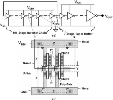
Fig. 17. (a) Schematic diagram and (b) layout top view of the ring oscillator circuit fabricated in a 0.25-µm CMOS process.
TLU level more efficiently, but is also compatible to the CMOS technology for integrating the noise filter into the CMOS chips.
V. VERIFICATION ONREALCIRCUITS
A 100-MHz ring oscillator circuit with 101-stage inverter chain and seven-stage taper buffer fabricated in a 0.25-µm CMOS technology is used as a real circuit to investigate the different types of noise filter networks for their enhancements on TLU levels. The schematic diagram and layout top view of the ring oscillator are shown in Fig. 17(a) and (b), respectively. The geometrical parameters X, Y , and Z in the layout represent the distances between well-edge and well (substrate) contact, source (drain) regions of PMOS and NMOS, and the adjacent well contacts (substrate contacts), respectively. The ring oscil-lator is treated as the DUT in Fig. 9, where the N+well contact and the P+ source of PMOS are connected together to V
DD1, but the P+ substrate contact and the N+source of NMOS are connected to VSS (ground). In addition, the layout parameters of all the taper buffers are fixed, and the power line of the taper buffer (VDD2) with a +2.5 V dc bias is separated from the power line of the inverter chain (VDD1) to evaluate the TLU level of the inverter chain but not the taper buffer. The parasitic SCR structure within the ring oscillator consists of the P+ source of PMOS (anode), N well, P substrate, and the N+ source of NMOS (cathode). In real situation under the system-level ESD test, the TLU can be triggered on by the ESD-generated bipo-lar noise voltage coupled to VDD1of the ring oscillator and so the rapid-increasing current (IDD1) will be conducted through a low-impedance path between VDD1 and ground, eventually probably burning out the chip due to over heating. Thus, the component-level TLU measurement setup shown in Fig. 9 can be used to simulate the system-level ESD test by applying the bipolar trigger voltage on VDD1 and to further evaluate the
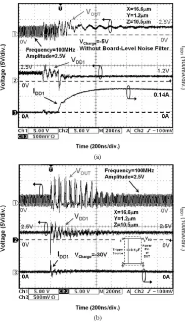
Fig. 18. Measured VDD1, IDD1, and VOUTtransient responses for the ring
oscillator (a) without and (b) with the board-level noise filter network.
effectiveness of the different types of board-level noise filter networks to improve the TLU immunity of the ring oscillator circuit under the system-level ESD test.
To consider the worst case of evaluating the TLU level, the ring oscillator circuit with layout parameters of X = 16.6 µm,
Y = 1.2 µm, and Z = 10.5 µm is used. The anode-to-cathode
spacing (Y ) of 1.2 µm is the minimum allowed distance ac-cording to the foundry design rule. In addition, a large X (Z) of 16.6 µm (10.5 µm) makes sure that there is a large para-sitic well or substrate resistance of the parapara-sitic SCR within ring oscillator, and thus, this ring oscillator circuit has a small latchup triggering current or holding voltage (i.e., most sensitive to latchup).
A. TLU Transient Waveforms of the Ring Oscillator
Fig. 18(a) and (b) shows the measured VDD1, IDD1, and VOUT transient responses for the ring oscillator without and with the
Fig. 19. Relations between the decoupling capacitance and the TLU level of the ring oscillator under three types of noise filter networks: capacitor filter, LC-like filter, and π-section filter.
board-level noise filter network, respectively. For the ring oscil-lator without the board-level noise filter network, the TLU can be triggered on even if the VChargeis as low as−5 V, as shown in Fig. 18(a). Once the TLU is initiated, IDD1will significantly increase (0.14 A) with the pull-down VDD1 (1.2 V) due to a low-impedance latching path between VDD1and ground. Thus, the ring oscillator fails to function correctly, causing the output voltage of the ring oscillator VRingto be pulled down to ground. Therefore, VOUTis kept at +2.5 V after the seven-stage taper buffer.
For the ring oscillator with the board-level noise filter network (capacitor filter with decoupling capacitance of 0.1 µF), TLU does not occur even though the VCharge is as high as −30V, as shown in Fig. 18(b). Clearly, with the aid of the decoupling capacitor to decouple TLU-triggering noises on VDD1, the ring oscillator still maintains its normal function (VOUTwith 100-MHz voltage clock) after the TLU-triggering disturbance on
VDD1.
B. TLU Level of the Ring Oscillator With Noise Filter Networks
Fig. 19 shows the relations between the decoupling capac-itance and the TLU level of the ring oscillator under three types of noise filter networks: capacitor filter, LC-like filter, and π-section filter. With the aid of the first-order capacitor fil-ter (0.1 µF), the positive (negative) TLU level can be enhanced from +8 V (−5 V) to +70 V (−60 V). In addition, higher-order noise filter networks such as LC-like filter and π-section filter can be used to achieve higher TLU level. For example, with a decoupling capacitance of 0.1 µF, the positive (negative) TLU level can be enhanced up to +90 V (−85 V) for the LC-like filter and up to +210 V (−155 V) for the π-section filter.
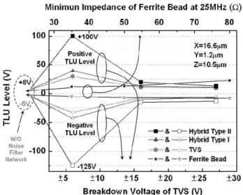
Fig. 20 shows the relations among the TLU level of the ring oscillator circuit, minimum impedance of ferrite bead at 25 MHz, and the breakdown voltage of TVS under four types of noise filter networks: ferrite bead, TVS, hybrid type I, and hybrid type II. Because of the worse energy-absorbing ability of ferrite bead at frequency lower than 10 MHz [26], the TLU level
Fig. 20. Relations among the TLU level of the ring oscillator, minimum impedance of ferrite bead at 25 MHz, and the breakdown voltage of TVS under four types of noise filter networks: ferrite bead, TVS, hybrid type I, and hybrid type II.
will not be efficiently improved by ferrite bead alone (the magni-tudes of both positive and negative TLU levels are all lower than 25 V), even though the minimum impedance of the ferrite bead at 25 MHz is as high as 80 Ω. With the low-VBRTVS (±6.8 V) alone, the positive (negative) TLU level can be enhanced up to +30 V (−33 V). Such low-VBRTVS can be used in hybrid-type filters to further enhance the TLU level. As shown in Fig. 20, the positive (negative) TLU level is only +30 V (−33 V) for TVS alone, but it can be enhanced up to +40 V (−42 V) for hybrid type I and up to +100 V (−125 V) for hybrid type II.
Among the comprehensive measured results in Figs. 14, 16, 19, and 20, through investigating the TLU level enhancements by different types of noise filter networks for standalone SCR and the ring oscillator circuit, the TLU levels of the ring os-cillator are overall smaller than those of the SCR. The reason for this is that the ring oscillator has smaller dc latchup trigger current (voltage) due to both the layout geometrical parameters and the larger total p-n junction area. That is, the ring oscilla-tor circuit is more sensitive to latchup than is the SCR. Thus, the effectiveness of noise filter networks to enhance the TLU immunity strongly depends on the DUT. As a result, the dc latchup characteristics of the DUT should be identified in ad-vance when board-level noise filter networks are designed to improve the TLU immunity of the DUT under the system-level ESD test.
VI. CONCLUSION
By choosing proper components in each noise filter network, the TLU immunity of CMOS ICs under the system-level ESD test can be greatly improved. From the experimental results it has been found that the decoupling capacitor is better than the TVS for being a noise-bypassing component in the noise filter networks because it not only enhances the negative TLU level more efficiently but is also compatible to the CMOS technology for integrating the noise filter into chips. In addition, the TLU
level enhancements by different types of noise filter networks strongly depend on the DUT. Thus, the dc latchup characteristics of the DUT should be identified in advance when the board-level noise filter networks are designed to improve the TLU immunity of the DUT under the system-level ESD test. The optimal design for enhancements of the TLU immunity can be achieved through well characterization between the intrinsic latchup characteristics of the DUT as well as the efficiency of TLU prevention from different kinds of board-level noise filters. To further improve the TLU immunity of electronic products, chip-level solutions should be adopted along with board-level solutions to meet the applications with high system-level ESD specification.
ACKNOWLEDGMENT
The authors would like to thank Dr. C.-C. Tasi, Dr. T.-Y. Chen, and Mr. W.-Y. Lo for their valuable technical discussions.
REFERENCES
[1] D. B. Estreich, A. Ochoa, Jr., and R. W. Dutton, “An analysis of latch-up prevention in CMOS IC’s using an epitaxial-buried layer process,” in
IEDM Tech. Dig., 1978, pp. 230–234.
[2] R. R. Troutman, “Epitaxial layer enhancement of n-well guard rings for CMOS circuits,” IEEE Electron Device Lett., vol. 4, no. 12, pp. 438–440, Dec. 1983.
[3] R. R. Troutman and H. P. Zappe, “A transient analysis of latchup in bulk CMOS,” IEEE Trans. Electron Devices, vol. 30, no. 2, pp. 170–179, Feb. 1983.
[4] E. Hamdy and A. Mohsen, “Characterization and modeling of transient latchup in CMOS technology,” in IEDM Tech. Dig., 1983, pp. 172–175. [5] R. R. Troutman and H. P. Zappe, “Layout and bias considerations for
preventing transiently triggered latchup in CMOS,” IEEE Trans. Electron
Devices, vol. ED-31, no. 3, pp. 315–321, Mar. 1984.
[6] R. R. Troutman, Latchup in CMOS Technology: The Problem and the
Cure. New York: Kluwer, 1986.
[7] W. Morris, “Latchup in CMOS,” in Proc. IRPS, 2003, pp. 76–84. [8] S. Voldman, E. Gebreselasic, L. Lanzerotti, T. Larsen, N. Feilchenfeld,
S. St. Onge, A. Joseph, and J. Dunn, “The influence of a silicon dioxide-filled trench isolation structure and implanted sub-collector on latchup robustness,” in Proc. IRPS, 2005, pp. 112–120.
[9] S. Voldman, E. Gebreselasic, M. Zierak, D. Hershberger, D. Collins, N. Feilchenfeld, S. St. Onge, and J. Dunn, “Latchup in merged triple well structure,” in Proc. IRPS, 2005, pp. 129–136.
[10] C. Duvvury and G. Boselli, “ESD and latch-up reliability for nanometer CMOS technologies,” in IEDM Tech. Dig., 2004, pp. 933–936. [11] G. Boselli, V. Reddy, and C. Duvvury, “Latch-up in 65 nm CMOS
tech-nology: A scaling perspective,” in Proc. IRPS, 2005, pp. 137–144. [12] S. Voldman, “Latchup and the domino effect,” in Proc. IRPS, 2005,
pp. 145–156.
[13] , “Latch-up—It’s back,” Threshold Newslet., Sep./Oct. 2003. [14] S. Bargst¨atd-Franke, W. Stadler, K. Esmark, M. Streibl, K. Domanski,
H. Gieser, H. Wolf, and W. Bala, “Transient latch-up: Experimental anal-ysis and device simulation,” in Proc. EOS/ESD Symp., 2003, pp. 70–78. [15] J. T. Mechler, C. Brennan, J. Massucco, R. Rossi, and L. Wissel,
“Contention-induced latchup,” in Proc. IRPS, 2004, pp. 126–129. [16] K. Domanski, S. Bargst¨adt-Franke, W. Stadler, M. Streibl, G. Steckert, and
W. Bala, “Transient-LU failure analysis of the ICs, methods of investiga-tion and computer aided simulainvestiga-tions,” in Proc. IRPS, 2004, pp. 370–374. [17] K. Domanski, S. Bargst¨atd-Franke, W. Stadler, U. Glaser, and W. Bala, “Development strategy for TLU-robust products,” in Proc. EOS/ESD
Symp., 2004, pp. 299–307.
[18] K. Chatty, P. Cottrell, R. Gauthier, M. Muhammad, F. Stellari, A. Weger, P. Song, and M. McManus, “Model-based guidelines to suppress cable discharge event (CDE) induced latchup in CMOS ICs,” in Proc. IRPS, 2004, pp. 130–134.
[19] C. J. Brennan, K. Chatty, J. Sloan, P. Dunn, M. Muhammad, and R. Gauthier, “Design automation to suppress cable discharge event (CDE)
Measurements, and Technologies. Piscataway, NJ: IEEE Press, 1996. [26] M. I. Montrose, Printed Circuit Board Design Techniques for EMC
Com-pliance. Piscataway, NJ: IEEE Press, 2000.
[27] I. Morgan, C. Hatchard, and M. Mahanpour, “Transient latch-up using an improved bi-polar trigger,” in Proc. EOS/ESD Symp., 1999, pp. 190–202. [28] Electrostatic Discharge (ESD) Sensitivity Testing—Machine Model (MM),
EIA/JEDEC Standard Test Method A115-A, 1997.
[29] M.-D. Ker and S.-F. Hsu, “Evaluation on efficient measurement setup for transient-induced latchup with bi-polar trigger,” in Proc. IRPS, 2005, pp. 121–128.
[30] M.-D. Ker and Y.-Y. Sung, “Hardware/firmware co-design in an 8-bits microcontroller to solve the system-level ESD issue on keyboard,” in
Proc. EOS/ESD Symp., 1999, pp. 352–360.
Ming-Dou Ker (S’92–M’94–SM’97) received the
B.S., M.S., and Ph.D. degrees from the National Chiao-Tung University, Hsinchu, Taiwan, R.O.C., in 1986, 1988, and 1993, respectively.
In 1994, he joined the VLSI Design Department of the Computer and Communication Research Lab-oratories (CCL), Industrial Technology Research In-stitute (ITRI), Taiwan, as a Circuit Design Engineer. In 1998, he was the Department Manager in the VLSI Design Division of CCL/ITRI. He is now a Full Pro-fessor at the National Chiao-Tung University. He has published over 250 technical papers in international journals and conferences in
committee for the 2005 IEEE International Reliability and Physics Symposium (IRPS), and the Chair of TRD track of the 2006 IEEE International Symposium on Quality Electronic Design (ISQED). He also served as the Technical Program Committee Chair of 2002 Taiwan ESD Conference, the General Chair of the 2003 Taiwan ESD Conference, the Publication Chair of 2004 IPFA, and the ESD Program Chair of the 2004 International Conference on Electromagnetic Appli-cations and Compatibility. He was the Organizer of the Special Session on ESD Protection Design for Nanoelectronics and Gigascale Systems in ISCAS 2005. He has also served as the Associate Editor of the IEEE TRANSACTIONS ONVLSI SYSTEMS. He was elected as the President of the Taiwan ESD Association in 2001. He has received many research awards from ITRI, National Science Coun-cil, and National Chiao-Tung University and the Dragon Thesis Award from the Acer Foundation. In 2003, he was selected as one of the Ten Outstanding Young Persons in Taiwan by Junior Chamber International (JCI). In 2005, one of his patents on ESD ptotection design received the National Invention Award in Taiwan.
Sheng-Fu Hsu (S’04) received the B.S. degree from
the National Tsing-Hua University, Hsinchu, Taiwan, R.O.C. in 2000 and the M.S. degree from the National Chiao-Tung University, Hsinchu, in 2002. He is cur-rently pursuing the Ph.D. degree from the National Chiao-Tung University.
His current research interests include semiconduc-tor device physics and IC reliability.