chip module (MCM) for low phase-noise (PN) -band frequency generation. A high-performance 8 GaAs metamorphic high-elec-tron mobility transistor monolithic microwave integrated circuit (MMIC) multiplier and a low PN 7-GHz GaAs InGaP hetero-junction bipolar transistor (HBT) MMIC oscillator were used in the module. The microstrip MMICs were FC bonded to an Al2O3 carrier with patterns optimized for low-loss transitions. The FC-based module was experimentally characterized to have a PN of 88 dBc/Hz @ 100-kHz offset and 112 dBc/Hz @ 1-MHz offset with an output power of 11 dBm. For compar-ison, the MMICs were also FC bonded as individual chips and the performance was compared with the bare dies without FC bonding. It was verified that the FC bonding has no detrimental effect on the MMIC performance. The tests revealed that the FC module provided improved performance. To our best knowledge, this is the first FC-based module for millimeter-wave frequency generation. The module also presents one of the best PN reported for millimeter-wave frequency sources.
Index Terms—Flip-chip (FC), frequency generation, intercon-nection, millimeter wave, monolithic microwave integrated circuit (MMIC), multichip module (MCM), multiplier, oscillator, phase noise (PN), -band.
Manuscript received July 27, 2009; revised May 10, 2010; accepted June 16, 2010. Date of publication August 03, 2010; date of current version September 10, 2010. This work was supported by the Swedish Agency of Innovation Sys-tems (VINNOVA), Chalmers University of Technology, Ericsson AB, Sivers IMA AB, Krisberedskapsmyndigheten (KBM), Försvarets materielverk (FMV), and by the National Science Council of Taiwan and Ministry of Economic Af-fairs, Taiwan under Contract NSC 96-2752-E-009-001-PAE and Contract NSC 95-EC-17-A-05-S1-020.
L.-H. Hsu is with the Department of Materials Science and Engineering, National Chiao Tung University, Hsinchu 300, Taiwan, and also with the Microwave Electronics Laboratory, Department of Microtechnology and Nanoscience, MC2, Chalmers University of Technology, Göteborg SE-412 96, Sweden (e-mail: [email protected]; [email protected]).
D. Kuylenstierna, R. Kozhuharov, and H. Zirath are with the Gigahertz Centre, Microwave Electronics Laboratory, Department of Microtechnology and Nanoscience, MC2, Chalmers University of Technology, Göteborg SE-412 96, Sweden (e-mail: [email protected]; [email protected]; [email protected]).
M. Gavell is with the the Microwave Electronics Laboratory, Chalmers University of Technology, Göteborg SE-412 96, Sweden (e-mail: marcus. [email protected]).
C. Kärnfelt was with the Gigahertz Centre, Microwave Electronics Labora-tory, Chalmers University of Technology, Göteborg SE-412 96, Sweden. She is now with the Microwave Départment, Télécom Bretagne, Brest CS 83818, France (e-mail: [email protected]).
W.-C. Lim and E. Y. Chang are with the Department of Materials Science and Engineering, National Chiao Tung University, Hsinchu 300, Taiwan (e-mail: [email protected]).
Color versions of one or more of the figures in this paper are available online at http://ieeexplore.ieee.org.
Digital Object Identifier 10.1109/TMTT.2010.2057135
L
OW phase-noise (PN) millimeter-wave frequency genera-tion is a critical issue for future multigigabit/second wire-less communication systems. The millimeter-wave frequency bands are capable of carrying high data rates thanks to the large amount of bandwidth available, e.g., the license-free industrial, scientific, and medical (ISM) bands around 60 GHz [1], or the recently allocated -band (71–76 and 81–86 GHz) [2]. Further increased data rates may be reached with spectral efficient mod-ulation formats, e.g., higher order quadrature amplitude modu-lation (QAM) [2]. However, the spectral-efficient modumodu-lation also puts stringent requirements on signal purity, i.e., low PN, which is challenging at millimeter-wave frequencies. One so-lution could be to operate the local oscillator (LO) at a lower frequency and use frequency multipliers [3] to reach the target frequency. It is believed that the overall PN will be lower with this approach as the factor of the resonant tank in the oscillator is reduced with increased frequency [4]. The use of frequency multipliers to create millimeter-wave signals also decrease or even totally diminish the need of frequency dividers for phase locking.Although it is possible to design single-chip solutions where the oscillator and multiplier are integrated on the same monolithic microwave integrated circuit (MMIC), it may be advantageous to address a multichip module (MCM) [5]–[7] approach enabling higher flexibility in choice of technology for each chip. However, MCM packaging at millimeter-wave frequencies is also challenging, the interconnections between the MMIC chips and the MCM carrier may decay the assembly performance, e.g., conventional bond-wires give a significant contribution to the parasitic inductance, and thus, induce unwanted effects at millimeter-wave frequencies [8]. In this respect, flip-chip (FC) interconnection has been regarded as a promising packaging technology for cost-effective module assembly in millimeter-wave systems due to its shorter inter-connect length, higher throughput, and smaller package size [9]–[16]. Furthermore, considering large-scale production with small chip ( 5 5 mm ) and pad ( 1 1 mm ) size and good wafer-bumping yield, the FC is cheaper than bond-wire [16]. For millimeter-wave applications, the regular chip and pad size is normally smaller than this range. For these reasons, the FC-based multichip module (FC-MCM) is considered as the most promising packaging scheme for millimeter-wave wireless applications.
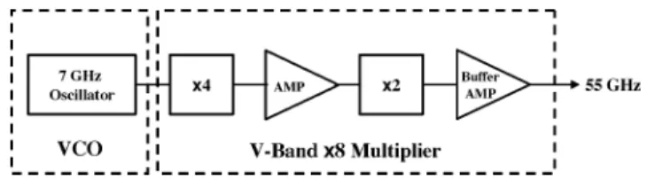
Fig. 1. Block diagram of theV -band frequency source realized in this study.
Fig. 2. Simulated FC interconnect structure (single transition).
In this paper, we report on an FC-MCM for -band fre-quency generation. Fig. 1 illustrates the block diagram of the -band frequency source realized in this study. The module consists of the high-performance -band 8 metamorphic high-electron mobility transistor (mHEMT) MMIC multiplier reported in [3] and the 7-GHz low PN cross-coupled InGaP HBT MMIC oscillator reported in [17]. This paper is organized as follows. In Section II, the optimum FC design by electro-magnetic (EM) simulation will be presented and discussed. In Section III, the in-house process flow of FC assembly will be presented. Sections IV and V present the measurement setups and measurement results for the MMIC circuits, respectively. Finally, this work is concluded in Section VI.
II. DESIGN ANDOPTIMIZATION OF THEFC TRANSITIONS
In this work, the oscillator and 8 multiplier MMICs were designed with microstrip (MS) transmission lines as most of the commercial available MMICs. However, most of the re-ported FC studies have been made using coplanar waveguide (CPW) MMICs [9]–[14], which is considered to be more com-patible with FC technology. Hence, the FC structure design for MS MMICs needs to be investigated. The design and optimiza-tion of the interconnect structure was carried out by using the simulation tool, Ansoft High Frequency Simulation Software (HFSS) 11 for the 3-D EM field analysis, which predicts a reli-able -parameter of the millimeter-wave interconnect structures [18]–[20]. Fig. 2 shows the simulated FC interconnect structure with the MS transmission line on the GaAs chip and CPW trans-mission line on the Al O carrier.
The important parameters of the FC design such as bump di-ameter, bump height, metal pad overlap, and compensation have been discussed and investigated in [9], [11], and [12]. Among these parameters, the compensation, reducing the excess para-sitic capacitance at the vertical bump transition by adding an
Fig. 3. Illustrations of the important parameters for the FC interconnect.
inductive counterpart, is the most effective way to optimize the interconnect performances since extra process steps and fabri-cation cost are not needed [11]. Two approaches, one with stag-gered bumps and the other one employs a high impedance-line section, were proposed to reduce the return loss of the FC inter-connect [9], [11]. The staggered-bumps approach needs an ad-ditional chip area and requires customized chip design. There-fore, the approach of employing a high-impedance line section before the bump transitions is more advantageous.
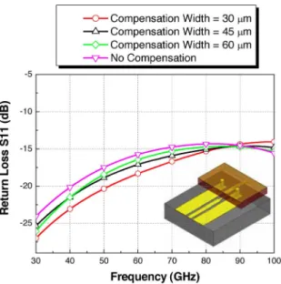
During the EM simulation, the bump dimensions and metal pad overlap were fixed by the fabrication process. The diam-eter of the bump was 50 m, the bump height was 40 m, and the metal pad overlap was 70 m. The center-to-center distance between signal and ground bumps was 150 m. The illustra-tions of these parameters are indicated in Fig. 3. Figs. 4 and 5 show the simulated return loss ( ) and insertion loss ( ), respectively, of the FC interconnect with different compensa-tion widths. As can be seen, the thinner the high-impedance line compensation, the better the interconnect performance. From Fig. 4, the return loss was improved about 3 dB per transi-tion at 60 GHz compared to the structure without compensa-tion. Besides, the insertion loss was about 0.5 dB per transi-tion at 60 GHz after optimizatransi-tion (Fig. 5). The final dimensions of the compensation line were 30 m in width and 50 m in length, which is acceptable for commercial low-cost film mask processes. Table I shows the parameters of the optimized FC de-sign.
III. FABRICATION OF THEFC-BASEDMODULES
One of the advantages with MCMs compared to highly in-tegrated single chips is the flexibility to adapt technology for the individual chip functions; in a single-chip solution, the tech-nology is a tradeoff between the different chip functions. The -band LO module reported in this work is assembled from a low-PN 7-GHz fixed-frequency cross-coupled oscillator de-signed and implemented in a GaAs InGaP HBT [17] process and a 8 GaAs mHEMT multiplier chain optimized for input fre-quency in the range of 6.5–8 GHz [3]. The InGaP HBT process
Fig. 4. Simulated return loss (S11) of the FC interconnect (single transition) with different compensation widths.
Fig. 5. Simulated insertion loss (S21) of the FC interconnect (single transition) with different compensation widths.
TABLE I
PARAMETERS OF THEOPTIMIZEDFC DESIGN
is an excellent choice for low PN oscillators thanks to the good low-frequency noise properties and the high breakdown voltage
Fig. 6. Process flow of the Al O carrier for FC assembly.
[4]. The cross-coupled topology is chosen for its relatively good PN properties and ease of startup [21]. To simplify the bias scheme, a fixed-frequency oscillator is used instead of a voltage-controlled oscillator (VCO) as the major goal is to demonstrate the concept of building practice providing a low PN at -band.
A. Process Technology for the Al O Carrier
The Al O carrier used for FC assembly of the MMICs was in-house fabricated in the Compound Semiconductor Laboratory (CSDLab), National Chiao Tung University (NCTU), Hsinchu, Taiwan [15]. Alumina (Al O ) was chosen as the packaging carrier because of its good electrical char-acteristics for high-frequency applications ( and ). Moreover, Al O has a thermal expansion coefficient ( ppm/ C) very close to that of GaAs ( ppm/ C), which can minimize potential thermal stress between the MMICs and the carrier, e.g., caused by temperature variations. The thickness of the Al O carrier used in this study is about 254 m (10 mil). Fig. 6 shows the process flow of the Al O carrier used for FC assemblies. Gold (Au) metal, formed by cyanide-based electroplating, was used as the metallization of the transmission line and the vertical transition bumps. Firstly, Ti and gold metal were in-situ deposited using an E-gun evaporator onto the Al O carrier with the thickness of 300 and 500 Å to form a continuous seed layers for gold electroplating. Ti was used as an adhesion layer. A thin photoresist (PR) was then patterned on the carrier for electroplating of the CPW circuits. After the electroplating of the gold circuits, the thin PR was removed. The wafer was then covered by a thick PR patterned to define the positions of the gold bumps that were formed by electroplating. By controlling the electroplating current density and time, the required bump height was achieved. The gold-bump height and diameter in this study were 40 and 50 m, respectively. The seed layers were then removed with a KI/I solution for the removal of
Fig. 7. (a) Cross-sectional SEM image of the thick PR profile before gold bump electroplating. (b) SEM image of the electroplated gold circuits and bumps on the Al O carrier.
gold metal and HF dilute solution for the removal of the Ti metal. Fig. 7 shows the scanning electron microscope (SEM) image of the thick PR profile and the electroplated gold circuits and bumps on the Al O carrier.
B. Chip Assembly Process
The MMIC oscillator and the 8 multiplier chips were FC bonded onto the Al O carrier by the Au-to-Au thermo-com-pression method using a PP-5 TSV assembly machine from JFP Microtechnic, Marcoussis, France. After optimization, the tem-perature of the work holder was set to 300 C and the bonding force was adjusted to 20 grams per bump, which was main-tained for a bonding time of 60 s. As reference to the FC bonded module, the oscillator and multiplier were also attached using silver epoxy on a piece of brass and connected with conven-tional bond-wire technology. For further comparison, the indi-vidual oscillator and multiplier MMICs were also FC bonded and compared with the bare chip performances.
IV. CIRCUITCHARACTERIZATION
All the measurements were performed in the Microwave Electronics Laboratory (MEL), Department of Microtech-nology and Nanoscience (MC2), Chalmers University of Technology, Göteborg, Sweden. The output power, oscillation frequency, and PN of the oscillators were measured using an HP8565EC spectrum analyzer. For characterization of the 8 multiplier, an HP83650B frequency synthesizer was used as the input signal source and the HP8565EC spectrum analyzer com-plemented with HP11974V -band external mixers was used for measuring output power, PN, and oscillation frequency. -parameter measurements of the 8 multiplier were also carried out using an Agilent precision network analyzer (PNA) E8361A. For comparison, the MMIC chips were measured before and after FC assembly.
The FC mounted -band LO modules were characterized using the same spectrum analyzer and mixers as used for the
8 multiplier.
V. MEASUREMENTRESULTS ANDDISCUSSIONS
A. 7-GHz Cross-Coupled HBT Oscillators
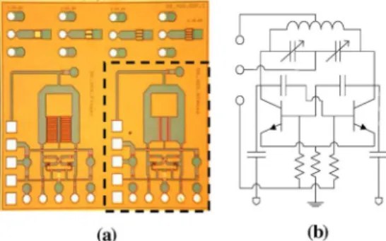
Fig. 8 shows the chip photograph and circuit schematic of the cross-coupled HBT oscillator. There are two circuits in the same chip. The circuit on the right side is the fixed-frequency oscil-lator used in this study. Since the two circuits were not
sepa-Fig. 8. (a) Chip photograph (right-hand side) and (b) circuit schematic of the cross-coupled HBT oscillator.
Fig. 9. Photograph of the FC bonded HBT oscillator.
Fig. 10. Cross-sectional view of the simulated resonant tank of the oscillator taking the FC effect into account.
rated by dicing, the circuit on the left side was used as addi-tional support by designing dummy bumps underneath its pads. The total chip area is 1.8 2 mm . Fig. 9 shows the photo-graph of the FC bonded HBT oscillator. To investigate the in-fluence of the FC mounting, an EM simulation was carried out in ADS Momentum. Fig. 10 shows a cross-sectional view of the simulated resonant tank of the oscillator with the effect from the FC carrier taken into account. A 40- m-thick layer of air layer and a 254- m-thick Al O layer were added to represent the FC carrier in the Momentum substrate definition. Fig. 11 shows the simulated phase of the input impedance versus frequency before and after FC assembly. From the phase-fre-quency curve in Fig. 11, the factor can be calculated as
(1)
The calculated factors before and after the FC are estimated to be 28 and 33, respectively, i.e., 18% improvement in factor
Fig. 11. Simulated phase of the input impedance (Z ) of the oscillator versus frequency before and after FC assembly.
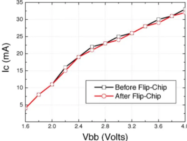
Fig. 12. Measured collector current of the oscillator before and after FC as-sembly. The collector bias voltage isV cc = 8 V.
of the resonant tank after FC assembly. In both cases, the res-onant-frequency was 7.2 GHz, the shift in resonant frequency due to Al O is negligible.
As seen in Fig. 8, the cross-coupled oscillator has a balanced output. The characterization of the circuit was accomplished by measuring one of the outputs, while the other was terminated in a 50- load. Both outputs were also externally attenuated 3 dB to reduce the loading of the oscillator. Fig. 12 shows the mea-sured dc current consumption of the oscillator, i.e., versus at V, before and after FC assembly. After the FC, the current consumption was lower. Although the reduction was marginally within the range of the measurement accuracy, a slight reduction could be expected due to the improved tank . Fig. 13 shows the measured output power and oscillation frequency versus base voltage ( ). After FC assembly, the output power remained the same and the oscillation frequency was shifted as little as 25 MHz (0.35%).
To predict the oscillator PN, the -parameters from the Mo-mentum simulation were inserted into the oscillator equivalent circuit and the PN simulated with the harmonic balance tool in Agilent Technologies Advanced Design System (ADS). Fig. 14 shows measured and simulated PN for the flip-chipped oscillator and the probed MMIC oscillator compared to simulations. As
Fig. 13. Measured output power and frequency of the oscillator as function of the base voltage (V bb) before and after FC.
Fig. 14. Measured and simulated PN of the oscillator before and after FC as-sembly. The collector bias voltage isV cc = 8 V.
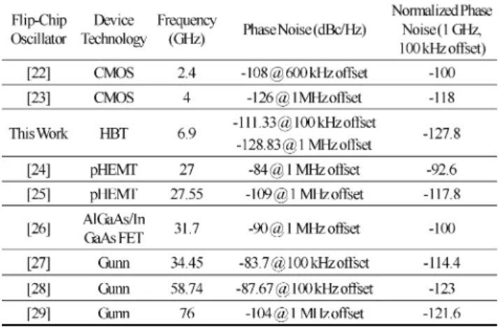
can be seen in Fig. 14, the PN was improved after FC assembly, probably due to the better factor resulting from the mounting effect of the FC. The simulation and measurement results cor-respond well below V. Above V, the sim-ulated results do not agree with the measurements, the reduced PN in simulation is most likely an artifact from model limita-tions when the oscillator goes into the voltage limited region. After FC assembly, the lowest PN are 112 dBc/Hz @ 100-kHz offset and 128 dBc/Hz @ 1-MHz offset. Compared to the pre-vious publications [22]–[29], this is the lowest PN reported for an FC assembled oscillator. Table II presents the key figures of the FC oscillator in this work compared to FC oscillators in the open literature. To be able to compare PN of oscillators oper-ating at different frequencies, the results are bench-marked after a normalized PN at 1-GHz and 100-kHz offset, cal-culated using Leeson’s equation [30]
TABLE II
FC OSCILLATOR INTHISWORKCOMPARED TO FC OSCILLATORS INOPENLITERATURE
where is the oscillation frequency in gigahertz and is PN measured at an offset frequency (in kilohertz). The figure-of-merit (FOM) resembles the conventional os-cillator FOM [30] apart from the fact that it does not include the power consumption, which is intentionally omitted as it mixes up two parameters into the same FOM. The dc power consump-tion of the oscillator in this work is (in milliwatts), which would yield a FOM of 187 using the defi-nition in [31], which is very competitive. However, it is better to present PN and power consumption individually. The require-ments on PN must first be fulfilled. It must then be verified that the power consumption is not too high for the application in mind.
Despite normalization in terms of oscillation and offset fre-quency, the comparison in Table II has limitations, e.g., it does not differ between fixed-frequency oscillators and VCOs. It is reasonable to question whether the good result is reached for our FC demonstrator (see Table II), thanks to the fact of using a fixed-frequency oscillator instead of a MMIC VCO. Most likely, a similar demonstrator based on a VCO would have about 6–8-dB higher PN, the difference between a MMIC oscillator and a VCO [17]. In this regard, our demonstrator would still be well placed in the comparison, none of the VCOs in Table II achieves PN better than this range. Another interesting aspect worth mentioning in the discussion of Table II is that most of the cited works are using high- passives on the FC motherboard, while this work demonstrates the FC of a bare-die MMIC oscil-lator so it is easy to see that FC assembly does not degrade the PN (see Fig. 14).
It should be mentioned that data compared in this work are measured with the HP8565EC spectrum analyzer, the MMIC oscillator was also measured using a dedicated PN measure-ment system Agilent 5500A with better noise floor. A PN as low as 117 dBc/Hz at 100 kHz off-set was then reached [17]. However, the Agilent 5500A system cannot be used at -band frequencies. For this reason, we refer to the result from the spec-trum analyzer in order to have a fair comparison to the -band measurements.
B. -Band 8 mHEMT Multiplier
Fig. 15 shows the circuit schematic of the mHEMT multiplier by eight ( 8). It includes an input matching common-gate stage followed by a quadruper ( 4), a feedback amplifier, a doubler ( 2), and a buffer amplifier at the output. The topology was chosen for realization of a highly integrated -band LO chain with high output power and good harmonic suppression. The input matching and interstage amplification were designed to occupy minimum chip area [3]. For measurements, the
ampli-fiers were biased at V and V; the
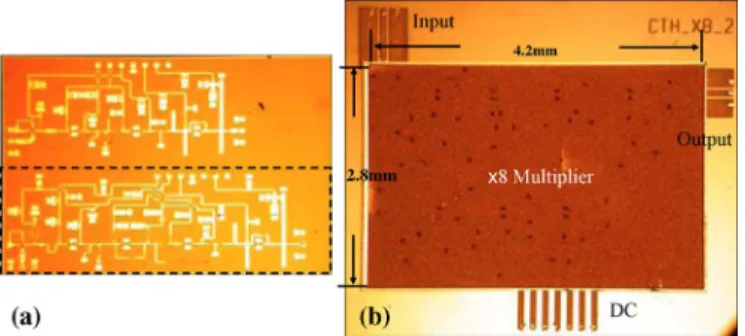
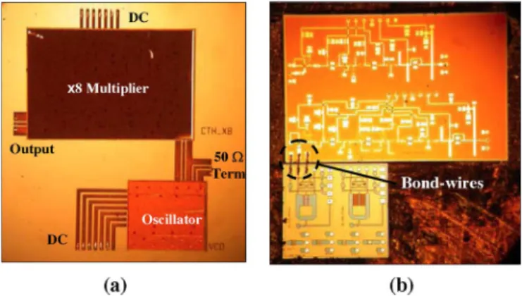
quadrupler and doubler were biased at V and V. Fig. 16 shows a photograph of the 8 multi-plier before and after FC assembly. As can be seen, the lower circuit is the 8 multiplier used in this study. Since the circuits were not separated by dicing, the upper circuit (useless part) was used as additional support by designing dummy bumps under-neath its pads. The total chip area is 2.8 4.2 mm .
To investigate the input and output matching of the multiplier, the -parameter of the 8 multiplier was measured and com-pared before and after FC assembly. As can be seen in Fig. 17, in the frequency range of 7–12 GHz, the input matching is better than 15 dB, which is an improvement compared to the data before the FC. Similarly, the output return loss was im-proved 5–10 dB (from 53 to 67 GHz) after FC assembly (see Fig. 18). The significant improvement is due to the flipping onto the CPW line, which ameliorates the matching to probes a lot at higher frequencies. In our later designs, the output RF pads on the chip were simulated, optimized, and modified to a short part of the CPW with a couple of via-holes to each ground plane (for frequencies higher than 50 GHz). There are many publica-tions dedicated to a similar mollified RF pad. In conclusion, we would define the improvement as a consequence of connection to the CPW and the improvement according to the graph, which demonstrates the influence of compensation at high frequencies. After the -parameter measurements, the output power char-acteristics as function of input power and frequency were inves-tigated. Fig. 19 presents the comparison of the measured output power versus input power before and after FC assembly. The input frequency was set at 7 GHz instead of 8.1 GHz, where the best was obtained according to Fig. 17. The reason for using 7 GHz is that it is the oscillation frequency of the cross-coupled HBT oscillator that is connected to the input of the 8 multiplier in the -band MCM frequency source. Fig. 19 shows that the output power was essentially unaffected by FC assembly. Only a small shift in the saturation point was detected. After the FC, the saturation occurs at lower input power, probably due to better input and output matching. Under variation of the input fre-quency with constant input power dBm (see Fig. 20), the peak-output power shifted to lower frequency (from 56 to 54 GHz). An increased bandwidth was also observed, as ex-pected, which is due to the improvement in the output matching (Fig. 18).
C. FC-Based -Band MCM Frequency Source
It is now demonstrated that the FC does not have any signifi-cant negative effect on either the cross-coupled oscillator MMIC or the 8 multiplier MMIC. The next step is to combine the two into one FC MCM frequency source with hybrid device
Fig. 15. Circuit schematic of the28 mHEMT MMIC multiplier.
Fig. 16. Photographs of the28 mHEMT MMIC multiplier (a) before and (b) after FC assembly.
Fig. 17. Measured input return lossS11 of the 28 multiplier before and after FC assembly.
technology on the Al O carrier. Meanwhile, a bond-wire con-nected module was also realized for comparison. Fig. 21 shows the photographs of the FC and bond-wire assembled -band LO MCMs. For the FC scheme, there are three transitions in the module, which are: 1) oscillator output to CPW on Al O (7 GHz); 2) CPW on Al O to 8 input (7 GHz); and 3) 8 output to CPW on Al O (55 GHz). For the bond-wire scheme, the measurements were carried out by probing directly on the MMIC circuits, which means that there is only one bond-wire transition from the oscillator output to the 8 input (7 GHz) in the module. In Fig. 13, the output power of the oscillator is around 7 dBm. Moreover, the loss from the oscillator output to the 8 input at 7 GHz can almost be ignored for both FC and bond-wire schemes since the output power of the oscillator is
Fig. 18. Measured output return lossS22 of the 28 multiplier before and after FC assembly.
Fig. 19. Measured output power of the28 multiplier versus input power before and after FC assembly (Input frequency= 7 GHz).
6 dBm and the loss of about 1 dB due to the chip-to-chip trans-mission still keeps the 8 in compression at 0 dBm, as shown in Fig. 19. The bond-wire version, as a result, was expected to have higher output power at the 8 output because, in this case, the transition from the MMIC to Al O carrier was not in-cluded in the measurement. Fig. 22 presents a comparison of the measured output power and oscillation frequency versus oscil-lator base-voltage ( ) of the FC and bond-wire assembled LO MCMs. As indicated in Fig. 21(a), the carrier for the FC-based module is prepared for the termination of the nonused output.
Fig. 20. Measured output power of the28 multiplier versus frequency before and after FC assembly (Input power= 0 dBm).
Fig. 21. Photograph of the: (a) FC and (b) bond-wire assembledV -band LO MCM module.
In principle, this output could be connected to a phase-locked loop (PLL) for phase locking. However, in the measurements, it was terminated in a 50- load preceded by 3-dB attenuation. For the bond-wire module shown in Fig. 21(b), there is no possi-bility to terminate the nonused output. To ensure that this would not affect the result, the FC-based module was measured both with and without termination and no significant difference was observed in the results. As expected, the bond-wire version had about 1-dBm higher output power compared to the FC version due to the excluded transition at the output port. The best PN was measured at an oscillator base–voltage V and collector–voltage V. The bond-wire version exhibited a PN of 86 dBc/Hz @ 100-kHz offset and dBc/Hz @ 1-MHz offset; while the FC version exhibited a PN of 88 dBc @ 100 kHz and 112 dBc @ 1 MHz. The 2-dB lower PN for the FC mounted version can be explained by the better factor pro-viding lower oscillator PN, as is demonstrated in Section V-A.
In Fig. 22, it is seen that the oscillation frequency can be al-tered 1% with the base voltage, but the signal stability is good only for a few discrete bias points, e.g., V, where the best PN is measured. The sensitivity to the applied base voltage is likely resulting in the fact that the 8 multiplier loads the os-cillator output. A buffer amplifier at the output of the osos-cillator could alleviate this problem.
Fig. 22. Measured power and frequency characteristics of the FC and bond-wire assembled MCM LO module.
TABLE III
SUMMARY OF THEFCANDBOND-WIREMCM LO MODULES
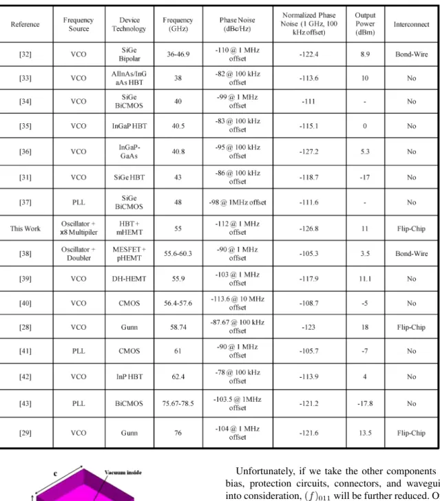
Table III summarizes the performance of the FC and bond-wire LO MCMs. The PN obtained for the FC-MCM frequency source is the lowest reported for -band frequency sources in the open literature [32]–[43]. A comparison to other publica-tions is given in Table IV, the results are bench-marked after the normalized PN presented in (2). The power consumption of the multiplier is in the order of 200 mW. Adding the power consumption of the oscillator, the total power consumption is still below 400 mW, yielding a PN-power FOM , which is excellent for a -band frequency source [31].
For applications, the assembled MMIC module has to be packaged into a metal house with coaxial connectors or wave-guide interfaces, which might cause instability of the output signal due to the cavity resonances. For a rectangular cavity, as shown in Fig. 23, the cavity resonances could happen in the following frequencies [44]:
(3) where is the material permittivity, is the material perme-ability, and and are integers. Here, the mode is the dominant mode since it occurs at the lowest frequency at which a cavity resonance can exist [45]. of the FC module and bond-wire module are found to be 43 and 48 GHz, respectively. This means that the resonances could occur if the
Fig. 23. Rectangular cavity with correspondinga; b; and c in (3).
operating frequencies of the modules are higher than 43 and 48 GHz. Due to smaller cavity size, of the bond-wire is higher than that of the FC. However, the bond-wire module excludes the other oscillator output for PLL implementation, which also occupies some additional space and increases the size of the bond-wire module. Moreover, the FC has a smaller footprint than the bond-wire. After considering these issues, we could expect the of the FC module would be higher than that of the bond-wire module.
Unfortunately, if we take the other components such as dc bias, protection circuits, connectors, and waveguide flanges into consideration, will be further reduced. One solution is aligning the MMICs in as narrow a row as possible, which results in higher resonance frequencies. Otherwise, another promising approach is using an absorber material to dampen the resonances [45].
It is worth mentioning that both the oscillator and multiplier chip have two circuits on the same chip. The module size can be reduced significantly if the circuits were separated by dicing.
VI. CONCLUSION
This work has successfully demonstrated FC assembly of a 7-GHz low PN cross-coupled HBT oscillator and a 8 mHEMT multiplier into an ultra-low PN -band MCM fre-quency source. It has been a shown that FC bonding is an excellent assembly technology for the implementation of mil-limeter-wave frequency sources. Compared with the bare-die
measurements, the FC technology does not have any detri-mental effect on the chip performance, neither for oscillators, nor for multipliers. On the contrary, the chip performance was improved. After the FC, the PN of the cross-coupled InGaP HBT oscillator was improved due to an increased factor of the resonant tank. A properly designed FC transition can also act as an additional matching network; an improved input and output matching was obtained for the 8 mHEMT multiplier chain using FC assembly. The FC assembled -band MCM frequency source exhibits a PN of 88 dBc/Hz @ 100-kHz offset and 112 dBc/Hz @ 1-MHz offset. To the authors’ best knowledge, this is the lowest PN ever reported for a -band free-running frequency source.
ACKNOWLEDGMENT
This research was carried out at the GigaHertz Centre, Chalmers University of Technology, Göteborg, Sweden. The authors would like to thank to C.-T. Wang and S.-P. Tsai, both with the Compound Semiconductor Laboratory, National Chiao-Tung University, Hsinchu, Taiwan, for their help with the Al O carrier fabrication.
REFERENCES
[1] P. Smulders, “Exploiting the 60 GHz band for local wireless multi-media access: Prospects and future directions,” IEEE Commun. Mag., vol. 40, no. 1, pp. 140–147, Jan. 2002.
[2] V. Dyadyuk, J. D. Bunton, J. Pathikulangara, R. Kendall, O. Sevimli, L. Stokes, and D. A. Abbott, “A multigigabit millimeter-wave communi-cation system with improved spectral efficiency,” IEEE Trans. Microw.
Theory Tech., vol. 55, no. 12, pp. 2813–2821, Dec. 2007.
[3] C. Kärnfelt, R. Kozhuharov, H. Zirath, and I. Angelov, “High-purity 60-GHz-band single-chip 28 multipliers in pHEMT and mHEMT technology,” IEEE Trans. Microw. Theory Tech., vol. 54, no. 6, pp. 2887–2898, Jun. 2006.
[4] H. Zirath, R. Kozhuharov, and M. Ferndahl, “Balanced colpitt oscil-lator MMICs designed for ultra-low phase noise,” IEEE J. Solid-State
Circuits, vol. 40, no. 10, pp. 2077–2086, Oct. 2005.
[5] K. K. Samanta, D. Stephens, and I. D. Robertson, “60 GHz multi-chip-module receiver with substrate integrated waveguide antenna and filter,” Electron. Lett., vol. 42, pp. 701–702, Jun. 2006.
[6] L. Suthar, V. N. Singh, and A. Kumar, “Design & simulation of MCM technology based MM wave transceiver,” in Int. Recent Adv. Microw.
Theory Appl. Conf. , Jaipur, India, Nov. 2008, pp. 533–535, 21–24.
[7] J. Heyen and A. F. Jacob, “A novel package approach for multichip modules based on anisotropic conductive adhesives,” in Eur. Gallium
Arsenide Other Semicond. Appl. Symp., Oct. 3–4, 2005, pp. 553–556.
[8] G. Baumann, H. Richter, A. Baumgärtner, D. Ferling, and R. Heilig, “51 GHz front-end with flip-chip and wire bond interconnections from GaAs MMIC’s to a planar patch antenna,” in IEEE MTT-S Int. Microw.
Symp. Dig., Orlando, FL, May 16–20, 1995, vol. 3, pp. 1639–1642.
[9] C. L. Wang and R. B. Wu, “Modeling and design for electrical per-formance of wideband flip-chip transition,” IEEE Trans. Adv. Packag., vol. 26, no. 4, pp. 385–391, Nov. 2003.
[10] K. Maruhashi, M. Ito, H. Kusamitsu, Y. Morishita, and K. Ohata, “RF performance of a 77 GHz monolithic CPW amplifier with flip-chip in-terconnections,” in IEEE MTT-S Int. Microw. Symp. Dig., Baltimore, MD, Jun. 7–12, 1998, vol. 2, pp. 1095–1098.
[11] A. Jentzsch and W. Heinrich, “Theory and measurements of flip-chip interconnects for frequencies up to 100 GHz,” IEEE Trans. Microw.
Theory Tech., vol. 49, no. 5, pp. 871–878, May 2001.
[12] D. Staiculescu, J. Laskar, and E. M. Tentzeris, “Design rule devel-opment for microwave flip-chip applications,” IEEE Trans. Microw.
Theory Tech., vol. 48, no. 9, pp. 1476–1481, Sep. 2000.
[13] Z. Feng, W. Zhang, B. Su, K. C. Gupta, and Y. C. Lee, “RF and me-chanical characterization of flip-chip interconnects in CPW circuits with underfill,” IEEE Trans. Microw. Theory Tech., vol. 46, no. 12, pt. 2, pp. 2269–2275, Dec. 1999.
[14] H. Kusamitsu, Y. Morishita, K. Maruhasi, M. Ito, and K. Ohata, “The flip-chip bump interconnection for millimeter-wave GaAs MMIC,”
IEEE Trans. Electron., Packag., Manuf., vol. 22, no. 1, pp. 23–28, Jan.
1999.
[15] W. C. Wu, H. T. Hsu, E. Y. Chang, C. S. Lee, C. H. Huang, Y. C. Hu, L. H. Hsu, and Y. C. Lien, “Flip-chip packaged In Al As/InGaAs metamorphic HEMT device for millimeter wave application,” in Proc.
CS-MAX, Compound Semicond. Manuf. Expo., Palm Spring, CA, Nov.
2005, pp. 94–97.
[16] J. H. Lau, “Cost analysis: Solder bumped flip chip versus wire bonding,” IEEE Trans. Electron., Packag., Manuf., vol. 23, no. 1, pp. 4–11, Jan. 2000.
[17] D. Kuylenstierna, H. Zirath, R. Kozuharov, M. Bao, and T. C. Tsai, “Low phase noise MMIC oscillators in InGaP HBT technology,” in
Asia–Pacific Microw. Conf., Hong Kong, Dec. 2008, pp. 1–4.
[18] Y. K. Song and C. C. Lee, “Flip-chip packaging configuration with coplanar strip lines for millimeter electromagnetic waves,” in 56th
Proc. Electron. Compon. Technol. Conf., San Diego, CA, 2006, pp.
1700–1705.
[19] N. Jayesh and S. Soora, “Design and optimization of coax-to-mi-crostrip transition and through-hole signal via on multilayer printed circuit boards,” in Eur. Microw. Conf., Munich, Germany, Oct. 9–12, 2007, pp. 134–137.
[20] D. Peyrou, P. Pons, A. Nicolas, J.-W. Tao, H. Granier, and R. Plana, “Foturan cap and BCB sealing-ring for RF MEMS packaging applica-tions,” in 1st Eur. Microw. Integr. Circuits Conf., Manchester, U.K., Sep. 10–13, 2006, pp. 456–459.
[21] A. Hajimiri and T. H. Lee, “Design issues in CMOS differentialLC oscillators,” IEEE J. Solid-State Circuits, vol. 34, no. 5, pp. 717–724, May 1999.
[22] X. Huo, G.-W. Xiao, P. C. H. Chan, and K. J. Chen, “Silicon-on-or-ganic integration of a 2.4-GHz oscillator using high-Q copper induc-tors and solder-bumped flip chip technology,” IEEE Trans. Compon.
Packag. Technol., vol. 32, no. 1, pp. 191–196, Mar. 2009.
[23] K. Stadius and K. Halonen, “Development of 4-GHz flip-chip oscillator module,” in IEEE Int. Circuits Syst. Symp., Kobe, Japan, May 23–26, 2005, vol. 3, pp. 2687–2690.
[24] Y. M. Hsin, Y. A. Liu, C. M. Wang, W. K. Huang, and T. J. Yeh, “27 GHz flip-chip assembled pHEMT oscillator,” in Proc. CS-MAX,
Com-pound Semicond. Manuf. Expo., Vancouver, BC, Canada, Apr. 24–27,
2006, pp. 127–129.
[25] W. K. Huang, Y. A. Liu, C. M. Wang, Y. M. Hsin, C. Y. Liu, and T. J. Yeh, “Flip-chip assembled GaAs pHEMTKa-band oscillator,” IEEE
Microw. Wireless Compon. Lett., vol. 17, no. 1, pp. 67–69, Jan. 2007.
[26] M. Ito, K. Maruhashi, S. Kishimoto, T. Hashiguchi, and K. Ohata, “A 30 GHz-band oscillator coupled with a dielectric resonator using flip-chip bonding technique,” in IEEE MTT-S Int. Microw. Symp. Dig., Fort Worth, TX, Jun. 6–11, 2004, vol. 3, pp. 1995–1998.
[27] T. Yoshida, T. Deguchi, K. Kawaguchi, and A. Nakagawa, “Ka-band planar Gunn oscillators using flip-chip GaAs Gunn diodes fabricated by boron ion implantation,” in 22nd Annu. Gallium Arsenide Integr.
Circuit Symp., Seattle, WA, Nov. 5–8, 2000, pp. 165–168.
[28] K. Watanabe, T. Deguchi, and A. Nakagawa, “V -band planar Gunn oscillators and VCOs on AlN substrates using flip-chip bonding tech-nology,” in IEEE MTT-S Int. Microw. Symp. Dig., Anaheim, CA, Jun. 13–19, 1999, vol. 1, pp. 13–16.
[29] T. Yoshida, Y. Fukasawa, T. Deguchi, K. Kawaguchi, T. Sugiyama, and A. Nakagawa, “A low-phase-noise 76-GHz planar Gunn oscil-lator using flip-chip bonding technology,” in Eur. Microw. Conf., Paris, France, Oct. 4–6, 2005, vol. 1.
[30] D. B. Leeson, “A simple model of feedback oscillator noise spectrum,”
Proc. IEEE, vol. 54, no. 2, pp. 329–330, Feb. 1966.
[31] M. Q. Bao, Y. G. Li, and H. Jacobsson, “A 21.5/43-GHz dual-fre-quency balanced Colpitts VCO in SiGe technology,” IEEE J.
Solid-State Circuits, vol. 39, no. 8, pp. 1352–1355, Aug. 2004.
[32] H. Li and H. M. Rein, “Millimeter-wave VCOs with wide tuning range and low phase noise, fully integrated in a SiGe bipolar production tech-nology,” IEEE J. Solid-State Circuits, vol. 38, no. 2, pp. 184–191, Feb. 2003.
[33] A. Kurdoghlian, M. Sokolich, M. Case, M. Micovic, S. Thomas, III, and C. H. Fields, “38 GHz low phase noise CPW monolithic VCOs implemented in manufacturable AlInAs/InGaAs HBT IC technology,” in 22nd Annu. Gallium Arsenide Integr. Circuit Symp., Seattle, WA, Nov. 5–8, 2000, pp. 99–102.
[34] D. K. Shaeffer and S. Kudszus, “Performance-optimized microstrip coupled VCOs for 40-GHz and 43-GHz OC-768 optical transmission,”
Nov. 1995, pp. 259–262.
[39] T. Kashiwa, T. Ishida, T. Katoh, H. Kurusu, H. Hoshi, and Y. Mitsui, “V -band high-power low phase-noise monolithic oscillators and inves-tigation of low phase-noise performance high drain bias,” IEEE Trans.
Microw. Theory Tech., vol. 46, no. 10, pp. 1559–1565, Oct. 1998.
[40] P. C. Huang, M. D. Tsai, G. D. Vendelin, H. Wang, C. H. Chen, and C. S. Chang, “A low-power 114-GHz push–push CMOS VCO usingLC source degeneration,” IEEE J. Solid-State Circuits, vol. 42, no. 6, pp. 1230–1239, Jun. 2007.
[41] T. Mitomo, R. Fujimoto, N. Ono, R. Tachibana, H. Hoshino, Y. Yoshi-hara, Y. Tsutsumi, and I. Seto, “A 60-GHz CMOS receiver front-end with frequency synthesizer,” IEEE J. Solid-State Circuits, vol. 43, no. 4, pp. 1030–1037, Apr. 2008.
[42] H. Wang, K. W. Chang, D. C.-W. Lo, L. T. Tran, J. C. Cowles, T. R. Block, G. S. Dow, A. Oki, D. C. Streit, and B. R. Allen, “A 62-GHz monolithic InP-based HBT VCO,” IEEE Microw. Guided Wave Lett., vol. 5, no. 11, pp. 388–390, Nov. 1995.
[43] V. Jain, B. Javid, and P. Heydari, “A 24/77 GHz dual-band BiCMOS frequency synthesizer,” in IEEE Custom Integr. Circuits Conf., San Jose, CA, Sep. 21–24, 2008, pp. 487–490.
[44] R. Harrington, Time Harmonic Electromagnetic Fields. New York: McGraw-Hill, 1961, pp. 155–158.
[45] P. Dixon, “Cavity-resonance dampening,” IEEE Microw. Mag., vol. 6, no. 2, pp. 74–84, Jun. 2005.
Li-Han Hsu was born in Tainan, Taiwan, in 1981. He received the B.S. and M.S. degrees in materials science and engineering from the National Chiao Tung University, Hsinchu, Taiwan, in 2003 and 2005, respectively, and is currently working toward the dual Ph.D. degrees in materials science and engi-neering at National Chiao Tung University, Hsinchu, Taiwan and in microtechnology and nanoscience at MC2, Chalmers University of Technology, Göte-borg, Sweden.
His main research interest is millimeter-wave packaging technology including flip-chip interconnects, hot-via interconnects, and integration ofV -/E-band MCM transceiver modules.
Dan Kuylenstierna (S’04) was born in Göteborg, Sweden, in 1976. He received the M.Sc. degree in physics and engineering physics and Ph.D. degree in electrical engineering in microtechnology and nanoscience from the Chalmers University of Tech-nology, MC2, Göteborg, Sweden, in 2001 and 2007, respectively.
His main scientific interests are frequency genera-tion, MMIC design, packaging technologies, and re-configurable MMICs.
Dr. Kuylenstierna was the recipient of the Second Prize of the Student Paper Award Competition at the 2004 IEEE Microwave Theory and Techniques Society (IEEE MTT-S) International Microwave Sym-posium (IMS).
1998, he became a Senior Research Associate with the Institute of Electronics. He was a Visiting Researcher for a short time with the University “Claude Bernard” (microwave industrial applications), Lyon, France (1981), the In-stitute of Radiolectronics, Prage, Czech Republic (1987–1989), and with the Chalmers University, Göteborg, Sweden (1996–2000). Since 2000, he has been with the Department of Microtechnology and Nanoscience (MC2), Chalmers University of Technology, where he has been involved with the design and investigation of low-noise hybrid oscillators, stabilized with HTSC resonators, HEMT and HBT MMIC millimeter-wave VCOs and multipliers for high data rate communication links, and MMIC W - and G-band front-end receivers for radiometers measuring and imaging applications. He has authored or coauthored over 70 papers in international journals and conference proceedings and one book. He holds one patent.
Marcus Gavell was born in Eskilstuna, Sweden, 1981. He received the M.Sc. degree in electrical engineering from the Chalmers University of Tech-nology, Göteborg, Sweden, in 2005.
In 2007, he joined the Department of Microtech-nology and Nanoscience, Chalmers University of Technology, following two years as a Consultant, initially involved with electric power distribution with Projektel AB and then as a Verification En-gineer with Ericsson AB. His research interests concern millimeter-wave MMIC design and building practice.
Camilla Kärnfelt (M’05) was born in Dragsmark, Sweden, in 1965. She received the M.Sc. degree in engineering physics from the Chalmers University of Technology, Göteborg, Sweden, in 2001.
From 1987 to 2001, she was with Ericsson Mi-crowave Systems as a Preproduction Engineer with a specialization in microwave hybrid manufacturing. In September 2001, she joined the startup company Optillion as a Research Engineer. From 2002 to 2007, she was with the Microwave Electronics Laboratory, Chalmers University of Technology, as a Research Engineer. She is currently with the Microwave Départment, Télécom Bretagne, Brest, France. Her research interests concern millimeter-wave MMIC design.
Wee-Chin Lim was born in Johor, Malaysia, in 1986. She received the B.S. degree in materials science from the National University of Malaysia (UKM), Kuala Lumpur, Malaysia, in 2008, and is currently working toward the Master degree’s student in materials science and engineering at the National Chiao Tung University (NCTU), Hsinchu, Taiwan.
She is currently a member of the Compound Semi-conductor Device Laboratory, National Chiao Tung University (NCTU), Hsinchu, Taiwan.
Herbert Zirath (S’84–M’86–SM’08) was born in Göteborg, Sweden, on March 20, 1955. He received the M.Sc. and Ph.D. degrees from Chalmers Univer-sity of Technology, Göteborg, Sweden, in 1980 and 1986, respectively.
He is currently a Professor of High Speed Elec-tronics with the Department of Microtechnology and Nanoscience, Chalmers University of Technology. During 2001, he became the Head of the Microwave Electronics Laboratory, Chalmers University of Technology. He currently leads a group of approx-imately 30 researchers in the area of high-frequency semiconductor devices and circuits. He has authored or coauthored over 220 papers in international journals and conference proceedings and one book. He holds four patents. His main research interests include InP-HEMT devices and circuits, SiC- and GaN-based transistors for high-power applications, device modeling including noise and large-signal models for FET and bipolar devices, and foundry-related monolithic microwave ICs for millimeter-wave applications based on both III–V and silicon devices. He also works part-time with Ericsson AB, Mölndal, Sweden, as a Microwave Circuit Expert.
Edward Yi Chang (S’85–M’85–SM’04) received the B.S. degree in materials science and engineering from National Tsing Hua University, Hsinchu, Taiwan, in 1977, and the Ph.D. degree in materials science and engineering from the University of Minnesota at Minneapolis–St. Paul, in 1985.
From 1985 to 1988, he was with the GaAs Compo-nent Group, Unisys Corporation, Eagan, MN. From 1988 to 1992, he was with the Comsat Labs Micro-electronic Group. He was involved with GaAs MMIC programs with both groups. In 1992, he was with Na-tional Chiao Tung University (NCTU), Hsinchu, Taiwan. In 1994, he helped set up the first GaAs MMIC production line in Taiwan, and in 1995, became the President of Hexawave Inc., Hsinchu, Taiwan. In 1999, he returned to NCTU with a teaching position, where he is currently a Professor with the Department of Materials Science and Engineering. His research interests include new de-vice and process technologies for compound semiconductor RFICs for wireless communication.
Dr. Chang is a Senior Member and a Distinguished Lecturer of the IEEE Electronic Device Society.