H
2and NH
3Plasma Passivation on Poly-Si TFTs
with Bottom-Sub-Gate Induced Electrical Junctions
Cheng-Ming Yu,a Horng-Chih Lin,b,zTiao-Yuan Huang,a,band Tan-Fu Leia aInstitute of Electronics, National Chiao-Tung University, Hsinchu, Taiwan 30050
b
National Nano Device Laboratories, Hsinchu, Taiwan 30050
The effects of NH3and H2 plasma passivation on the characteristics of poly-Si thin-film transistors共TFTs兲 with source/drain extensions induced by a bottom sub-gate were studied. Our results show that although significant improvements in device performance can be obtained by either passivation method, the NH3-plasma-treatment appears to be more effective in reducing the off-state leakage, subthreshold swing, and in improving mobility compared to H2plasma passivation. Furthermore, NH3plasma treatment is also found to be more effective in reducing the anomalous subthreshold hump phenomenon observed in nonplasma-treated short-channel devices. Detailed analysis suggests that all these improvements can be explained by the more effective passivation of traps distributed in both the front and back sides of the channel by NH3plasma treatment.
© 2003 The Electrochemical Society. 关DOI: 10.1149/1.1627355兴 All rights reserved.
Manuscript submitted December 9, 2002; revised manuscript received June 26, 2003. Available electronically November 3, 2003.
Recently, polycrystalline silicon 共poly-Si兲 thin-film transistors 共TFTs兲 have received lots of attention as replacements for amor-phous silicon TFTs in the switching elements of high-performance large-area active-matrix display and sensor systems. With their higher mobility, the peripheral driver circuitry can be integrated on the same substrate, which further improves system performance and reliability.1,2 However, defects at the grain boundaries as well as inside the grains are known to cause device degradation,3resulting in poor device performance including low mobility and high off-state leakage current.4,5In order to obtain high-performance poly-Si TFTs, it is essential to reduce the trap density in the poly-Si channel. To this end, hydrogen plasma passivation is a well-known technique.6,7 The atomic hydrogen can passivate defects in the poly-Si channel, thereby improving device characteristics. In addi-tion, nitrogen-containing plasma treatments in combination with hy-drogen共e.g., H2/N2mixture plasma,8nitrogen implantation with H2
plasma,9 preoxidation NH3 annealing with H2 plasma,10and NH3
plasma11兲 have also been shown to further improve the device per-formance. The additional nitrogen passivation and/or the enhanced hydrogen passivation effects in the presence of nitrogen are presum-ably responsible for the observed improved characteristics.
Another approach for reducing the off-state leakage current is to use an electrical drain junction that is induced by a sub-gate.12,13It has been shown that with proper device structure design and opera-tion condiopera-tions, the leakage current can be dramatically reduced without significantly compromising the drive current. Conventionally,12a top sub-gate configuration is used. Recently, we have proposed a novel TFT device with bottom sub-gate configuration.13,14In previous work we have explored and charac-terized the fabricated devices and shown that high device perfor-mance could be achieved using this structure. In this work, we fur-ther explore and compare the effects of plasma treatments in NH3or
H2ambient on device characteristics.
Experimental
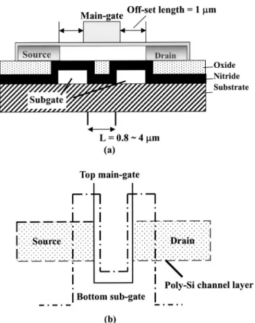
Figure 1 shows the cross-sectional and top views of the poly-Si TFT used in this experiment. The fabricated devices feature a top main gate and a fork-shaped bottom gate. The fork-shaped sub-gate has two split branches buried under the poly-Si active layer used for electrically inducing the source and drain extensions. The device’s channel length, L, is thus defined by the spacing between the two branches of the sub-gate. The length of the offset channel regions between the implanted source/drain and the main gate is fixed at 1m in this study.
The key process flow for fabricating the poly-Si TFTs with bot-tom sub-gate was described in detail in our previous work.13,14 Briefly, a 100 nm n⫹-poly-Si layer was deposited on an oxidized silicon substrate by low-pressure chemical vapor deposition 共LPCVD兲. The doped poly-Si film was then patterned to form the fork-shaped bottom sub-gate. Next, a 100 nm nitride layer was de-posited by chemical vapor deposition共CVD兲, followed by the depo-sition of a thick low-pressure tetraethyl orthosilicate共550 nm兲 oxide layer. Chemical mechanical polishing 共CMP兲 was then applied to planarize the wafer surface and to expose the nitride layer on top of the sub-gate. It is worthy to note that the nitride layer serves not only as the dielectric separation between the field-plate 共i.e., sub-gate兲 and the active device layer in the final device structure, it also
zE-mail: [email protected]
Figure 1. 共a兲 Cross-sectional and 共b兲 top views of a TFT device with bottom sub-gate.
serves as an etch stopper for the CMP process. Afterward, a 50 nm CVD amorphous Si film was deposited at 550°C, which was subse-quently converted to polycrystalline phase by solid-phase crystalli-zation共SPC兲 at 600°C for 24 h, to serve as the active device layer. A 20 nm CVD oxide layer was then deposited to form the gate insu-lator. An n⫹poly-Si film was deposited and patterned to form the
top main-gate. Next, the offset source/drain regions were defined by a photoresist masking step before performing the source/drain ion implantation. For n-channel transistors, As⫹implant with a dosage of 5⫻ 1015cm⫺2at 20 keV was used. Similarly, BF
2
⫹implant with a dosage of 5⫻ 1015cm⫺2at 30 keV was used for p-channel
tran-sistors. The implanted dopants were subsequently activated in N2
ambient at 600°C for 12 h. Wafers then followed a standard back-end processing for contact pad formation and metallization. Finally, some devices were split to receive NH3or H2plasma treatment in a
parallel-plate plasma reactor at 250°C for 3 h.
Results and Discussion
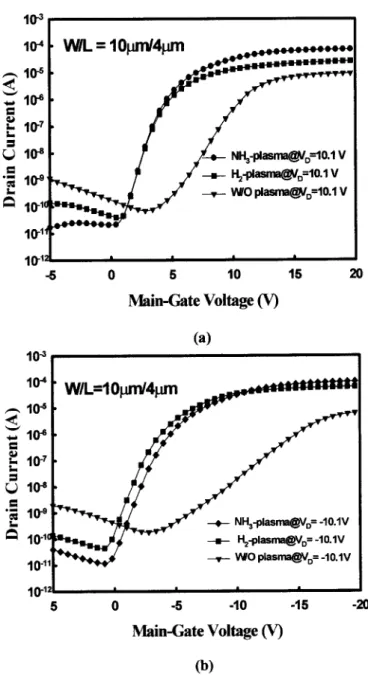
Characteristics of long-channel devices.—Figure 2 compares the subthreshold characteristics of devices with and without plasma treatment. The channel length and width of the devices are 4 and 10 m, respectively. Note that a fixed sub-gate bias of 40 V was chosen in this work because it is large enough for the device performance improvement, while small enough not to degrade the reliability of the dielectric underneath the sub-gate. Tables I and II summarize several important parameters, including subthreshold swing S, threshold voltage Vth, trap-state density Nt, off-state leakage cur-rent Ioff, and on/off current ratio, extracted from the results shown
in Fig. 2. The threshold voltage is defined at a fixed drain current ID⫽ IDN⫻ W/L,15 where IDN is 10 nA. Extraction of trap-state
densities is performed using the modified Levinson’s method.16,17 From these results, it can be seen that significant improvements are achieved for both n- and p-channel devices treated by either H2or
NH3 plasma, though in the latter case the improvements are much
larger. This is further highlighted in Fig. 3 in which the ID-VD
char-acteristics of n- and p-channel TFTs are shown共nTFT and pTFT, respectively兲. Clearly, NH3-plasma-treated samples show better
per-formance, especially for n-channel devices.
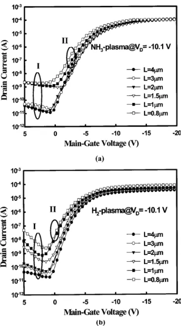
Dependence of channel length.—The effects of channel length on device performance for n- and p-channel devices are shown in Fig. 4 and 5, respectively. From these results, two basic leakage components are identified: (i) the off-state leakage current that in-creases with increasing voltage difference between the gate and drain (VGD) as L⬍ 2 m, and (ii) the ‘‘hump’’ that appears in the
subthreshold regionas L⬍ 1.5 m. The former component is well characterized in the literature and could be ascribed to the trap-assisted thermionic emission5 or field emission18 conduction pro-cess. Such leakage process is closely related to the amount of trap density in the channel. Note that due to the bottom sub-gate con-figuration in the devices, the flow path for such leakage component is from the surface channel to the bottom extension drain junction, as schematically shown in Fig. 6共path 1兲. To highlight the impor-tance of the sub-gate bias on this type of leakage, Fig. 7 depicts the off-state leakage for both p- and n-channel devices treated with NH3
plasma as a function of the sub-gate bias. In the measurements, the main-gate voltages are fixed at⫺5 and 5 V for n- and p-channel operations, respectively. It can be seen that the leakage is roughly constant in the low-sub-gate bias region, and starts to rise when the Figure 2. Subthreshold (ID-VG) characteristics of 共a兲 n-channel and 共b兲
p-channel TFTs with different plasma treatments. The sub-gate biases of nTFT and pTFT are 40 and⫺40 V, respectively.
Table I. The values of SS, Vth, Nt, Ioff, and onÕoff current ratio of the n-channel polysilicon TFTs for various plasma treatments.
Plasma gas Subthreshold swing 共V/dec兲 共V兲Vth Nt (⫻1011cm⫺2) V Ioff共A兲 D⫽ 10.1 V Ion/Ioff VD⫽ 10.1 V No plasma treatment 1.62 13 22.1 3.78⫻ 10⫺11 1.1⫻ 105 H2-plasma treatment 0.72 4 9.59 3.77⫻ 10⫺11 7.1⫻ 105 NH3-plasma treatment 0.64 3.4 7.63 1.7⫻ 10⫺11 4.4⫻ 106
sub-gate voltage exceeds a threshold, e.g., around 15 V for nTFT and⫺20 V for pTFT, corresponding to the formation of electrical drain extension in the offset region.
At a fixed channel length, the leakage for H2-plasma-treated
de-vices is higher than the NH3-plasma-treated ones, as can be seen in
Fig. 4 and 5. This again indicates that NH3plasma is more effective
in passivating the defects in the poly-Si channel. This is further confirmed with the results shown in Fig. 8, in which the extracted effective trap-state density (Nt) using the modified Levinson’s
method17is plotted as a function of channel length. Note that these results are for the unpassivated defects located at or near the front-side interface in which an inversion layer formation is taking place. It is observed that the Ntvalues for NH3-plasma-treated devices are
lower than H2-plasma-treated counterparts. Moreover, there is a
re-Figure 3. Output (ID-VD) characteristics of共a兲 n-channel and 共b兲 p-channel TFTs with different plasma treatments. The sub-gate biases of nTFT and pTFT are 40 and⫺40 V, respectively.
Figure 4. Subthreshold characteristics of n-channel TFT devices with
vari-ous channel lengths at VD⫽ 10.1 V after 共a兲 NH3plasma treatment and共b兲 H2plasma treatment. The sub-gate bias is 40 V.
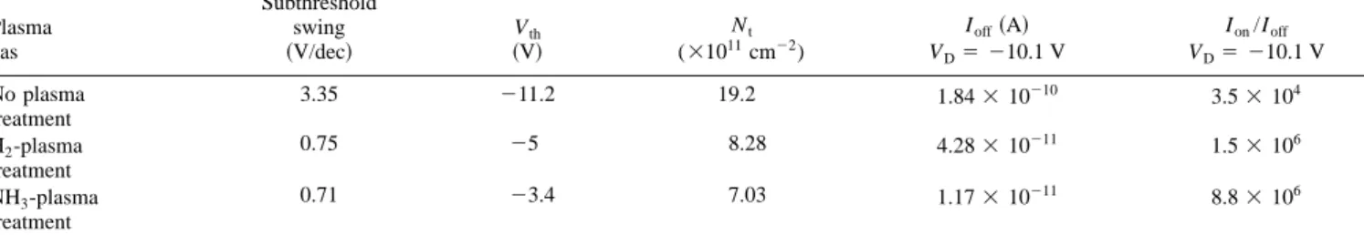
Table II. The values of SS, Vth, Nt, Ioff, and onÕoff current ratio of the p-channel polysilicon TFTs for various plasma treatments.
Plasma gas Subthreshold swing 共V/dec兲 共V兲Vth Nt (⫻1011cm⫺2) Ioff共A兲 VD⫽ ⫺10.1 V Ion/Ioff VD⫽ ⫺10.1 V No plasma treatment 3.35 ⫺11.2 19.2 1.84⫻ 10⫺10 3.5⫻ 104 H2-plasma treatment 0.75 ⫺5 8.28 4.28⫻ 10⫺11 1.5⫻ 106 NH3-plasma treatment 0.71 ⫺3.4 7.03 1.17⫻ 10⫺11 8.8⫻ 106
duction in Nt for devices having a shorter channel. This trend is reasonable because the passivation of defects in the channel is re-lated to the diffusion of passivating species from the edge of the channel. Devices with a shorter length may have more defects pas-sivated in the middle of the channel simply because of a shorter diffusion path.19Nevertheless, the off-state leakage becomes signifi-cant as L⬍ 2 m because of the dramatic increase in field strength. The appearance of a hump in the subthreshold region as L⬍ 1.5 m has been reported in our previous report.14The leakage path is believed to flow through the back-side surface of the channel layer, as illustrated in Fig. 6共path 2兲. Some defects near the bottom interface generated during some processing steps共e.g., CMP兲 are believed to be responsible for such leakage. Such phenomenon also leads to the anomalous current increase in the output characteristics of short-channel devices, as shown in Fig. 9. By comparing the device characteristics, the hump is less pronounced in NH3-plasma-treated samples, implying that the NH3plasma is also
more effective in reducing the active defect density along the back-side surface of the channel layer.
From these observations, it is clear that NH3 plasma is more
effective in passivating trap state and improving device characteris-tics. This may be due to the appearance of nitrogen species in the NH3plasma that may also help passivate the defects. According to a
previous report,11the use of NH3plasma treatment would result in
the nitrogen pileup at the SiO2/poly-Si interface and the formation
Figure 5. Subthreshold characteristics of p-channel TFT devices with
vari-ous channel lengths at VD⫽ ⫺10.1 V after 共a兲 NH3plasma treatment and
共b兲 H2plasma treatment. The sub-gate bias is⫺40 V.
Figure 6. Illustration of the leakage path along the top共path 1兲 and bottom 共path 2兲 interfaces of the poly-Si active layer.
Figure 7. Off-state drain current as a function of sub-gate bias for共a兲 n- and 共b兲 p-channel TFTs with NH3-plasma treatment.
of strong Si-N bonds, which tends to terminate the dangling bonds in the grains and at the grain boundaries in the poly-Si channel. In our case, these events could occur at or near both top and bottom interfaces, and thus result in the reduction of off-state leakage.
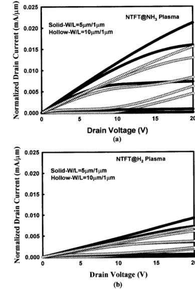
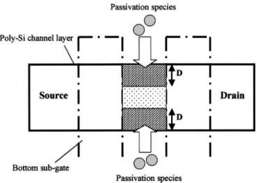
Dependence of channel width.—In order to understand the cause of hump phenomenon in more detail, transistors having same chan-nel length共1 m兲 but different channel width were characterized and compared. The effects of channel width on device output char-acteristics for n- and p-channel devices are shown in Fig. 10 and 11, respectively. Note that the current has been normalized to the chan-nel width. In these figures we can see that significant increase in output current could be realized as channel width is reduced. Mean-while, the aforementioned anomalous phenomenon in current-voltage characteristics becomes less pronounced and eventually dis-appears as channel width is reduced. The improvement in device performance could be correlated with the diffusion path of the pas-sivation species, as schematically shown in Fig. 12. To more clearly illustrate the situation, the top gate is deliberately not shown in the figure. Because the passivation species enter the device region from the edges of the channel, defect passivation takes place initially at the edges of the channel and then gradually extends to the central region away from the channel edges. For devices with a wider chan-nel, the defects located at the central region may remain unpassi-vated after the plasma treatment. The unpassiunpassi-vated defects at the bottom central channel interface are believed to be responsible for Figure 8. Trap-state density vs. gate length for n- and p-channel TFTs with
H2- and NH3-plasma treatments.
Figure 9. Comparison of output characteristics for H2- and NH3-plasma passivated共a兲 n-channel and 共b兲 p-channel devices with L ⫽ 0.8 m. The sub-gate biases of nTFT and pTFT are 40 and⫺40 V, respectively.
Figure 10. Output characteristics of nTFT devices with various channel
the hump phenomenon observed in short-channel devices. When the width is narrow enough共e.g., ⭐5 m), the passivation process is complete 共i.e., even the central channel region has become fully passivated兲 after the plasma treatment, so the leakage could be ef-fectively suppressed.
Conclusions
In this work, TFT devices with electrical source/drain extensions induced by a bottom sub-gate after treatment in H2or NH3plasma
were characterized. NH3plasma was found to be more effective than
H2 plasma for passivating defects in the poly-Si channel, thus
re-sulting in lower off-state current, steeper subthreshold slope, and lower threshold voltage. The hump phenomenon observed in short-channel TFTs indicates the existence of an additional leakage path formed on the bottom interface of the channel layer. Our results indicate that NH3plasma passivation is also more effective in
sup-pressing such phenomenon. Moreover, the effects of channel width on the characteristics of both n- and p-type hydrogenated devices were investigated. It is shown that the hump in current-voltage char-acteristics could be effectively suppressed for devices with narrow channel width.
Acknowledgments
The authors thank the staff at National Nano Device Laboratories for their assistance in device fabrication. This work was supported in part by the National Science Council of the Republic of China under contract no. NSC-90-2721-2317-200.
National Chiao-Tung University assisted in meeting the publication costs of this article.
References
1. I. W. Wu, Tech. Dig. Active Matrix Liquid Crystal Display, 1995, 7.
2. T. Serikawa, S. Shirai, A. Okamoto, and S. Suyama, IEEE Trans. Electron Devices,
36, 1929共1989兲.
3. I. W. Wu, W. B. Jackson, T. Y. Huang, A. G. Lewis, and A. Ciang, IEEE Electron
Device Lett., 12, 181共1991兲.
4. W. G. Hawkins, IEEE Trans. Electron Devices, 33, 477共1986兲.
5. J. G. Fossum, A. O. Conde, H. Shichijo, and S. K. Banerjee, IEEE Trans. Electron
Devices, 33, 1518共1986兲.
6. K. Baert, H. Murai, K. Kobayashi, H. Namizaki, and M. Nunoshita, Jpn. J. Appl.
Phys., Part 1, 32, 2601共1993兲.
7. A. Yin and S. J. Fonash, IEEE Electron Device Lett., 15, 502共1994兲.
8. M. J. Tsai, F. S. Wang, K. L. Cheng, S. Y. Wang, M. S. Feng, and H. C. Chen,
Solid-State Electron., 38, 1233共1995兲.
9. C. K. Yang, T. F. Lei, and C. L. Lee, Tech. Dig. Int. Electron Devices Meet., 1994, 505.
10. C. K. Yang, T. F. Lei, and C. L. Lee, IEEE Electron Device Lett., 15, 389共1994兲. 11. H. C. Cheng, F. S. Wang, and C. Y. Huang, IEEE Trans. Electron Devices, 44, 64
共1997兲.
12. T. Y. Huang, I. W. Wu, A. G. Lewis, A. Chiang, and R. H. Bruce, IEEE Electron
Device Lett., 11, 244共1990兲.
13. H. C. Lin, M. Yu, C. Y. Lin, K. L. Yeh, T. Y. Huang, and T. F Lei, IEEE Electron
Device Lett., 22, 26共2001兲.
14. M. Yu, H. C. Lin, G. H. Chen, T. Y. Huang, and T. F. Lei, Jpn. J. Appl. Phys., Part
1, 5A, 41, 1共2002兲.
15. A. G. Lewis, Tech. Dig. Int. Electron Devices Meet., 1988, 260.
16. J. Levinson, F. R. Shepherd, P. J. Scanlon, W. D. Westwood, G. Este, and M. Rider,
J. Appl. Phys., 53, 1193共1982兲.
17. R. E. Proano, R. S. Misage, and D. G. Ast, IEEE Trans. Electron Devices, 40, 2301 共1993兲.
18. S. K. Madan and D. A. Antoniadis, IEEE Trans. Electron Devices, 33, 1518共1986兲. 19. W. B. Jackson, N. M. Johnson, C. C. Tsai, I. W. Wu, A. Chiang, and D. Smith,
Appl. Phys. Lett., 61, 1670共1992兲. Figure 11. Output characteristics of pTFT devices with various channel
widths after共a兲 NH3 and 共b兲 H2 plasma treatment. The sub-gate bias is
⫺40 V.
Figure 12. Illustration of the diffusion process for passivation species dur-ing plasma treatment.
![[102-2] WNFA lab4 - A Tiny Wireless Sensor Network](data:image/gif;base64,R0lGODlhAQABAIAAAP///wAAACH5BAEAAAAALAAAAAABAAEAAAICRAEAOw==)