IEEE JOURNAL OF SOLID-STATE CIRCUITS, VOL. 24, NO. 3, J U N E 1989 779
CMOS Nonthreshold Logic (NTL) and
Cascode Nonthreshold Logic (CNTL)
for High-speed Applications
JINN-SHYAN WANG, MEMBER, IEEE, CHUNG-YU w u , MEMBER, IEEE,AND MING-KAI TSAI, MEMBER, IEEE
Ahtract -Two new high-speed CMOS logic circuits are proposed and analyzed. One is called the CMOS nonthreshold logic (CMOS NTL), the other the C M O S cascode nonthreshold logic (CMOS CNTL). The CMOS NTL is derived from its bipolar counterpart, which is the fastest bipolar logic, and takes the NOR gate as its basic building gate. It is shown that by applying the nonthreshold principle to CMOS circuits the resultant speed performance can also be highly promoted, but with a sacrifice of dc power consumption. From transient analyses the speed of CMOS NTL is found quite comparable to that of 12L or even ECL and is about 20-60 percent better than that of the conventional CMOS. Meanwhile, the power-delay product of C M O S NTL is smaller than those of 12L and ECL and is nearly the same as that of conventional CMOS operated at high frequency. The C M O S NTL was fabricated and measured, and experimental results have verified its performance.
The nonthreshold principle is then applied to the CMOS cascode structure to form the CMOS CNTL, in which there is a trade-off between speed performance and power dissipation. It is shown from the design of full adders that the CMOS NTL is the fastest of all the static CMOS logic circuits. The speed of the CNTL circuit, although slower than that of the NTL circuit, is still higher than that of the differential split-level logic (DSL) circuit, which is the fastest static circuit proposed so far. The CNTL circuit also has a smaller power-delay product than the DSL circuit.
The C M O S NTL and CNTL circuits can be used along with conven- tional C M O S circuits, and they are expected to increase the design flexibility and extend the application regime of digital CMOS IC's.
NOMENCLATURE
Gate oxide capacitance per unit area of a MOS device.
Shunting capacitor used in an NTL gate. Mask channel length.
Delay time of a fall (rise) waveform. The logic high (low) output voltage.
The voltage of the node S when the output of the NTL gate is logic low (hgh).
Manuscript received March 10, 1988; revised January 7, 1989.
J.-S. Wang was with Institute of Electronics, National Chiao-Tung University, Taiwan. He is now with the Electronics Research & Service Organization, Industrial Technology Research Institute, Hsinchu, Tai- wan, Republic of China.
C.-Y. Wu is with the Department of Electronics Engineering and the Institute of Electronics, National Chiao-Tung University, Hsinchu, Tai- wan, Republic of China.
M.-K. Tsai is with the United Microelectronics Corporation, Hsinchu. Taiwan, Republic of C h n a .
IEEE Log Number 8926923.
The device threshold voltage of a NMOS (PMOS) device with zero substrate bias.
The device threshold voltage of a NMOS (PMOS) device with nonzero substrate bias.
Mask channel width.
The surface mobility of a NMOS (PMOS) device. -
-
2
I. INTRODUCTION
MOS CIRCUITS have played a dominant role in
C
digital VLSI/ULSI circuits, mainly due to low dc power consumption. However, conventional static CMOS circuits suffer from low speed and low packing density. Recently, several new static and dynamic CMOS circuits have been proposed to deal with these problems [1]-[5]. Cascoding the differential NMOS logic trees while using only two cross-coupled PMOS devices as loads is the main approach to saving chip area in those new static circuits [1]-[3]. In new dynamic circuits, however, the domino principle is widely used [4], [5]. Of the various new static logic circuits, the differential split-level logic, DSL [3], derived from cascoded logic [l], has been used in hgh-speed CMOS complex-gate applications, and has been shown [6] to be the fastest static CMOS logic so far developed. In this study, two new CMOS logic circuits, one called the CMOS nonthreshold logic (CMOS NTL) and the other the CMOS cascode nonthreshold logic (CMOS CNTL), are proposed and shown also to have high speed characteris- tics. They are compatible in process with conventional CMOS circuits, and are expected to extend the application field of CMOS circuits to higher speed regimes.The basic circuit structure of the CMOS NTL is derived from its bipolar counterpart [7], [8] as shown in Fig. 1. In the bipolar NTL gate, there are two resistors R E and R , which can split the power supply voltage to reduce the output voltage swing. The resistor R E in the negative feedback path results in a nonthreshold-like dc transfer characteristic. The shunting capacitor Cs is used to reduce the negative feedback effect caused by resistor R E and 0018-9200/89/0600-0779$01.00 01989 IEEE
780 IEEE JOIJRNAL O t SOLID-STATE CIRCUITS, VOL. 24. NO. 3 , J U N F 1989 c .
5
3.0- \ -P 2.5 o u t p u t i n p u t -RCS
5.01 4.5 4.0 3.5 3.0 $-’ 2.5 c .-Fig. 2. CMOS NTL multibinput NOR gate.
?
2.0- 1,5- 1.0 0.5
thus to enhance the operation speed [7]. It is shown that by applying such a nonthreshold principle to CMOS circuits, the resultant speed performance can also be highly pro- moted, but at the cost of dc power dissipation.
The nonthreshold principle is then applied to a CMOS Fig. 1. Bipolar nonthreshold logic gate
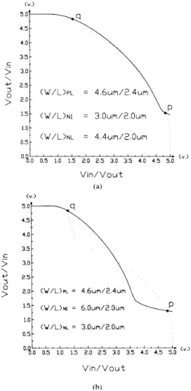
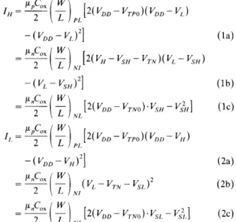
- - - - - ( W / L ) P L = 4.6um/2.4um (W/L)NI = 6,0um/2.0um . ( W / L ) N L = 3.0um/2.0um
-
-
’ VDD t I ( V . )\
4,6um/2.4um 3,0um/2,0um , (W”)N; , ,4,4Um/2 oU,Pl, , , ‘ 8 0 05 10 15 2 0 2 5 30 3 5 4 0 4 5 5 0 (’) V i n / V o u t (a)NTL circuits will be performed first. Then, the C, effect on the switching speed and performance evaluations for the NTL circuits will be discussed. Next, the principle of CNTL and its application will be described. Finally, exper- imental results will be shown to verify part of the theoreti- cal predictions.
11. BASIC ANALYSES OF CMOS NTL CIRCUITS
Fig. 2 shows the circuit configuration of a CMOS NTL NOR gate, which is employed as the basic building gate in CMOS NTL. The input signals are applied to the gates of parallel-connected NMOS transistors MNI’s. The PMOS M p L and the NMOS M N L serve as resistors to split the power supply voltage to reduce the output voltage swing. Nonetheless, the NMOS M N L introduces a negative feed- back effect, which will reduce the switching speed. In order to enhance the operational speed, a capacitor C, can be
shunted with M,, between node S and the ac ground
node to reduce this effect during switching. Because NOR is a complete logic function, the CMOS NTL circuit can have a straightforward logic construction style and is espe- cially suitable for design automation. It is also possible to obtain NAND structures in NTL forms by stacking several M,,’s. However, it will be shown later that since such NTL NAND circuits have no obvious speed advantages, they are not adopted as the basic NTL circuits.
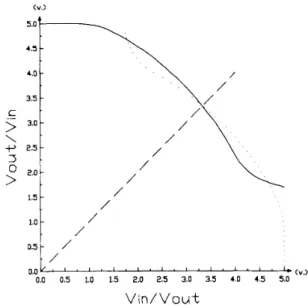
Typical dc voltage transfer characteristics of CMOS NTL inverters are shown in Fig. 3(a) and (b) for two different dimension designs. For the solid lines in these figures, the abscissa stands for the input voltage, and the ordinate for the output voltage, and vice versa for the dotted lines. As may be seen from these figures, the transfer curves are quite smooth. This implies no clear cut at the logic threshold. However. the two cross points p and q guarantee a correct logic operation. This is why the
WANG et ul.: CMOS NONTHRESHOLD LOGIC Cases MpL M N I M~~ 'H L' 'SH 'SL (,m) (pm) (pm) ( v ) ( v ) ( v ) ( v ) a 4.83 1.54 0.46 0.04 781 I H IL ( P A ) ( P A ) 333. 29.3 b -$&
%
4.69 1.78 0.81 0.12 325. 52.7 c dname nonthreshold logic is adopted. The output voltage swing of the NTL gate is designed to be about 3.5 V for a 5-V power supply, so that good noise immunity can still be retained.
It is seen that the transfer curves of Fig. 3(b) have larger open eyes than those of Fig. 3(a); thus the design of the former has higher noise immunity than that of the latter. Through several simulations, it is found that the dimension design of Fig. 3(b) for the CMOS NTL inverter is stable for a typical process fluctuation range in that there are always two cross points, p and q, in the transfer character- istics.
The first-order current equations are applied to analyze the dc characteristics of CMOS NTL gates and to obtain an approximate dimension design guideline. For a CMOS NTL inverter, the following equations can be obtained:
4.45 2.05 1.24 0.30 317. 90.6
%
4.83 1.30 0.85 0.07 339. 30.Cwhere I,,(,, is the dc gate current when the output voltage is low (high). Given ( W / L ) P l ~ , ( W / L ) , v l , and VI^, and making some approximations, the dc characteristics of the CMOS NTL inverter can be formulated. Detailed deriva- tions are performed in the Appendix.
Table I lists the SPICE-simulated dc characteristics of several CMOS NTL inverters with different dimension
ratios among MPL, M N , , and M N L . The transfer character- istics of Fig. 3(a) and (b) correspond to cases a and d , respectively, of Table I. The device parameters adopted in the simulations are of a 2-pm p-well CMOS process. AS compared with the SPICE simulation results, hand calcula- tions using the derived equations have an error within 20 percent if the mobility degradation due to the electric field is considered. Thus, these equations can be used as good design guidelines.
The CMOS NTL can receive the conventional CMOS signal directly, and vice versa. When a conventional CMOS gate comes after a CMOS NTL gate, the dimension design of the conventional CMOS gate is similar to the case where it is connected after a TTL gate, except that the logic transfer voltage should be adjusted to be equal to that of the NTL gate. On the other hand, because the voltage swing of a conventional CMOS gate fully covers that of a CMOS NTL gate, the CMOS NTL can then be connected immediately after the CMOS gate.
111. PERFORMANCE EVALUATIONS FOR CMOS NTL GATES
A . Speed and Power
Because the NMOS MNL results in a negative feedback effect, the switchng speed will degrade. By shunting MNI- with a capacitor C,, the negative feedback effect can be reduced during switching, and the speed is improved with- out an increment of power dissipation. To evaluate the extent of the improvement by increasing the value of C,, transient simulations on NTL inverters were performed. Since the characteristic waveform [15], [16] is the actual internal voltage waveform within an IC chip, it is more adequate to evaluate the speed performance from the characteristic waveform timing. To obtain the characteris- tic waveforms and their signal timing, a string of identical gates is excited and the output waveforms at the nodes of intermediate stages are observed. In the following descrip- tions, the average delay time of a gate is defined as half of the pair delay in the characteristic waveform case. For the characteristic timing, the average delay time of each stage gate is identical, and the delay time through N gates in series will be proportional to N [15], [16].
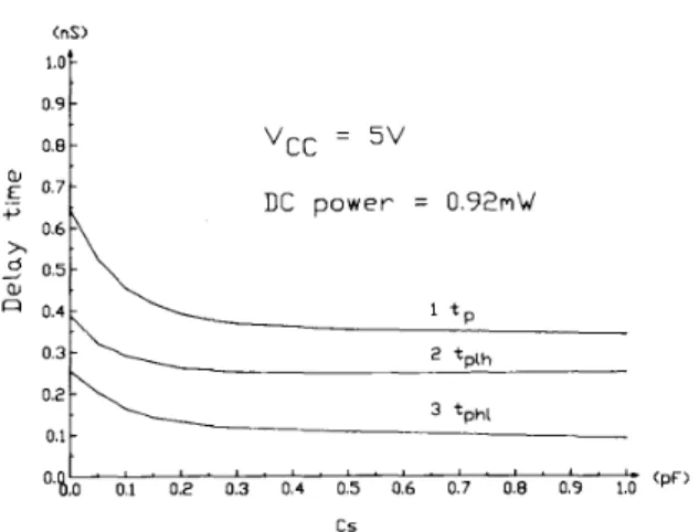
The simulated rise delay time t p l h , the fall delay time
t,,,, and the pair delay time t, versus the C, value are
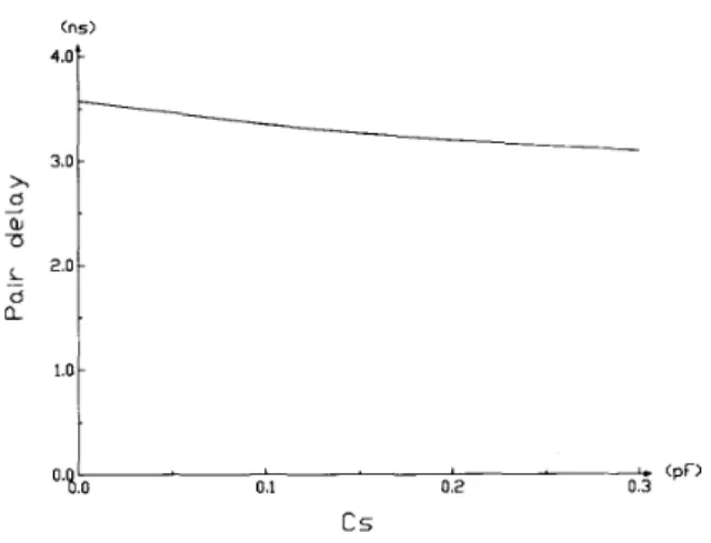
plotted in Fig. 4. The curves are monotonic decreasing. It is seen that the fall delay time t,,, is greatly improved by increasing the C, value slightly from zero because the main effect of Cy is to reduce the negative feedback effect on the series resistance in the discharging path from the output to the ground. On the other hand, the delay rise time t,,, is also improved because a faster falling input waveform results in a faster rising output waveform. All the improvements become saturated as the C, value in- creases further. It is found that a 0.2-0.25 pF C, is suitable for the 2-pm CMOS process.
1x2 I E E E J O ~ J R N A L OF SOLID-STATE CIRCUITS, VOL. 24, NO. 3, JUNE 1989
0.9 0.0
E"
0.7-CMOS NTL CIRCUITS WITH DIFFERENT FAN-OUT NUMBERS -
vcc
=s v
-
tphl 0.1 C S ( p F ) INa I N V d N O R Z d N O R 3 d NANDZd csFig. 4. The effect of reducing the switching delays by increasing the capacitance value of C' in a CMOS NTL gate.
N A N D 3 d 0 0 . 2 0 . 2 5 VDD f 0 . 7 2 0 . 7 6 0 . 5 2 0 . 4 4 1 . 0 3 1 . 2 5 0 . 6 1 0 . 4 6 0 . 3 1 0 . 2 6 0 . 7 3 1 . 0 6 0 . 5 9 0 . 4 4 0 . 2 9 0 . 2 4 0 . 6 9 1.00 I I I
Fig. 5. Circuit diagram of the CMOS NTL multi-input NOR gate. showing that the shunting capacitor C, is implemented by a MOS transistor.
From Fig. 4, it is seen that the speed of CMOS NTL is quite comparable to that of 12L [9] or even ECL
[lo].
Moreover, the minimum power-delay product of a CMOS NTL gate can be as small as 0.15 pJ for the 2-pm CMOS process. This value is smaller than the typical values of 1.0-1.8 pJ in ECL [lo] and 0.6-1.0 pJ in 12L [9] and is nearly the same as that of 1-pm standard CMOS logic [ll] under high-frequency operations. However, unlike the con- ventional CMOS logic, the CMOS NTL has dc power dissipation.By using the same CMOS device parameters, the SPICE-simulated delay times of CMOS NTL inverters, NOR gates, and NAND gates are shown in Table 11, where all the delay times are normalized to those of conventional CMOS inverters, NOR gates, and NAND gates, respectively. In this comparison, the device dimensions of conventional CMOS circuits are optimally designed so that in a CMOS inverter gate the ratio of the device dimension of the PMOS device to that of the NMOS device has a value near
,,'=
according to [12]. The inverters with a subscript a (or d ) in Table I1 denote that their device dimensions follow the design in case a (or d ) in Table I. For both types of NTL inverters with a C, of 0.25 pF, their delay times are found to be 0.59-0.44 times as small as those of conventional CMOS inverters. It is also found that the efficiency of C, in enhancing switchng speed in case d is hgher than that in case a. Besides this, the noise immunity of case d is better than that of case a , as described in the previous section; thus only case d is considered in simulat- ing NTL NOR and NAND gates. In Table 11, the numberafter the gate name denotes the fan-in number, e.g., the two-input NOR gate is denoted by NOR2. It is seen that the speed advantage can still be kept in NTL NOR gates. However, in multi-input NAND cases, NTL circuits do not have a better speed performance than the conventional CMOS NAND gates unless the shunted capacitance is larger than 0.25 pF. This is why only NOR gates are adopted as the basic gates in the developed CMOS nonthreshold logic. The fan-out effects of NTL gates are shown in Table 111. Here again, the delay times of NTL gates are normalized to those of CMOS gates. Because of smaller input capaci- tance, the speed advantage can also be found in multi- input, multi-fan-out NTL NOR gates.
B. C, Realization and Area Comparisons
Two problems are encountered in realizing the shunting capacitor C,. One is how to realize it; the other is the implementation area. The method to implement it is tech- nology dependent. In a single-metal p-well CMOS process, the method shown in Fig. 5 is found to be the most suitable. In Fig. 5, the CLy is implemented by a MOS transistor. The gate of the MOS transistor is connected to VDD, and its source and drain nodes are tied together and connected to node S in the NTL gate. A large voltage difference between the gate of the MOS transistor and node S makes the transistor work in the linear region to
provide a large gate-to-source/drain capacitance, and the very low node voltage swing at node S makes the capaci- tance stable. In the 2-pm CoMOS process, the nominal gate oxide thickness to, is 250 A, so an area of about 144 pm2 is needed to implement a 0.2-pF C,. It is expected that if an advanced technology such as the trench technology [ 131 can be used in realizing C.y, the area needed can be greatly
WANG et ul. : CMOS NONTHRESHOLD LOGIC 7 x 3
logic
g a t e s
i1
- m e t a lINV NOR2 NOR3 NOR4
c o n t a c t
C M O S
Fig. 6. Layout diagram of a CMOS N T L inverter using 2-pm design rules.
1.00 1.00 1.00 1.00
TABLE IV
NORMALIZED LAYOUT AREAS OF CONVENTIONAL CMOS AND
CMOS NTL GATES
I I I I I
I
NTL
I
1.91 1.04 0.81 0.69reduced. A layout diagram of an NTL inverter using 2-pm single-metal CMOS design rules with the C, realized by a MOSFET is given in Fig. 6.
Based upon the same design rules, layout diagrams of various conventional CMOS gates and CMOS NTL gates with C, equal to 0.25 p F were generated. Layout-area comparisons are shown in Table IV, where the area of each conventional CMOS gate is normalized to unity. It is seen from this table that the layout area of an NTL inverter gate is really larger than that of a conventional CMOS inverter because of the extra area needed for C,. However, for all gates more complex than a two-input NOR gate, the areas of the NTL gates become compatible to or even less than those of the corresponding conventional CMOS gates, due to the redundant device usage in conventional CMOS gates. Therefore it is realized that the extra area needed for C, is tolerable for those complex gates.
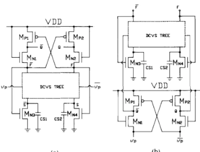
From the results in the previous sections, we have seen that CMOS NTL circuits can have a very high speed performance. They are therefore especially suitable for applications requiring high speed. The penalty paid is the high static power consumption. In some applications, there can be a trade-off between speed and power. To achieve such a trade-off, another logic circuit, called the CMOS cascode nonthreshold logic (CNTL) circuit, is developed. The basic idea in implementing the logic is to apply the nonthreshold logic to the recently developed cascode struc- tures [1]-[3] where complex cascoded A01 circuits are permitted.
Vpv DCVS TREE
. J
VDDJ .
T T
lab (b)
Fig. 7. (a) The basic CNTL circuit and (b) a reconfigurated C M O S C N T L gate.
The CNTL principle is shown in Fig. 7(a), and the basic CNTL gate can be reconfigured as in Fig. 7(b), just as the DSL circuit [3]. The circuit structure is similar to the differential split-level logic (DSL), but the electrical behav- ior is essentially different. Like all cascode logic circuits, the CNTL has a differential cascode voltage switch (DCVS) tree [l], [3] constructed by NMOS devices. Similar to the DSL circuit, two cross-coupled PMOS devices are used as loads, and two NMOS devices, M N 1 and M N 2 , are inserted between the PMOS loads and the NMOS logic tree to split the supply voltage to reduce the output voltage swing. However, the gates of the two NMOS devices M,, and M N 2 are connected together to VDD, not to a reference voltage
yef
as in the DSL circuits. So the voltage reference circuit and the routing area needed foryef
are eliminated. Q and0
are two true output nodes, and F andF
are two pseudo-output nodes which have smaller voltage swings and can be used for wire routing among different gates as in the DSL circuit. The main difference between the CMOS CNTL and the DSL circuit is that the two NMOS devices, M N 3 and M N 4 , and the two shunting capacitors, C,, andCs2, are added below the DCVS tree to form the non- threshold circuit. The shunting capacitors can be imple- mented by using MOS transistors as in the NTL case. Unlike the basic NTL circuit, whch connects the gate terminal of M N L to VDD, the gate terminals of M N 3 and MN4 in the CNTL gate are connected to the nodes F and
F,
respectively, to make the layout of Fig. 7(b) more compact. It is found that this connection does not affect the negative feedback effects of M N 3 and M,. As ex- pected, the NMOS M N 3 and MN4 can further reduce the output voltage swing, and their negative feedback effects can be reduced by C,, and Cs2.The DCVS trees for the sum and carry outputs of a CNTL full adder are shown in Fig. 8. The device dimen- sions of the MOS’s, M p l . M p z , M,Y1, M,%,, Mhr3, and M , , , and the simulated dc characteristics are shown in Table V. As shown in this table, the output voltage swings at the nodes Q and
Q
of the CNTL gate are about from 1.5 to784
4.83
IELE JOURNAL OF SOLID-STATE CIRCIJITS, VOL. 24, NO. 3, JIJNE 1989
1.50 1.3-3.0 0.0-0.9 139 72
S S C. C O
P
Delay (ns)
per ( p J )
Fig. 8. The DCVS trees required to implement the sum and carry functions of a full adder.
2.5 2.0 1.2 1.7
0.8 4.6 9.7 2.2
TABLE V
SIMULATED DC CHARACTERISTICS OF A CMOS CNTL FULL ADDER
TABLE VI
PERFORMANCE COMPARISONS OF THE SUM CIRCUITS OF THE FULL ADDERS IMPLEMENTED BY THE CONVENTIONAL CMOS, THE DSL.
THE NTL. AND THE CNTL CIRCUITS
3
1
P o w e r ( m W )
4.8 V, and those at the nodes F and
F
are about from 1.3 to 3.0 V. Just as with the DSL gates, the nodes E andF
with smaller voltage swings can be used for connection among different gates. Because the maximum voltage drop between the drain and source nodes of all PMOS and NMOS devices is below 3.5 V, for the same processing technology shorter channel length can be used in CNTL gates than in other types of logic gates to improve the switching speed without serious hot carrier effects [3], [14].Due to the lower voltage swings at the output nodes F and
F,
and the nonthreshold technique applied, the speed of the CNTL circuit is expected to be faster than that of the DSL circuits under the same power consumption.The SPICE-simulated transient results at the sum cir- cuits of the full adders implemented by conventional static CMOS, DSL, NTL, and CNTL are compared in Table VI with all Cs’s = 0.25 p F in CMOS NTL and CNTL gates. The sum circuit implemented by the CMOS NTL is a three-level logic circuit. From Table VI, the speed of the CMOS NTL adder is seen to be the fastest of all the
Ir!
1. <pF)O.t!o
0.1 0.2 0.3c s
of the CMOS CNTL gate.
Fig. 9. The effect of an increasing
c,
value on the speed performanceimplemented adders, and that of the conventional CMOS adder is the slowest. The speed of the CNTL adder, although slower than that of the NTL adder, is still higher than that of the DSL adder. Moreover, the power dissipa- tion of the CNTL circuit is nearly half that of the DSL circuit. Thus, the CNTL circuit has a smaller power-delay product than the DSL circuit.
It can be seen from Table VI that the NTL circuit is faster than the CNTL circuit. However, the CNTL circuit has a much smaller dc power dissipation due to the use of the cross-coupled loads and the complex cascode A01 circuits. Generally, the NTL circuits and the CNTL cir- cuits have different features to meet different requirements or specifications.
The C, effect on the speed of CNTL gates is shown in Fig. 9. The shunting capacitor can also reduce the negative feedback effect and improve the speed. However, its effect is not so significant as in NTL gates because of the NAND/AND circuit structure used in CNTL gates. A capac- itance value of 0.2-0.25 pF is selected for the 2-pm CMOS technology as in the NTL gates.
V. EXPERIMENTAL RESULTS
Some experiments were performed to verify part of the simulated results. Several strings of 71-stage ring oscilla- tors were designed and fabricated to measure the average delay time of NTL inverters and two-input NTL NOR gates using a standard 2-pm single-metal p-well CMOS process. For comparisons, similar test structures were also designed and fabricated for conventional CMOS inverters and two- input NOR gates. The C, values in the fabricated NTL gates are all chosen to be 0.25 pF. A chip photomicrograph is shown in Fig. 10. The measured dc transfer characteris- tic of the fabricated NTL inverter is shown in Fig. 11, which is very close to the simulation results. The measured output waveforms of the fabricated ring oscillators with two-input NTL NOR gates are shown in Fig. 12, and the measured timing data are listed in Table VII. It is seen
WANG et d. : CMOS NONTHRESHOLD LOGIC 7x5 4.0 3.5 c .
__
>
3.0 \ .+
2.5Fig. 10. Photomicrograph of the fabricated ring oscillators made of CMOS NTL inverters or NOR gates.
-
-
--
(V.) 4.55'0h
\
/ / / / 0.5 0.0 l ' O 1 0.0 0.5 1.0 1.5 2.0 2.5 3.0 3.5 4 0 4.5 5.0 V i n / V o u t (V.)Fig. 11. The measured dc transfer characteristics of the fabricated CMOS NTL invertcr.
TABLE VI1
M ~ A S ~ I R E D D t l A I TNLS Ot FABRICATLD C O N \ t U l l O h A I CMOS GATIS A N I ) OF CMOS NTL G A I ~ S FOR CO\IPAKISOL
G a t e s
Performance
NTL/CMOS
that the measured delay time of the NTL inverter is about one-third that of the conventional CMOS inverter, and the delay time of the NTL NOR gate is about one-fourth that of the conventional CMOS NOR gate. These experimental observations are all consistent with the theoretical predic- tions described in Section 111.
VI. CONCLUSIONS
In this paper, two novel static CMOS logic circuits are proposed, analyzed, and partly chip-tested. First, the CMOS nonthreshold logic (CMOS NTL) is shown to be the fastest logic of the various static CMOS logic circuits. It has a simple logic construction style. The other new CMOS logic. the CMOS cascode nonthreshold logic (CMOS CNTL), is also shown to have a high speed performance. I t offers a suitable trade-off between the high speed characteristics of the NTL circuits and the low power characteristics of the cascode CMOS circuits. We believe that these two new hgh-speed logic circuits will extend the application regime of digital CMOS IC's.
APPENDIX
Given K p , . K,,, and V,, K , , , VI,. V y H . and Vsr can be solved from the dc current equations in (1) and (2). Mak- ing a reasonable assumption that ( VDD - + 0 in (2). then
Substituting ( A l ) into (1) and solving for I,, and I , . we have
From (2) and (A3), we have
(A41 Fig 12. The measured output waveform of the fabricated ring oscillator
7x6 0, K , , can be solved as (A51 I L
2v,,(
Vnn - VT,1
‘ K , , =Then, substituting ( A 2 ) and (A5) into
(IC)
and solving for V71i, we haveREFERENCES
L. G. Heller. J. W. Davis. and N. C;. Thoma, “Cascode voltage switch logic: A differential CMOS logic family.” in ISSCC Dig
Tech. Pupers. Feb. 1984, pp. 16-17.
C. K. Erdelyi, W. R. Griffin, and R. D Kilmoyer. “Cascode voltage switch logic design,” VLSI Design, pp. 78-86. Oct. 1984. L. C. M. G. Pfennings. W . G. J. Mol, J. J. J. Bastiaens. and J M. F. V. Dijk, “Differential split-level CMOS logic for subnanosecond speeds,” IEEE J . Solid-Sure Circuirs. vol. SC-20. pp. 1050-1055. Oct. 1985.
R. H. Krambeck. C. M. Lee, and H. S. Law, “High-speed compact circuits with CMOS,” IEEE J . Solid-Stute Circuirs, vol. SC-17. pp.
614-619, June 19x2.
N. F. Goncalves, and H. J. De Man, “NORA: A racefree dynamic CMOS circuit technique for pipelined logic structures,” I )
Solid-Store Circuits, vol. SC-18. pp. 261-266. June 19x3. K. M. Chu. and D. L. Pulfrey, “ A comparison of CMOS circuit techniques: Differential cascode voltage switch logic versus conven- tional logic,” IEEE J . Solid-Stufe Circuits, vol. SC-22, pp. 528-532.
Aug. 1987.
H. M u k a , T. Sudo, and H. Kindo. “NTL-LSI circuit design consideration,’’ Rei). Elec. Cornniun. IA/J , vol. 21. pp. 541-546. Sep t . - Oct. 1 973.
R. Ranfft and H.-M. Rein. “High-speed bipolar logic circui low power consumption for VLSI-A comparison.” IF Solid-Stute Circuits, vol. SC-17. pp. 703-712. Aug. 1982. S. K. Wiedmann, “Advancements in bipolar VLSI circuits and technologies.” I E E E J . Solid-Store Circuits, vol. SC-19. pp. 282-291. June 1084.
S. Tanaka et al.. “A subnanosecond XK-gate CMOS/SOS gate array,” I E E E J . Solid-Sture Circuirs. vol. SC-17. pp. 614-619. June 1982.
T. Yamaguchi, S. Morimoto. G. H. Kawamoto. and J. C. Delac!. “Process and device performance of 1 pm-channel n-well CMOS technology,” IEEE J . Solid-Stute Circutr.\. vol. SC-I 9. pp. 71-XO. Feb. 19x4.
A. Kanuma. “CMOS circuit optimization.” Solid-Srure Elrct~oii , vol 26, no. 1, pp. 47-58. 1983.
A. Shah et ul.. “A 4 Mbit DRAM with trench transistor cell.” J . Solid-Store Circuifs, vol. SC-21. pp. 61X-626. 19x6. , S. C. Tam, F.-C. Hsu, P.-K KO. T.-Y. Chan. and K. W. Tcrrill. “ H o t electron-induced MOSFET degradation- Model. monitor, and improvement,” IEEE T r u m Electron D r v i t e ~ . \ o l ED-32, pp. 375-385. Feb. 19x5
C.-Y. Wu, J.-S. Hwang, C. Chang, and C.-C. Chang. “ timing model for CMOS combinational logic gates.” I
Conipurrr-Aided Design, vol. CAD-4. pp. 636-650. Oct. I985 C.-Y. W u and T.-S. Wu. “A new physical timing model for bipolar NTL circuits.” in Proc. I988 Bipolur Circ.uit\ Tec.Iiiio1. ,tfeetiii,y,
Sept. 19x8. pp. 223-226.
,linn-Sh\an b a n g (S‘h?-V’XX) \\a\ born in Yucii-Lin Tai\\an Republic of China. in 1959 He recei\ed the H S degree i n electrical cnginccr- ing from the Xational (heng-Kting UniiCJ\lt\ i n 19x2 m d thc M S and Ph D degree\ from the In\titutc of Electronic\ \ation,il C h i a ~ - T ~ i t i g Uni\cr\it\ Tainan. in 19x4 and IYhX rc,pci- ti\eI\ He wa\ awarded the 1 Y X X Long-Tung The\(\ Auard from Sertck International lnc Tala an
He I \ no\\ \\it11 the Eleitronic\ Re\carch b Senice Orgmization. Industri‘il Technolog\ Re\earch In\titutc Tai\\an engaged in the delclopment of digital T\ chip \ e t \ Hi\ main tewarch intcre\t\ are digital high-\peed integrated circuit dc\ign and digital \ignal proce\\ing
Chung-ku h u (S‘7i-hI‘77) \\a\ horn in C h i r i \ i Taiwan. Republic of China o n \ l d \ 31 1Y50 He recei\ed the 13 S dcgrec from the Department of Elcctroph\\ic\ and the M S and Ph D degree\ from the In\titutc of Electronic\ at the Uational Chiao-Tung Uni\cr\it\. H w x h u T‘iiaan Rc- publlc of China in 1972 1976 and 19XO rc\pcc- t l \ C l \
In 1975 and 1976 he \tuciicd fcrroelectrii film, o n \ilicnn and their dc\icc
the \ear\ 1976-197’) he en nient of integritcd differential negati\e re\i\t,in
circuit applications. a i t h \upport from the h,iticinil Flectronic\ \ l a \ \
Plan (Semiconductor Dc\ice\ and Integrated Circuit Technologies) of the National Science Council From 19x0 to 19x4 he \ \ a \ a n A\\oiiatc Profe\\or at the In\titute of Electronic\. hational Chiao-Tung Uni\er\it\ During the \car\ 19x441086 he \ \ a \ an A \ \ O L I J ~ C Profe\\or i n thc Department of Electrical Engineering Portland State Uni\cr\it\ Port land. OR Pre\entl\ he i \ Profe\\or in the Department of Elcctronii\ Engineering and the In\titute of Electronic\ r\,itional Chiao Tune, Uni \ersit\ Hi\ rcwirch intere\t\ h a \ e been in dc\icc modeling. integr‘itcd- circuit tcchnologie~. \cmiconductor nicniorie\ analog integrated c1rcLii[\ digital inteerated circuit\. and computer-aided ciicuit de,ign
member of Eta Kappa \ U and Phi TJLI Phi Dr W u I \
Ming-Kai Twi ( M ’ X 2 ) \\a\ born in Ping-Tung. Taiwan. Republic of China. in lY50. Hc rcxi\cd t h e B S degree in electrical engineering froin National Taiaan Uni\crGt\. Taipci. T.ii\\an. i n 1971 and the 41 S. degree i n electrical ciigi- nccring from thc Uni\crsit\ of Cincinnati. Cincinnati. OH. in 1976.
During the \car\ 1976-19X.7 he \\a\ w i t h the Electronic Rcwarch and Sen i c c Organijation. Indurtriril Technolog! Rcwarch Institute (ERSO. ITRI). Tainan. Lvlicrc he \\ah initiall\ iiii MOS
IC Design Engineer. He bccamc thc Manager of the Microcompiitcr IC I h i g n Department i n 19x0 Sincc 19x3 he has been Director .>f the Rocarch and De\elopment Dcpartmcnt Lit the United .Ilicroslcctronic~ Corporation. Hsin-Chu. Tain a n . rcrpon.\iblc for a11 research and dciclop- iiicnt \\ark on MOS VLSI circuit and \\htcni dcrign