transient mechanisms are proposed in this paper. The bidirectional current mode capacitor multiplier technique can effectively move the crossover frequency toward to the origin in the start-up pe-riod for a smoothly rising of the output voltage. Besides, the small time constant is set by the fast transient control circuit in order to get a higher crossover frequency. Thus, the output voltage can be regulated to its stable value as fast as it can when large load cur-rent changes. A test chip fabricated by the Taiwan Semiconductor Manufacturing Corporation (TSMC) 0.35- m process verifies the correctness of the bidirectional current mode capacitor multiplier technique. Experimental results demonstrate the transient speed by our proposed technique is faster than that by conventional con-trol by about 2 times, and there is only about 76% dropout voltage of the conventional design with off-chip compensation. The pro-posed circuits consume more quiescent current about 10 A in single-ended capacitor multiplier and 20 A in two-ended capac-itor multiplier. With the proposed bidirectional current mode ca-pacitor multiplier technique, the performance of dc-dc converters is improved significantly and the external pins and footprint area are minimized.
Index Terms—Capacitor multiplier, compensator, current mode,
dc-dc converter, on-chip compensation.
I. INTRODUCTION
P
ALM-sized devices like cellular phones, personal digital assistants, digital cameras, music players, and other multi-media entertainments demand highly integrated circuits. Higher level of integration yields better performance resulted from a reduction of parasitic components of bonding wires, connec-tions, or package. Unfortunately, off-chip inductors and capac-itors take up significant area on PCBs, add production cost, and obstruct system-on-chip (SoC) applications. For the sake of re-ducing harmful effects of bonding wire parasitic elements and power loss on them, making all the circuits to be on-chip be-comes a matter of concern. High integration is necessary for Manuscript received August 24, 2006; revised June 25, 2007. This research is also supported by the National Science Council, Taiwan, R.O.C. under Grant NSC 96-2221-E-009-240. Recommended for publication by Associate Editor E. Santi.K.-H. Chen is with the Department of Electrical and Control Engineering, National Chiao Tung University, Hsinchu 30010, Taiwan, R.O.C. (e-mail: khchen@cn.nctu.edu.tw).
C.-J. Chang was with the Department of Electrical and Control Engineering, National Chiao Tung University, Hsinchu 30010, Taiwan, R.O.C. He is now with EMP, Inc., Taiwan, R.O.C.
T.-H. Liu Department of Electrical and Control Engineering, National Chiao Tung University, Hsinchu 30010, Taiwan, R.O.C. He is now with Novatek Cor-poration, Hsinchu, Taiwan, R.O.C.
Color versions of one or more of the figures in this paper are available online at http://ieeexplore.ieee.org.
Digital Object Identifier 10.1109/TPEL.2007.911776
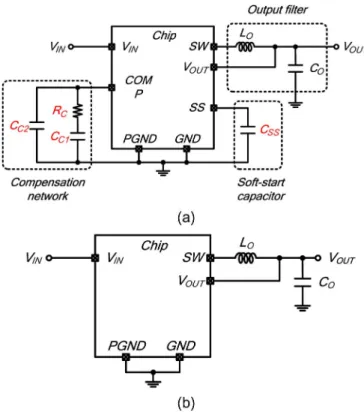
Fig. 1. (a) Typical application circuit for dc/dc buck converter with current mode control. (b) Proposed dc/dc buck converter with minimized external pins and components
achieving high performance and small footprint area in portable equipments today.
As we know, it is imperative to integrate large off-chip com-pensation and soft-start capacitors in Fig. 1 into the chip for min-imizing external pins and footprint area. In Fig. 1, the conven-tional compensation network contains a resistor and capaci-tors and ; the soft-start mechanism contains a capacitor . Thus, after the integration of these passive components, the chip can have minimized external pins and need only the output filter, which contains an inductor and a capacitor . If the integration of the output filter into the chip is needed, the technique of system-in-package (SIP) can be used to implement the large off-chip output filter [1], [2].
Thus, for low cost and high integration, a bidirectional cur-rent mode capacitor multiplier technique to implement a buck converter with minimized external pins and high performance is proposed. In other words, the functions of compensation, soft-start, and fast transient response are achieved by the proposed bidirectional current mode capacitor multiplier technique at the same time. It means that only a low-cost and bidirectional cur-rent mode capacitor multiplier technique is used to eliminate the 0885-8993/$25.00 © 2007 IEEE
Fig. 2. Current-mode dc-dc converter with the proposed bidirectional current mode capacitor multiplier technique.
demand of external pins ( and ). Besides, owing to the bidirectional current mode capacitor multiplier technique, the output overshoot/undershoot voltage in case of load varia-tions is smaller than that of conventional design.
The difficulty of high integration in the design of dc-dc con-verters is due to the large off-chip capacitors of proportional integration (PI) compensation and soft-start function. PI com-pensation technique [3]–[6] achieves a popular pole-zero can-cellation for compensating current mode buck dc-dc converters. The compensator must generate a pair of pole-zero to coun-teract the dominant pole and form a new suitable dominant pole for the designed bandwidth. However, large-valued capacitors needed for compensation often occupy substantial space. Thus, in order to not occupy large silicon area, the high integration is achieved by modifying the time constant. Under the deliberate control procedure of error amplifier, the response of error ampli-fier is increased in case of large load variations and decreased in case of start-up process. At normal operation, the control circuit works as a current mode Miller multiplier for achieving large on-chip capacitance in order to implementing lag compensation (PI compensation). It means that minimizing the size of capac-itors can alleviate the tradeoff between cost and performance thereby maximizing profit.
The bidirectional current mode capacitor multiplier technique contains the functions of on-chip compensation, soft-start, and fast transient response is proposed in this paper. The circuit anal-ysis and implementation is proposed in Section II. Importantly, in order to improve the performance of the dc-dc converters, the time constant is adaptively modified for dynamically changing the crossover frequency. Smooth soft-start period and fast tran-sient recovery are achieved by the single-ended bidirectional capacitor multiplier technique. In Section III, the concept of the single-ended capacitor multiplier technique is extended to two-ended technique for the implementation of type II compen-sator. The test chip is fabricated by TSMC 0.35 m process and experimental results are shown in Section IV. Finally, a conclu-sion is made in Section V.
II. SINGLE-ENDED BIDIRECTIONALCURRENTMODE CAPACITORMULITPLIERTECHNIQUE
The single-ended bidirectional current mode capacitor multi-plier technique is shown in Fig. 2. Observe that the bidirectional
Fig. 3. Capacitor multiplier techniques. (a) Voltage mode. (b) Current mode.
current mode capacitor multiplier circuit implements the func-tions of compensation, soft-start procedure, and fast transient response. In the presence of the bidirectional current mode ca-pacitor multiplier circuit, the external components that contain
output filter ) and feedback resistors are
mini-mized owing to the on-chip compensation and soft-start capaci-tors. Thus, the low-cost buck converter with minimized external pins is achieved by the proposed technique. The output of our proposed buck converter output contains only an output filter . It means that the converter needs a small footprint area and, correspondingly, a low cost.
A. Voltage-Mode and Current-Mode Miller Capacitances
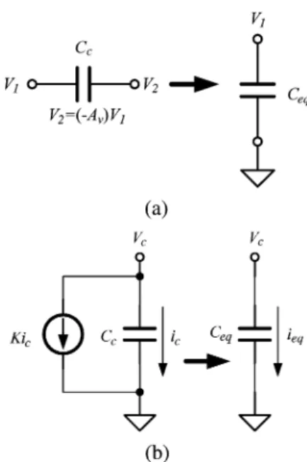
Generally speaking, there are two techniques [7] to get an equivalent capacitor, one technique is so-called voltage-mode and the other is current-mode. Based on the Miller theorem, the equivalent capacitor is equal to the original value multiplied by a factor if the voltage of one terminal of the capacitor is times that of the other terminal as shown in Fig. 3(a). The equivalent value of capacitor is as
(1) The other popular current-mode technique of capacitor mul-tipliers is shown in Fig. 3(b). The concept is to sense the cur-rent through a small capacitor, then amplify and bypass this am-plified current across the two terminals of the small capacitor. Therefore, the equivalent capacitor is derived by the following equations:
(2) Several capacitor multiplier circuits have been proposed [7]–[11]. There is a voltage-mode Miller capacitor multiplier applied in phase-locked loops needs a negative gain amplifier
plier circuit.
[11]. Besides, the amplifier must have no input dc current because such a dc current results in large leakage and voltage spur. Therefore, a noninverting amplifier followed by a neg-ative unity gain buffer is necessary, although there is still a leakage current flowing through feedback resistors. However, one important design restriction is that large multiplication factor may induce severe gain compression. Because when the input of operational amplifier experiences large voltage swing, its output voltage is limited by power rails. Consider a current-mode capacitor multiplier [7] used in a single-stage amplifier that is used an output stage of operational amplifier. Traditional Miller compensation could be accomplished by this multiplied capacitor. However, current mirrors can only amplify one direction of the current flowing through the small capacitor, so extra dc bias currents are necessary for this tech-nique. The summary is that the capacitor multiplier is needed to have the characteristics, which are no dc current consumption, large signal swings, and little silicon area.
B. Analysis of the Single-Ended Capacitor Multiplier for On-Chip Compensation, Soft-Start, and Fast Transient Operations
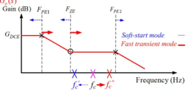
Fig. 4 shows the frequency response of the bidirectional current mode capacitor multiplier technique. The plot is similar to the lag compensation with a higher frequency pole for alleviating the high noise effect. Thus, it contains two poles and one zero [3], [4]. It is interesting and useful to observe that the effective crossover frequency different from that of normal operation at start-up and fast transient operation. As we know, the crossover frequency should be extended to a higher frequency at fast transient operation. However, it should to be moved to a lower frequency at start-up operation. In other words, the bidirectional current mode capacitor multiplier circuit modifies the positions of two poles and one zero to a suitable frequency positions. In the meanwhile, the operation of the proposed bidirectional current mode capacitor multiplier technique makes sure the stability of the system.
Fig. 5 illustrates the symbolic description of the proposed bidirectional current mode capacitor multiplier circuit. The dy-namic current source is to generate an equivalent current whose value is times the current flowing through the compen-sation capacitor . It means that the equivalent series
capac-Fig. 5. Symbolic description of the proposed time constant technique.
itance is increased to be large enough to generate a low-fre-quency pole-zero pair and . For the soft-start opera-tion, the equivalent capacitance is larger than that at the normal operation. Besides, the value of is smaller than that of the normal operation for a large separation between the pole and the zero . In fact the effective crossover frequency is close to the origin for achieving a lower bandwidth. Large time constant makes sure the smooth increase in the output voltage of the error amplifier. Therefore, the soft-start function can pre-vent the output voltage from overshooting by such a large time constant.
Contrarily, small time constant increases the response of the error amplifier in case of load variations. Thus, the bidirec-tional current mode capacitor multiplier technique decreases the equivalent capacitance in order to move the pole-zero pair to higher frequency as shown in Fig. 4. In the meanwhile, the ef-fective crossover frequency is moved to a higher frequency to get a large bandwidth. However, the utmost importance that we should watch out for is the stability of the system. Thus, the large bandwidth with small phase margin lasts for a short pe-riod and the crossover frequency comes back the original value at the normal operation. Fast transient response is achieved by a small time constant and the stability is assured by the control of large time constant period [12], [13].
The single-ended bidirectional current mode capacitor mul-tiplier technique makes sure the smooth operation of soft-start and the fast transient response in case of load variations. The following subsections describe the implementation of the pro-posed single-ended bidirectional current mode capacitor multi-plier technique.
C. Implementation of the Single-Ended Capacitor Multiplier
The implementation of the adaptive capacitance is shown in Fig. 6(a). Two transistors, and , biased in triode region works as two resistances and . The ratio that is the as-pect ratio of transistor is divided by that of transistor is . It means that the current flowing through the transistor
is times that of transistor . Thus, an equivalent ca-pacitance is got by the value of the capacitor multiplied by . The equivalent small-signal model is shown in Fig. 6(b). and are the open-loop output resistance and transcon-ductance of the voltage follower [14], [15], respectively. The voltage follower implementation is shown in Fig. 6(c) [15]. Ac-cording to the analysis of literature [16], the transfer function
Fig. 6. Implementation of an adaptive capacitance circuit for achieving a vari-able capacitance at different operation modes. (a) The design of circuit. (b) The small-signal model of the circuit. (c) The schematic of the voltage follower used in the capacitor multiplier.
and the current ratio are described as (3) and (4), respectively,
(3)
(4)
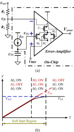
Fig. 7. Conventional soft-start circuit of dc/dc converters. (a) The circuit im-plementation. (b) The operation regions of the three input transistors in the mod-ified amplifier for soft-start.
If and , (3) and (4) are approximated
as (5) and (6), respectively,
(5) (6) Thus, the equivalent input impendence for capacitor multi-plier can also be approximated as
(7)
The equivalent input resistance generates a low-fre-quency pole-zero pair. However, if the resistance is too small, the approximation is not valid. Hence, an offset value exists in the capacitor multiplier and may cause the capacitor multiplier mechanism inaccurate.
D. Implementation of the Soft Start in the Bidirectional Current Mode Capacitor Multiplier Technique
The conventional soft-start circuit is shown in Fig. 7(a) [4]. The large soft-start capacitor and the small bias current make sure the voltage smoothly ramps up the output voltage. Thus, the transistor is added to the input differen-tial stage of error amplifier to substitute for the role of reference
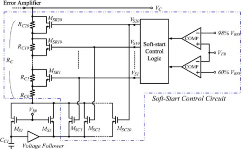
Fig. 8. Proposed bidirectional current mode capacitor multiplier technique with the function of soft-start.
Fig. 9. Soft-start control logic in the proposed bidirectional current mode ca-pacitor multiplier circuit.
is off and the transistors and comprise the differen-tial input pair; hence, the error amplifier regulates to .
When approaches , transistor starts to conduct,
and transistor turns off gradually. Once is high enough, the transistor is completely turned off, and transistors and then regulate to . The operation regions of the three input transistors are shown in Fig. 7(b). However, the tran-sition from soft start period to normal operation is not smooth in conventional design because there are two control signals and are compared to the feedback voltage . Thus, an overshoot is observed in conventional design. It is of utmost im-portance to get a large time constant for implementing the func-tion of soft start.
In order to implement the function of soft-start, the bidirec-tion current mode capacitor multiplier circuit is modified as Fig. 8. The resistor in Fig. 5 is divided into small resistors , and its value is determined by the aspect ratio
of transistors . Hence, the more the switches
are turned on, the smaller the value of . Besides, the equiv-alent capacitance is also increased by turning on the switches to decrease the value of time constant.
Be-cause the separation of the pole-zero pair is needed, all the switches are turned on at the beginning of start-up period. It promises the effective crossover frequency is located at a lower frequency than that at normal operation. When the feedback voltage is larger than 98% , the soft-start control logic generates a sequence of pulses to turn off the switches
and in sequence to
re-turn the value of time constant back to that at normal operation. Owing to the small time constant, the smooth increase of the output voltage is achieved by the modified time constant circuit in Fig. 8.
Fig. 9 illustrates the soft-start control logic circuit. Two comparators are used to determine the start and stop points of soft-start mechanism. One comparator compares the feedback
voltage with 60% to decide the start point of soft
start function. The time constant is increased to a large value to get a smaller crossover frequency in Fig. 4. Furthermore, it maintains this large time constant until the feedback voltage is larger than 98% . Then, the second comparator sends logic high to SR latch to start the pulse sequence circuit. The pulse sequence circuit provides a smooth transition from soft start operation to the normal pulse width modulation operation. In other words, the crossover frequency at soft start operation is moved back to at the normal operation. The pulse sequence circuit is enabled by the output SR-latch and generates a carry out to trigger the shift register. Thus, the shift register sets the values of from high to low in sequence for decreasing time constant. In the meanwhile, the crossover frequency is smoothly moved back to the value of at the normal operation. Owing to the smooth transition of crossover frequency, the overshoot of the output voltage can be alleviated. In other words, the bidirectional current mode capacitor multiplier technique with soft-start mechanism can effectively alleviate the inrush current of the inductor.
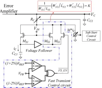
E. Fast Transient Mechanism in the Bidirectional Current Mode Capacitor Multiplier Technique
Contrarily, the time constant is needed to be decreased when load changes. A small time constant moves the crossover
fre-Fig. 10. Proposed bidirectional current mode capacitor multiplier technique with fast transient mechanism.
quency to a higher frequency for achieving a fast transient response [12], [13]. However, what we need to take care is the stability of the system because of the higher crossover frequency has less phase margin. Thus, two comparators are used to detect the start time of the fast transient function and prevent the output voltage from ringing. The fast transient mechanism is stopped when the difference between the feedback voltage and the
reference voltage is within 2% . Once the output
voltage drops lower than about 2% or rises higher than above 2%, the fast transient circuit starts to decrease the time constant. The equivalent resistance in Fig. 6(b) gener-ated by the transistor is divided into two small transistors and in Fig. 10. Besides, the sum of the two aspect ra-tios of transistors and is equal to that of the original transistor in Fig. 6(a). The gate of transistor is set to low when the fast transient function starts in order to get a small equivalent capacitance. Then, the system has a wider bandwidth in Fig. 4 to get a fast response. The phase margin of this fast transient operation is kept larger 45 in order to make sure the stable regulation of output voltage.
III. TWO-ENDEDBIDIRECTIONALCURRENT-MODE CAPACITORMULTIPLIERTECHNIQUE
Owing to the previous analysis of the single-ended bidi-rectional current mode capacitor multiplier technique, the concept can be extended to the two-ended capacitor multiplier technique.
A. Two-Ended Capacitor Multiplier in Type II Compensator
Fundamental type II compensator is composed of an error
amplifier, two resistors and two capacitors as
Fig. 11. Typical type II compensator.
Fig. 12. (a) Proposed architecture of two-ended capacitor multiplier within type II compensator. (b) Equivalent circuit of proposed two-ended bidirectional capacitor multiplier within type II compensator.
shown in Fig. 11. The transfer function of the fundamental type II compensator is given by (8). Replacing this fundamental type II compensator by the proposed two-ended capacitor multiplier is shown in Fig. 12(a). The similar operation of both terminals is that the small signal current flowing through both sides of small capacitor is multiplied by the same amplification factor . Therefore, capacitor could be replaced by the small capacitor and proposed two-ended bidirectional capacitor multi-plier. The equivalent circuit of proposed two-ended capacitor multiplier within type II compensator is shown in Fig. 12(b). The voltage follower is also modeled to have a single-pole response. The transfer function of the implementation circuit in Fig. 12(b) is derived as (9) at the bottom of the page.
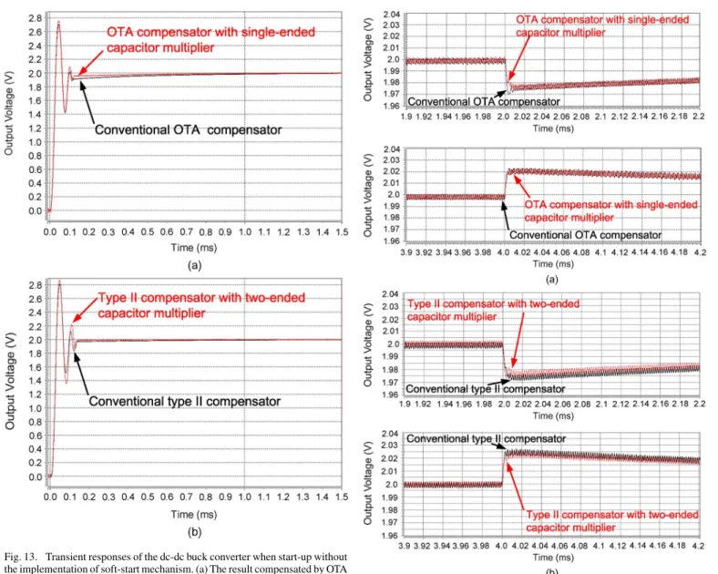
Fig. 13. Transient responses of the dc-dc buck converter when start-up without the implementation of soft-start mechanism. (a) The result compensated by OTA compensator with the single-ended capacitor multiplier and that with conven-tional off-chip compensation. (b) The result compensated by type II compen-sator with the two-ended capacitor multiplier and that with conventional off-chip compensation.
The voltage follower implementation is shown in Fig. 6(c) [15]
(8)
and in (9) where and are the dominant pole and dc
transconductance at the first stage of the voltage follower, re-spectively. and are the components of Miller compen-sation. The output impedance of first stage and second stage of
voltage follower are and , and is the
transconduc-tance of the second stage. Two equivalent resistransconduc-tances of NMOS transistors are also modeled as and . A simple represen-tation could be obtained as
(10)
Most importantly, the value of should be much
smaller than those values of and . Then, (10) is
Fig. 14. Load transient responses of the dc-dc buck converter when load cur-rent stepped from 10 mA to 400 mA and 400 mA to 10 mA. (a) The result compensated by OTA compensator with the single-ended capacitor multiplier and that with conventional off-chip compensation. (b) The result compensated by type II compensator with the two-ended capacitor multiplier and that with conventional off-chip compensation.
similar to (8) since the value of capacitor is much larger than that of . According to (10), the small capacitor is effec-tively multiplied by a factor of . Therefore, a large-valued capacitor is also built by proposed two-ended bidirectional capacitor multiplier technique.
B. Verification of the Compensation Achieved by the Two-Ended Capacitor Multiplier in Type II Compensator
Fig. 13 shows the simulation results of the dc-dc converter with OTA compensator and type II compensator when start-up. The transient simulation result of the dc-dc converter of the pro-posed single-ended or two-ended capacitor multiplier architec-ture is the same as that of the conventional design with off-chip compensation.
The load current are stepped from 10 to 400 mA and back to 10 mA with rising and falling time of 2 s. Fig. 14 shows the
Fig. 15. Micrograph of the chip.
TABLE I
SPECIFICATIONS OF THECURRENT-MODEDC-DC BUCKCONVERTERWITH
BIDIRECTIONALCURRENTMODECAPACITORMULTIPLIERTECHNIQUE
load transient responses in case of load current variations. Obvi-ously, there is not any oscillation phenomenon in the simulation results. It means that the stability of current mode controlled dc-dc buck converter with proposed single-ended or two-ended capacitor multiplier architecture is the same as that of the con-ventional design with off-chip compensation.
IV. VERIFICATION ANDEXPERIMENTALRESULTS The results of the proposed single-ended bidirectional cur-rent mode capacitor multiplier dc-dc converter are demonstrated by TSMC double-poly quadruple-metal 0.35- m CMOS tech-nology. The threshold voltages of nMOSFET and pMOSFET are 0.55 and 0.65 V, respectively. The chip micrograph is shown in Fig. 15, and the active silicon area is m m, in-cluding the testing pads.
The specification of current-mode dc-dc buck converter and the system compensator with single-ended bidirectional current mode capacitor multiplier technique is listed in Table I. The cur-rent flowing through a small capacitor is effectively amplified by the factor of 41 for normal compensation or 441 for soft-start mechanism. Table II lists the parasitic parameters used by the buck dc-dc converter with and without single-ended bidirec-tional current mode capacitor multiplier technique.
The start-up waveforms with proposed soft-start method are shown in Fig. 16. The output voltage is smoothly increasing without the overshoot issue. Besides, the inductor is also in-creased by a controlled rate to alleviate the inrush inductor cur-rent occurring in the start-up period. To estimate the load
tran-Fig. 16. Output waveform with the implementation of soft-start mechanism.
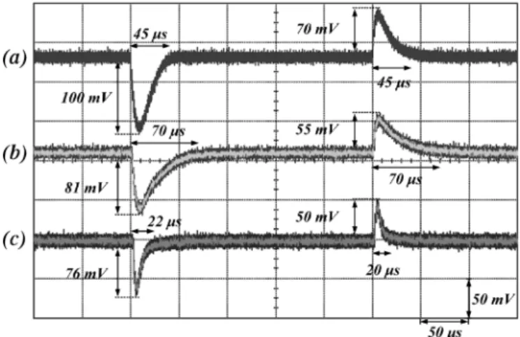
Fig. 17. Output transient waveforms of dc-dc converters with load current step-ping between 100 and 500 mA. (a) Conventional design with off-chip compen-sation. (b) With adaptive frequency control technique [17]. (c) With the fast transient provided by the single-ended capacitor multiplier.
sient response, the load current is stepped from 100 mA to 500 mA and back to 100 mA. Fig. 17 shows the transient responses for load-current rising and falling variations. The stability is promised by our proposed technique in case of load variations. Furthermore, the transient speed by our proposed technique is faster than conventional control by about 2 times, and there is only about 76% dropout voltage of the conventional design with off-chip compensation. Obviously, there is an oscillating problem existed in our proposed method compared to the tech-nique proposed by [17]. Thus, the control of fast transient is needed to be guaranteed under any worst conditions. In other words, it is important to make a tradeoff between the stability and the performance of low-dropout voltage.
V. CONCLUSION
A dc-dc converter with the bidirectional current mode ca-pacitor multiplier technique that provides on-chip compensa-tion, soft-start, and fast transient mechanisms is proposed in this paper. The bidirectional current mode capacitor multiplier tech-nique can effectively modify the position of the crossover fre-quency to a suitable position for improving the response time in case of load variations and smoothing the rising of the output voltage in case of start-up period. Experimental results demon-strate the transient speed by our proposed technique is faster than that by conventional control about two times, and there is about 76% dropout voltage of the conventional design. Both the number of components on printed circuit board and the pins of
the IC package are reduced at the sacrifice of more quiescent current about A. With the proposed bidirectional cur-rent mode capacitor multiplier technique, the performance of dc-dc converters is improved significantly and the external pins and footprint area are minimized.
ACKNOWLEDGMENT
The authors would like to thank to Chunghwa Picture Tubes, Ltd. for their help.
REFERENCES
[1] J. Zeng, A. J. Pang, C. H. Wang, and A. J. Sangster, “Flip chip assem-bled MEMS inductors,” Electron. Lett., vol. 41, no. 8, pp. 480–481, Apr. 2005.
[2] A. Makharia and G. A. Rincon-Mora, “Integrating power inductors onto the IC-SOC implementation of inductor multipliers for dc-dc con-verters,” in Proc. IECON’03. 29th Annu. Conf. IEEE, Nov. 2003, vol. 1, pp. 556–561.
[3] R. W. Erickson and D. Maksimovic´, Fundamentals of Power
Elec-tronics, 2nd ed. Norwell, MA: Kluwer, 2001.
[4] N. Mohan, T. M. Undeland, and W. P. Robbins, Power Electronics
Converters, Applications, and Design, 3rd ed. New York: Wiley, 2003.
[5] C. F. Lee and K. T. Philip, “A monolithic current-mode CMOS dc-dc converter with on-chip current-sensing technique,” IEEE J. Solid-State
Circuits, vol. 39, no. 1, pp. 3–13, Jan. 2004.
[6] H.-W. Huang, H.-H. Ho, C.-C. Chien, K.-H. Chen, G.-K. Ma, and S.-Y. Kuo, “Dithering skip modulator with a width controller for ultra-wide-load high-efficiency dc-dc converters,” in Proc. IEEE Custom
In-tegrated Circuits Conf. .(CICC), Sep. 10–13, 2006, pp. 643–646.
[7] G. A. Rincon-Mora, “Active capacitor multiplier in Miller-compen-sated circuits,” IEEE J. Solid-State Circuits, vol. 35, no. 1, pp. 26–32, Jan. 2000.
[8] J. Silva-Martinez and A. Vazquez-Gonzalez, “Impedance scalers for IC active filters,” in Proc. IEEE Int. Symp. Circuits Syst. ISCAS’98. , May 31–June 3 1998, vol. 1, pp. 151–154, vol. 1.
[9] S. Solis-Bustos and J. Silva-Martinez, “A 4 Hz low-pass continuous-time filter,” in Proc. IEEE Int. Conf. Electron., Circuits, Syst., Sep. 7–10, 1998, vol. 1, pp. 169–172, vol. 1.
[10] S. Solis-Bustos, J. Silva-Martinez, F. Maloberti, and E. Sanchez-Sinencio, “A 60-dB dynamic-range CMOS sixth-order 2.4-Hz low-pass filter for medical applications,” IEEE Trans. Circuits Syst. II:
Analog Digital Signal Process., vol. 47, no. 12, pp. 1391–1398, Dec.
2000.
[11] Y. Tang, M. Ismail, and S. Bibyk, “Adaptive Miller capacitor mul-tipliers for compact on-chip PLL filter,” Electron. Lett., vol. 39, pp. 43–45, Jan. 2003.
[12] H.-W. Huang, H.-H. Ho, C.-J. Chang, K.-H. Chen, and S.-Y. Kuo, “On-chip compensated error amplifier for fast transient dc-dc con-verters,” in Proc. IEEE Int. Electro/Inf. Technol. Conf., May 2006, pp. 103–108.
[13] H.-W. Huang, H.-H. Ho, C.-C. Chien, K.-H. Chen, G.-K. Ma, and S.-Y. Kuo, “Fast transient dc-dc converter with on-chip compensated error amplifier,” in Proc. 32nd Eur. Solid-State Circuits Conf., Sep. 2006, pp. 324–327.
[14] B. Razavi, Design of Analog CMOS Integrated Circuits. New York: McGraw-Hill, 2001.
[15] G. Palumbo and S. Pennisi, “A high-performance CMOS voltage fol-lower,” in Proc. IEEE Int. Conf. Electron., Circuits Syst., Sep. 1998, vol. 2, pp. 21–24.
[16] C.-J. Chang and K.-H. Chen, “Bidirectional current-mode capacitor multiplier in dc-dc converter compensation,” in Proc. IWSOC, Jul. 2005, pp. 111–116.
[17] H.-W. Huang, C.-Y. Hsieh, K.-H. Chen, and S.-Y. Kuo, “Adaptive fre-quency control technique for enhancing transient performance of dc-dc converters,” in Proc. IEEE 33nd Eur. Solid-State Circuits Conf., Sep. 11–13, 2007, pp. 174–177.
Ke-Horng Chen received the B.S., M.S., and Ph.D. degrees in electrical engineering from National Taiwan University, Taipei, Taiwan, R.O.C., in 1994, 1996, and 2003, respectively.
He is an Assistant Professor of the Department of Electrical and Control Engineering National Chiao Tung University (NCTU), Hsinchu, Taiwan, R.O.C. He organized a mixed-signal and power manage-ment IC Laboratory, NCTU. He was a part-time IC designer in Philips, Taipei, from 1996 to 1998. He was an Application Engineer with Avanti, Ltd., Taiwan, from 1998 to 2000. From 2000 to 2003, he was a Project Manager with ACARD, Ltd., where he worked on the designs of the power management IC. His current research interests include power management ICs, mixed-signal circuit designs, display algorithm and driver designs of LCD TV, RGB color sequential backlight designs for OCB panels, and low-voltage circuit designs. He has published more than 25 papers in journals and conferences, and also holds several patents.
Chia-Jung Chang was born in Taipei, Taiwan, R.O.C., in 1981. He received the B.S. degree in electrical engineering from National Taiwan Univer-sity of Science and Technology, Taipei, Taiwan, in 2003 and the M.S. degree in electrical and control engineering from National Chiao Tung University, Taiwan, in 2005.
He is currently with EMP, Inc., Taiwan, and en-gaged in power management IC development.
Te-Hsien Liu was born in Taipei, Taiwan, R.O.C., in 1982. He received the B.S. degree in electrical en-gineering from National Taipei University of Tech-nology, Taipei, in 2004, and the M.S. degree in elec-trical and control engineering from National Chiao Tung University, Hsinchu, Taiwan, in 2007.
He joined Novatek Corporation, Hsinchu, Taiwan, in 2007, and his research interests include power management system designs and analog integrated circuits for portable devices.