國 立 交 通 大 學
環 境 工 程 研 究 所
碩 士 論 文
晶體內部與表面摻雜釩離子對二氧化鈦光觸媒
物化特性與光催化活性之影響
Effect of surface and lattice vanadium ions on the
physicochemical and photocatalytic properties
of TiO
2
研究生:劉維斯
誌謝
經過三年酸甜苦辣的碩士生涯,我成長了,在這三年的歷練中,我學會
了獨立思考以及對事情的處理態度,這都要感謝我的指導教授 張淑閔老
師,老師除了教導我學業方面的知識外,還教會我很多做人做事的道理,
這些對我的人生都有很大的助益。也謝謝陳登銘老師、董瑞安老師、徐雍
鎣老師對本論文悉心指正並提供許多建議,使本論文更趨於充實完善。
此外,要感謝傑耀學長與品欣學姐對於我研究方面的引導以及精神方面
的鼓勵,因為有你們的支援,我才能走完全程;還有同窗友人品涵跟棈榮,
因為有你們的陪伴,使我的碩士生活一點都不孤單;學妹小 G、姿吟、真端
以及學弟胥哥,你們的加入讓實驗室變成一個大家庭,在這裡真的很感謝
實驗室的大家,因為你們的包容以及支持,讓我能順利完成畢業論文;我
要特別謝謝中興貴儀中心 EPR 操作員 吳宜瑾小姐,提供給我很多研究資料
以及建議;最後,我要感謝我的家人,因為你們的經濟支援以及精神加油,
讓我沒有後顧之憂,我愛你們。
僅以本文獻給所有關心我與曾經幫助過我的人。
維斯 謹誌
中華民國 98 年 8 月
中文摘要
本研究利用溶膠-凝膠法(sol-gel)及表面溶膠-凝膠法(surface sol-gel)製備釩離子摻雜
之二氧化鈦(TiO2),並探討晶體內部(bulk doping)或表面(surface doping)釩離子對於 TiO2
材料及物化特性之影響。研究結果顯示單純 TiO2經 300C 鍛燒後呈現 69.9 wt%的銳鈦 礦(anatase)與 31.1 wt%的金紅石,同時銳鈦礦的平均晶粒為 6.1 nm,巨體摻雜後並未明 顯改變 TiO2晶粒尺寸,其晶粒大小範圍為 6.0 至 6.5 nm 間,然而在 V/Ti 比例高於 1.27 10-3 時完全抑制金紅石晶相 (Rutile)的形成,此外,由於鍛燒溫度略高於坦曼溫度,所 以釩會遷移至表面形成 V2O5晶相。由低濃度摻雜釩的 UV-Vis 圖譜中,發現巨體摻雜 TiO2於 250~320 nm 間有 V5+吸收波峰產生,證實摻雜釩於晶體內部會於 TiO2能帶間導 入額外能階,然而當 V/Ti 莫爾比高於 1.00 %,部分 V5+會還原成 V4+,而因為 V4+會同 時捕捉電子電洞降低表面電荷轉移,所以降解 0.01 mM Rhodamine (RhB)之擬一階反應 速率常數隨著晶格內釩離子濃度的增加,而從 5.20×10⁻²降至 1.50×10⁻² 1/min,利用 EPR 偵測觸媒表面 OH 自由基,其積分面積從 5.40×10⁷降至 5.50×10⁶,證實電子轉移的效率 會隨晶格內釩離子濃度增加而變差。相較下,表面摻雜對 TiO2 的微結構及電子結構並 無巨觀的影響,但表面摻雜釩的反應速率常數卻隨著表面 V5+濃度增加而從 5.20×10⁻²提
升至 9.80×10⁻²¹/min,當 V/Ti 約為 1.0010-2時,表面摻雜 TiO
2的反應速率數高於內部 摻雜觸媒的六倍,此原因為表面的 V5+易使電子累積於 TiO 2表面,增進表面電荷轉移速 率(觸媒表面 OH 自由基積分面積從 2.07107 提升至 4.22107 ),因此表面摻雜比巨體摻 雜更可提高 TiO2光催化活性。
Abstract
The aim of this study was to investigate the effects of bulk and surface lattice dopings on physicochemical properties and photocatalytic activities of V-doped TiO2. The sol-gel-derived TiO2 exhibited 69.9 and 31.1 wt % of anatase and rutile phase, respectively. In addition, the crystallite size of the anatase TiO2 was 6.1 nm. Lattice vanadium ions had no effect on crystal size of TiO2, ranging between 6.0-6.5 nm. However, lattice vanadium ions completely inhibited the formation of rutile as the V/Ti ratio is as high as 1.2710-3
. V2O5 crystals were observed on the surface of TiO2 since vanadium ion diffused to surface when the calcination temperature was higher than its Tammann temperature. The UV-vis spectra show that bulk doping resulted in an additional absorption band centered at 289 nm. This phenomenon indicated that incorporation of V5+ions into the bulk lattice of TiO2at low vanadium concentrations (V/Ti ratio < 1.0010-2
) introduced extra energy levels in the conduction band. When V/Ti atomic ratio was higher than 1.00 %, some V5+were partially reduced to V4+ which acted as charge recombination centers. Pure TiO2 exhibited a rate constant of 5.20×10⁻² min-1 for the photocatalytic degradation of Rhodamine B (RhB). Bulk doping decreased the photocatalytic activity to from 5.20×10⁻²to 1.50×10⁻²min-1when the V/Ti ratio increased from 4.41×10⁻⁵ to 1.22×10⁻². In addition, the integrated area of generated •OHon the surface of photocatalysts, which were calculated by EPR, decreased from 5.40×10⁷ to 5.50×10⁶. The results indicated electrons diffuse to surface hardly. In contrast, surface doping had little effects on the micro- and electronic structures of TiO2. Nevertheless, the photoactivity was enhanced from 5.20×10⁻² to 9.80×10⁻² min-1 upon increasing vanadium concentration. The photoactivity of the surface doped TiO2 was six times higher than that of bulk doped ones at the V/Ti ratio of 1.0010-2
. Such enhancement is due to that surface-V5+ promotes diffusion of electrons to surface that further facility charges transfer to reactants. According to integrated area of surface doped materials, which increased from 2.07107 to 4.22107
, it indicate the electrons diffuse to surface efficaciously. Therefore, surface doping greatly improve the degradation efficiency, while bulk ones lad to detrimental effects on the photocatalytic activity.
Content Index
誌謝 ... I
中文摘要 ...II
ABSTRACT... III
CONTENT INDEX... IV
FIGURE CAPTIONS ...VII
TABLE CAPTIONS ... XI
CHAPTER 1
INTRODUCTION ... 1
1-1 M
OTIVATION... 1
1-2 O
BJECTIVES... 2
CHAPTER 2
BACKGROUND AND THEORY ... 3
2-1 T
IO
2SEMICONDUCTOR PHOTOCATALYSTS... 3
2-1-1 Background and material properties...3
2-1-2 Principle of photocatalysis...9
2-1-3 Photoassisted degradation of Rhodamine B ...13
2-2 S
YNTHESIS TOWARD METAL OXIDE... 14
2-2-1 Sol-gel method...14
2-2-2 Surface sol-gel method...18
2-3 D
OPINGT
IO
2WITH IMPURITIES... 20
2-4 B
ULK AND SURFACE DOPING SITES... 26
CHAPTER 3
MATERIALS AND METHODS ... 29
... 33
3-4 C
HARACTERIZATION... 36
3-4-1 X-ray photoelectron spectroscopy (XPS)...36
3-4-2 Time-of-Flight Secondary Ion Mass Spectrometer (TOF-SIMS)...37
3-4-3 Scanning electronic microscopy (SEM)...37
3-4-4 X-ray diffractometry...38
3-4-5 UV/Vis diffuse reflectance spectroscopy (UV-Vis DRS) ...39
3-4-6 Inductively Coupled Plasma Mass Spectromstry (ICP-MS) ...39
3-4-7 Specific surface area ...39
3-4-8 Electron paramagnetic resonance (EPR) ...39
3-4-9 Transmission Electron Microscope (TEM)...41
3-5 P
HOTOCATALYTIC OFR
HB
DECOMPOSITION... 41
CHAPTER 4
RESULTS AND DISCUSSION ... 43
4-1 C
HEMICAL COMPOSITIONS... 43
4-2 M
ORPHOLOGY... 45
4-3 M
ICROSTRUCTURES... 47
4-4 UV-V
ISIBLE ABSORPTION... 53
4-5 P
HOTOCATALYTIC ACTIVITY... 60
4-6 EPR
STUDIES OF BULK AND SURFACE DOPING MATERIALS... 67
CHAPTER 5
CONCLUSIONS ... 82
REFERENCES ... 83
APPENDIX A
EXPERIMENTAL PARAMETERS... 91
APPENDIX B
INSTRUMENT PRINCIPLE ... 93
Appendix B-1 Time-of-Flight Secondary Ion Mass Spectrometer ...93
Appendix B-2 X-ray powder diffractometry (XRPD) ...94
Appendix B-3 UV-vis diffuse reflectance spectroscopy (DRS)...96
Appendix B-4 Electron paramagnetic resonance (EPR) ...97
APPENDIX D.
ESCA ANALYSIS ... 103
APPENDIX E
BULK DOPED MATERIALS WITH HIGH
VANADIUM IONS ... 106
APPENDIX F
VANADIUM-DOPED ON THE SURFACE OF
TIO
2... 108
APPENDIX G
REDOX POTENTIAL ...111
APPENDIX H
LANGMUIR-HINSHELWOOD KINETICS . 112
Figure Captions
Figure 2-1 The density of electronic states of TiO2...4
Figure 2-2 Variation of enthalpies of anatase, brookite, and rutile as a function of particle size. ...6
Figure 2-3 The crystal phases of TiO2. ...7
Figure 2-4 UV-Vis reflectance spectra of size-quantized TiO2...8
Figure 2-5 The formation of a space charge layer in a large and small semiconductor particle in equilibrium with a solution redox system. ...8
Figure 2-6 Schematic photoexcitation in a solid followed by deexcitation events. ...9
Figure 2-7 Opticalabsorption for(a)hν= Eg,(b)hν > Eg,and (c)hν < Eg. ...10
Figure 2-8 The energies for various semiconductors in aqueous electrolytes at pH = 1... 11
Figure 2-9 Kinetics of the primary steps in photoelectrochemical mechanism. Where TiOH represents the primary hydrated surface functionality of TiO2, ecb- is a conduction-band, etr- is a trapped conduction band electron, hvb+ is a valence band hole, Red is an electron donor (i.e., reductant), Ox is an electron acceptor (i.e., oxidant), [Ti4+OH ˙ ]+is the surface-trapped valence band (VB) hole (i.e., surface-bound hydroxyl radical), and [Ti3+OH] is the surface-trapped conduction band (CB) electron. And the arrow lengths are representative of the respective time scales... 11
Figure 2-10 Secondary reactions with activated oxygen species in the photoelectrochemical mechanism. ...12
Figure 2-11 Electron-transfer processes (a) for UV irradiation of TiO2 with the self-photosensitized pathway (b) under visible light irradiation which subsequent to excitation of RhB dye...13
Figure 2-12 Formation and competitive reactions of •OH radicals during visible light irradiation of Rhodamine B. ...14
Figure 2-13 The process of sol-gel under acid condition. (a)Hydrolysis, (b)Condensation, and (c)Gelation. ...16
Figure 2-14 Gel process sequence. ...16
Figure 2-15 The relationship between gelation times and H2O:alkoxide ratio. ...17
Figure 2-16 The different structure of particles depend on pH. ...18
Figure 2-17 Schematic representation of the surface sol-gel process. ...19
Figure 2-18 Detail of liquid flow patterns of the containous process. U is the withdrawal speed, S is the station point, δis the boundary layer, and h is the thickness of the fluid film..20
Figure 2-19 The production prepared by sol-gel-derived with different processes. ...20
Figure 2-20 The structure of surface doped materials...21
Figure 2-21 Proposed V site transformations for V/TiO2in surface doped materials (A) and for bulk doped materials (B). [H] for models a and c indicates the presence/absenceof hydrogen cannot be determined...22
Figure 2-22 The bonding diagram of the TiO2 perfect crystal (rutile) proposed by Soratin and Schwarz...23
Figure 2-23 The DOS of metal-doped TiO2(Ti1-xAxO2: A=V or Ti). Gray lines means total DOS and black linesshowsdopant’sDOS.5 ...24
Figure 2-24 Band model of Ti1-xVxO2 film electrodes at bias potential of 1 V vs. SCE in an electrolyte solution. ...24
Figure 2-25 The photochemical mechanism in the present of transition metal ions...25
Figure 2-26 The energy level diagram calculated using large cluster models of (Ti15O56) 52-and (Ti11O34)24-O* corresponding to the bulk and surface of rutile TiO2. ...27
Figure 2-27 Surface and bulk electron carrier trapping...28
Figure 3-1 Flow chart of experimental design in this study. ... 30
Figure 3-2 The chemical structure of RhB. ...30
Figure 3-3 The synthetic process of bulk doped materials. (a) the flow charts of the synthesis and (b) the recipes of precursor solutions. ...32
Figure 3-4 The synthetic process of surface doped materials. (a) the flow charts of the synthesis of surface doped materials, (b) the recipes of precursor solutions, and (c) the surface sol-gel processes for coating. ...34
Figure 3-5 A design chart and a photograph of surface sol-gel system...35
Figure 3-6 The geometric structure of pure, bulk and surface doped TiO2. ...36
Figure 3-7 The UV lamp spectral distribution...40
Figure 3- 8 The UV-Vis spectrum of 0.01 mM RhB. ...41
Figure 3-9 A design chart for photocatalysis reactor and A photograph of photocatalytic reactor. ...42
Figure 4-1 The morphology of pure TiO2calcined at (a) 150 °C for 3 h and (b) 150 and 300 °C for 3 h. ... 45
...48 Figure 4-5 The effect of bulk defect on growth of crystal...49 Figure 4-6 The GI-XRD patterns of bulk doping materials. ...50 Figure 4-7 The XRD patterns of surface doped materials at different vanadium ions concentration. ...51 Figure 4-8 The GI-XRD patterns of surface doped materials. ...52 Figure 4-9 The microstructures of bulk and surface doped TiO2. ...53 Figure 4-10 UV-Vis DRS spectra of TiO2. The red solid line: Upper conduction band. The blue dash line: Lower conduction band...54 Figure 4-11 The UV-visible absorption spectra of all bulk doped materials at different vanadium ions concentration, except VT 1.22×10⁻²which is shown in inside graph. ...55 Figure 4-12 Energy levels of impurity ions in rutile. ...56 Figure 4-13 The concept of electronic structure for bulk doping materials. (a) low vanadium ions (< 1 mole%); (b) high vanadium ions (i.e. VT 1.22×10⁻²). ...57 Figure 4-14 The UV-visible absorption spectra of the surface doped materials at different vanadium ions concentrations. ...58 Figure 4-15 Schematic band energy diagram for the TiO2/V2O5composite semiconductor. 59 Figure 4-16 The electronic structure of surface doping materials...59 Figure 4-17 The decoloration of 0.01 mM RhB by pure and bulk doped TiO2under (a) 305 nm and (b) 365 nm UV irradiation. ...61 Figure 4-18 The rate constants of bulk doped materials at various vanadium ions concentration compared with pure TiO2under (a) 305 nm UV and (b) 365 nm UV irradiation. ...62 Figure 4-19 The concept of higher content V4+at substitutional site in Q-size TiO2lattice. 64 Figure 4-20 The decoloration of 0.01 mM RhB by surface doping materials at various vanadium ions concentration compared with pure TiO2 under (a) 305 nm UV and (b) 365 nm UV irradiation...65 Figure 4-21 The rate constants of surface doped materials at various vanadium ions concentration compared with pure TiO2under (a) 305 nm UV and (b) 365 nm UV irradiation. ...66 Figure 4-22 The difference in EPR spectra of pure TiO2before and after irradiation of UV at 77K. ...68 Figure 4-23 EPR spectra of pure and bulk doped TiO2at different vanadium contents at 77K in the dark. (a) The bulk V/Ti ratios ranged 0-5.09×10⁻⁴ and (b) The bulk V/Ti ratios in the
range 1.27×10⁻³-1.22×10⁻². ...70 Figure 4-24 The EPR spectra of vanadium ions doped in TiO2...71 Figure 4-25 EPR spectra of bulk doped materials at various vanadium concentrations under UV irradiation at 77K. ...71 Figure 4-26 The concept of bulk doping materials at low vanadium concentration. ...72 Figure 4-27 The concept of bulk doping materials at intermediate vanadium concentration. ...73 Figure 4-28 The concept of bulk doping materials at high vanadium concentration. ...74 Figure 4-29 EPR spectra of surface doping materials at various vanadium concentration in the dark at 77K ...74 Figure 4-30 EPR spectra of surface doped materials at various vanadium concentrations under UV light at 77K. ...76 Figure 4-31 The concept of surface doped materials ...77 Figure 4-32 TheERP spectrum of•OH-DMPO in the dark and UV irradiation...80 Figure 4-33 The mechanisum of•OH-DMPO adducts formed upon trapping of OH radicals by the DMPO molecules. ...81
Table Captions
Table 2-1 Milestone of TiO2-related reference ... 5
Table 2-2 The relationship between crystal size and stable phase . ... 6
Table 4-1 The bulk and surface V-to-Ti atomic ratios of bulk doped TiO2. ... 43
Table 4-2 The bulk and surface V-to-Ti atomic ratios of surface doped TiO2...44
Table 4-3 The crystallite sizes, d-spacing of materials and weight ratio of rutile phase of bulk doped TiO2...48
Table 4-4 The crystallite sizes of materials and weight ratio of rutile phase of surface doped TiO2...51
Table 4-5 The band gap energy of bulk doped TiO2...56
Table 4-6 The band gap energy of surface doped TiO2...58
Table 4-7 The rate constants of bulk doped TiO2 at various vanadium concentration compared with pure TiO2under 365 and 305 nm UV irradiation. ...63
Table 4-8 The rate constants of the surface doped TiO2at various V/Ti ratios. ...67
Table 4-9 g value for various paramagnetic species...78
Table 4-10 Theintegrated areasof•OH-DMPO signals obtained from the bulk doped TiO2 suspension under UV irradiation. The suspensions were aerated with O2 for 30 min in the dark before irradiation. ...80
Table 4-11 Theintegrated areasof•OH-DMPO signals obtained from the surface doped TiO2suspension under UV irradiation. The suspensions were aerated with O2 for 30 min in the dark before irradiation. ...81
Chapter 1
Introduction
1-1 Motivation
Titanium dioxide (TiO2) is the mostly used photocatalysts for decomposition of environmental pollutants because of cheap, nontoxic, and highly chemical stable characteristics1. To improve its photocatalytic activity, impurities including transition metal ions (Fe, V)2-6 and non-metal ions (N, C)7-9 were doped into the TiO2 lattice to modify its microstructures and electronic structures. The kinds of contributions of the modification to the photocatalytic activity include (1) inhibition of recombination by increasing the charge separation; (2) increase in the wavelength response range (i.e. excitation of wide band gap semiconductors by visible light); and (3) change in the selectivity or yield of a particular product.10-12
The types and chemical states of dopants determine the microstructure, band gaps and photoactivity of metal-doped TiO2because of different electronic configurations and sizes of the ions. Panagiotis Bouras et al.4 reported Fe3+, Cr3+and Co2+ denoting visible-light photocatalyst were used to decompose Basic Blue 41, while photodegradation efficiency of the doped material was achieved only at very high doping levels. Kemp et al.13reported that doping of rutile with Cr3+, V5+or Mn2+ reduces its photoactivity, while doping with Mo5+ or W5+ enhances its photocatalytic performance. Martin et al.14 doped TiO2 with V5+ via coprecipitation method which also resulted in reduced photoreactivity. However, Klosek and Raftrey15 reported V-doped TiO2 extended the wavelength range of the catalyst into the visible region (396-450 nm) and greatly improved the photocatalytic activity of titania under solar light irradiation. However, the effects of vanadium ions on the photocatalytic activity of TiO2are still controversial.
Such uncertainties are attributed to the multiple oxidation states of vanadium ions (V3+, V4+and V5+) which result in different nonstoichiometry and bandgaps of TiO2. In addition, the doping sites affect the bulk and surface crystalline structure, thereby controlling the utility of photo-generated charge carriers. Balikdjian et al.16reported that the presence of V species in the bulk lattice of anatase inhibited the transformation of anatase into rutile. Generally, anatase TiO2exhibits higher photocatalytic activity than rutile. In addition, the particle sizes of TiO2become small after doping with V5+ions.10 Large amounts of surface defects of the
activity.
In contrast to deep trapping in the bulk, defects on the surface sites not only trap charge carriers but also deliver the trapped charges to adsorbed reactants. The trapping time of carrier electrons at the surface level become longer with an increase in △Esurface(△Esurfacemeans the energy different LUMO of bulk TiO2 and the lowest level of transition metal).19 Moreover, surface defects can cause unsaturated coordination of Ti4+and oxygen vacancies which serve as active sites for photocatalysis.20 Chang et al.21 reported Lewis acid sites of surface modified TiO2readily chemisorbed water to generate reactive hydroxyl radicals. In addition, electron transfer from conduction band to adsorbed O2 was improved for efficient mediated photocatalysis. However, the effects of doping sites of vanadium ions on the physicochemical and photocatalytic properties have not been documented yet.
1-2 Objectives
This study aims to investigate the influence of bulk and surface doping sites on the micro-, electronic- structures and chemical states of V-doped TiO2. The bulk and surface doped materials were prepared by sol-gel and surface sol-gel, respectively. In addition, the charge trapping and interfacial charge transfer properties were analyzed using EPR. The photocatalytic activities of the doped TiO2 were determined in terms of decoloration of rhodamine B. The photocatalytic behavior of the doped TiO2 with respect to its bulk and surface defects were discussed based on the physicochemical properties.
Chapter 2
Background and theory
2-1 TiO
2semiconductor photocatalysts
2-1-1 Background and material properties
In 1972, Fujishima and Honda successfully found TiO2 nanoparticles that can be used in photocatalytic reactors for degrading pollutions in water or air.22 Afterward, scientific studies on development and fabricate of photocatalysis by semiconductor was blossomed, which are listed in Table 2-1. In order to improve the efficiency of photoactivity, some surface modification methods have been proposed for the development of advanced photocatalysts, including composite semiconductors, surface sensitization, and transition metal doping.5, 9, 17 Nowadays, TiO2 has been widely used in industrial application such as photocatalysis23, solar energy cell24, and gas sensors.25
TiO2possesses a bandgap of 3.0-3.2 eV. Figure 2-1 shows the total density of electronic states of TiO2. The conduction band (CB) and valence band (VB) of TiO2mainly consist of the Ti 3d and O 2p states, respectively. Generally, TiO2can be excited by energy in terms of heat or photon. The excited semiconductor has electrons and holes pairs within conduction and valence bands for further redox reactions, respectively. Thus, the principle of photocatalysis is the transformation of excited electrons and holes which play important roles in this system.17, 26
Table 2-1 Milestone of TiO2-related studies.
Year Authors The results and findings Ref.
1972 Fujishima et al.
First finding about electrochemical photolysis of water at a semiconductor electrode.
22
1987 Matthews et al.
Photooxidation of organic impurities in water using thin films of titanium dioxide.
28
1994 Choi et al. The summarization of metal-ion dopants in quantum-sized TiO2.
29
1994 Martin et al. Photochemical mechanism of quantum-sized vanadium-doped TiO2particles
14
1995 Linsebigler et al.
Mechanisms of photocatalysis of TiO2, including surface modification method.
17
1999 Litter et al. The mechanism of photocatalytic systems on transition metal ions doped in TiO2.
30
2002 Haber et al. Surface doping of rutile by vanadium. 18
2003 Diebold et al. The surface science of titanium dioxide. 31
2003 Weckhuysen
et al.
Chemistry, spectroscopy and the role of supported vanadium oxides in heterogeneous catalysis
32
2004 Lee et al. Electronic surface state of TiO2electrode doped with transition metals, studied with cluster model and DV-X alpha method
19
2007 Xin et al. The mechanisms of photoinduced carriers separation and recombination for Fe3+–TiO2photocatalysts
3
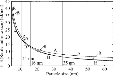
TiO2 has three types of crystalline structures: anatase, rutile, and brookite. At higher temperature above 623 K, anatase starts to transform to brookite and /or rutile, and then brookite transforms to rutile. At lower temperature below 623 K, the transformation between anatase and brookite may be reversible. The activation energy of transformation from anatase to brookite (11.9 KJ mol-1) is much lower than that from brookite to rutile (163 KJ mol-1). This means the brookite → rutile transformation occurs under higher temperature,
transforms to brookite and then transforms to rutile.
Figure 2-2 Variation of enthalpies of anatase, brookite, and rutile as a function of particle size.33
Table 2-2 The relationship between crystal size and stable phase33. Crystal size Most stability phase
< 11 nm Anatase
11 ~ 35 nm Brookite
> 35 nm Rutile
Figure 2-3 shows the crystalline structures of anatase and rutile TiO2. Each Ti4+ion is surrounded by an octahedron of six O2- ions. In the rutile structure, each octahedron is in contact with 10 neighboring octahedrons (two sharing edge oxygen pairs and eight sharing corner oxygen atoms), while in the anatase structure each octahedron is in contact with eight neighbors (four sharing an edge and four sharing a corner). These differences in lattice structures cause different mass densities and electronic band structures between anatase and rutile.17 The octahedron in anatase is significantly distorted so that its symmetry is lower than orthorhombic. Therefore, anatase shows a higher adsorptive ability toward organic compounds23 and lower rate of charge recombination34, while rutile shows a lower bandgap energy and higher thermal stability.17
Figure 2-3 The crystal phases of TiO2.17
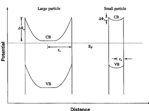
When the crystallite dimension of a semiconductor particle falls below a critical radius of approximately 10 nm, the band gap increases and the band edges shift to yield larger redox potentials, as shown in Figure 2-4. Thus, the size-quantized semiconductor TiO2 particles may result in increased photo-efficiencies for systems in which the rate-limiting step is charge transfer. Figure 2-5 shows a high photo-reactivity of quantum-size TiO2 due to the lack of band bending, while both electrons and holes are readily available at the interface (or vary close). However, size-quantized TiO2 have been found to be less photoactive than their bulk-phase cases because surface speciation and surface defect density reduce photoactivity. Thus, the positive effects of increased over potentials (i.e., difference between Evband Eredox) on quantum yields could be offset by unfavorable surface speciation and surface defects due to the preparation method of size-quantized semiconductor particles.26
Figure 2-4 UV-Vis reflectance spectra of size-quantized TiO2.26
Figure 2-5 The formation of a space charge layer in a large and small semiconductor particle in equilibrium with a solution redox system.10
2-1-2 Principle of photocatalysis
Heterogeneous photocatalysis is one of the popular techniques for decontamination of air and wastewater, because photocatalyst can transform solar energy into chemical energy to degrade pollutants. The basic principles of heterogeneous photocatalysis can be simply summarized as follows. After the generation of charge carriers by absorbing UV-light with the energy over the band gap, the charge carriers undergo trapping, recombination, detrapping, and migration to the surface, as seen in Figure 2-6.14, 26, 29
Figure 2-6 Schematic photoexcitation in a solid followed by deexcitation events.17
Figure 2-7 shows the basic transitions in a semiconductor, including intrinsic and extrinsic transitions. When the semiconductor is irradiated with UV light, photons are absorbed to create electron-hole pairs while the photon energy (hν)is equal to or larger than the bandgap energy (Eg). Ifhν isgreaterthan Eg, excess energy is dissipated as heat, as shown in Figure 2-7 (b). These processes are called intrinsic transitions or band-to-band transitions. In addition,forhν islessthan Eg, a photon will be absorbed by energy states which are created by chemical impurities or physical defects. Above performance is defined extrinsic transition, as shown in Figure 2-7 (c).35
Figure 2-7 Opticalabsorption for(a)hν= Eg, (b)hν > Eg, and (c)hν < Eg.35
For thermodynamic view point, the band energy positions and the redox potential of semiconductors determine the ability of charge transfer to acceptors. Adsorbed pollutants can be reduced by conduction band (CB) electrons if they have redox potential more positive than the Vfb of the CB. Besides, the pollutants can also be oxidized by valence band (VB) holes if they have reduction potential more negative than the Vfb of the VB.30, 36 Figure 2-8 shows the band edge positions for various semiconductors. Left axis presents the internal energy scale relative to the vacuum level and right one shows the comparison with normal hydrogen electrode (NHE). The positions are originated from the flat band potentials in a contact solution of aqueous electrolyte at pH = 1. Therefore, more pollutants can be decomposed in case the band gap is larger.
Figure 2-8 The energies for various semiconductors in aqueous electrolytes at pH = 1.17
Figure 2-9 shows the time scale of charge carrier generation, trapping, recombination, and interfacial transfer. After charge-carrier generation (~fs), recombination is mediated primarily by Ti3+in the first 10 ns. Valence-band holes are sequestered as long-lived TiOH+ after 10 ns. TiOH is reformed by recombination with conduction band electrons or oxidation of the substrate on the time scale of 100 ns. However, the electrons transfer from CB to surface is micro-seconds, so the phenomena is determine step in photocatalysis.26
[Ti4+OH˙]+ is the surface-trapped valence band (VB) hole (i.e., surface-bound hydroxyl radical), and [Ti3+OH] is the surface-trapped conduction band (CB) electron. And the arrow lengths are representative of the respective time scales.26
Hoffmann et al.26 and Hurum et al.37 reported that the photogenerated holes recombine with surface electrons easily. So, the present of oxygen not only act as an electron acceptor, but also perform H2O2which is a direct source of hydroxyl radicals.26 Besides, the hydroxyl radical (˙OH) was proposed to be the primary oxidant in the degradation of organic water contaminants.38, 39 Therefore, the processes of secondary reactions with activated oxygen are summarized in Figure 2-10. Figure 2-10 shows the oxidation occur by either oxidation via the surface-bound hydroxyl radical (i.e., trapped hole at the TiO2 surface) or via the other radicals (i.e., formation of superoxide radicals). And the reduction occurred by directly electrons diffusion under lower conduction states of TiO2. Hence, it is important for the present of oxygen which plays as the primary electron acceptor.39
Figure 2-10 Secondary reactions with activated oxygen species in the photoelectrochemical mechanism.26
2-1-3 Photoassisted degradation of Rhodamine B
In general, the TiO2degrade many organic pollutants and to mineralize completely under UV irradiation.26, 40 In order to expand the wavelength range in visible light for the photocatalysts, surface sensitization of TiO2via chemical or physic adsorbed dyes molecular were used to promote the efficiency of the charge carrier separation with visible irradiation.12, 17, 40
For example, the chemisorbed RhB is excited at wavelengths longer than 470 nm to produce singlet and triplet states (denoted here simply as RhB*ads). Subsequently, RhB*ads injects an electron into the conduction band (or to some surface state) of TiO2with RhB being converted to the radical cation RhB•+, as shown in Figure 2-11. Afterward, the electrons in the conduction band of TiO2 react with adsorbed oxidants, usually O2, to produce reactive oxygen radicals (Equation 2-3 to 2-6).12 Figure 2-12 shows the de-ethylation reaction since the radical cation RhB•+ultimately reacts with reactive oxygen radicals and/or molecular oxygen.40 Moreover, oxygen plays an additional important role to inhibit recombination between RhB•+and e-CB. In addition, the secondary radical processes occurred might lead to mineralization. The semiconductor TiO2 acts as an electron-transfer mediator and the oxygen as an electron acceptor leading to efficient separation of the injected electron and the radical cation, thereby facilitating the degradation process.
Figure 2-11 Electron-transfer processes (a) for UV irradiation of TiO2 with the self-photosensitized pathway (b) under visible light irradiation which subsequent to excitation
ads ads h Dye Dye (2-1)
ads TiO Dyeads
Dye 2 E°= -1.09 V (2-2) 2 2 2(e ) O O TiO cb E°= -0.33 V (2-3) OOH H O2 E°= -0.037 V (2-4) 2 2 2 2 H O H O O OOH E°= +1.84 V (2-5) 2 2 2 2O O H OH OH O H E°= +0.74 V (2-6) ads
Dye (OH•, O2•-, and/or O2)→→
Degraded products (2-7)
Figure 2-12 Formation and competitive reactions of •OH radicals during visible light irradiation of Rhodamine B.22
2-2 Synthesis toward metal oxide
2-2-1 Sol-gel method
Sol-gel processes have been widely used to synthesize TiO2, because there are many advantages of the sol-gel processes include cheaper, low reaction temperature, uniform structure, extreme purity, selective of precursor and widely applications. The sol-gel process can be characterized by a series of distinct steps.41
Step 1: In order to stable solutions of the alkoxide or solvated metal precursor (the sol), so the precursor would under hydrolysis and condensation for couple days.
Step 2: After hydrolysis and condensation, gelation resulting from the formation of an oxide-or alcohol-bridged netwoxide-ork (the gel) by a polycondensation oxide-or polyesterification reaction that results in a dramatic increase in the viscosity of the solution. If so desired, the gel may be cast into a mold during this step.
until the gel transforms into a solid mass, accompanied by contraction of the gel network and expulsion of solvent from the gel pores. Ostwald ripening and phase transformations may occur concurrently with syneresis. The aging process of gels can exceed 7 days and is critical to the prevention of cracks in gels that have been cast. Step 4: Drying of the gel, to remove water and other volatile liquids from the gel network.
This process is complicated due to fundamental changes in the structure of the gel, which was occurred between 100 and 180 ºC. If isolated by thermal evaporation, the resulting monolith is termed a xerogel. If the solvent is extracted under supercritical or nearsupercritical conditions, the product is an aerogel.
Step 5: Dehydration, during which surface-bound M-OH groups are removed, thereby stabilizing the gel against rehydration. This is normally achieved by calcining the monolith at temperatures up to 800°C. Besides, the calcination processes also cause crystal structure of materials to produce.
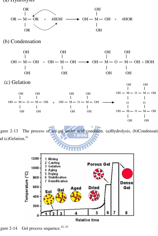
Figure 2-13 shows the reaction of sol-gel, including hydrolysis, condensation, and gelation. The hydrolysis occurs by the nuclephilic attack of the oxygen contained in water on the silicon atom as evidenced by the reaction of isotopically labeled water with TEOS that produces only unlabelled alcohol in both acid and basic catalyzed system. Besides, the polymerization to form siloxane bonds occurs by either an alcohol producing condensation reaction or a water-producing condensation reaction. Relative to different condition (i.e. pH), the typical of condensation products is monomer, dirmer, linear trimer, cyclic trimer, cyclic tetramer and higher-order rings. In basic condition, particle growth in size with decrease in number; in acid condition, the particles aggregate into three-dimensional networks and form gel. So, the structure was linear or randomly branched polymer under acid condition, while it was branched cluster under basic condition. And the final process is drying and calcination which lead to the structure of gels stable by thermal treatment.41 In addition, Figure 2-14 shows the processing steps involved in making sol-gel-derived.
M OR OR OR OR M OH OH OH OH + 4HOH + 4HOR M OH OH OH O M OH OH OH M OH OH OH OH M OH OH OH OH + + HOH
(a) Hydrolysis
(b) Condensation
M OH OH OH O M OH OH OH + M OH OH OH O M OH OH OH M OH OH O M OH OH M O OH OH O M O OH OH(c) Gelation
Figure 2-13 The process of sol-gel under acid condition. (a)Hydrolysis, (b)Condensation, and (c)Gelation.41
Figure 2-14 Gel process sequence.42, 43
Generally speaking, the transition metal systems are distinguished from silicates by greater chemical reactivity resulting from the lower electronegativity of the metal and its
ability to exhibit several coordination states, so that coordination expansion occurs spontaneously upon reaction with water or other nucleophilic regents.44 Therefore, the sol-gel processes of silicon and titanium precursors were similar, silicon was used to make example in this study. Sol-gel processes appear to be a simple operation, but several variables can influence the properties of the final products. Such as, pH of the reaction medium, water: alkoxide ratio, reaction temperature, and polarity of solvent. Therefore, by varying these processing parameters, materials with different physicochemical properties can be obtained. Thus the different parameters were introduced below.
The introduction of water to the Si(OR)2 precursor initiates hydrolysis, as shown in Figure 2-15. The water:alkoxide ratio determines the sol-gel chemistry and the structural characteristics of the hydrolyzed gel. High water:alkoxide ratios in the reaction medium ensure a more complete hydrolysis of alkoxides, favoring nucleation versus particle growth. Thus precursor solution reacts very quickly with water especially in the presence of excess of water. The rapid initial hydrolysis results a solution with a high degree of supersaturation of hydroxylated metal oxide. This leads to a high rate of nucleation and the formation of small particles or crystallites.44, 45
Figure 2-15 The relationship between gelation times and H2O:alkoxide ratio.44
the synthesis with HCl addition, so that a turbid gel was formed instead of white precipitates. HCl serves not only as an acid catalyst, but also as an electrolyte to prevent particle growth or agglomeration through electrostatic repulsion.46 Besides, under basic conditions, the silica products tend to form large agglomerates that eventually cross-link.44 Therefore, the differences between acid and base catalyzed reactions and the consequences for particle morphology are conceptually represented in Figure 2-16.
Figure 2-16 The different structure of particles depend on pH.41
The polarity of solvent affects the hydrolysis process, because the hydrolysis reaction proceeds via nuclepphilic reaction mechanism with OH- as the nucleophile. This phenomenon facilitate further attack of the nuclephile on the silion atom which is more positive charge on the silicon atom after the hydrolysis of the first alkoxy group, because OH -is a marginally better leaving group than –OR while the condensation process can occur. Thus, the rate of hydrolysis and condensation reaction followed sequence 1-butanol > methanol > 1-propanol > ethanol > 2-propanol, because the reaction rate was caused by hydrogen bonding and steric effect in solvent alcohol. If the hydrogen bonding ability is the only one factor, then increasing hydrogen bonding ability of solvent decreases the mobility of water to react with TEOS while the rate of hydrolysis reaction followed order 1-butanol > methanol > 1-propanol > ethanol > 2-propanol.47, 48 However, in order to slow down the rate of hydrolysis, 2-propanol is the better chose for solvent.
2-2-2 Surface sol-gel method
In addition to sol-gel method, surface sol-gel can fabricate ultra-thin films with molecular-scale. Figure 2-17 shows the process of surface sol-gel. This process is
composed of chemisorption of alkoxide, rinse, hydrolysis of the chemisorbed alkoxides, and drying.44, 49 The moving substrate entrains liquid in a fluid mechanical boundary layer carrying g some of the liquid toward the deposition region, where the boundary layers splits in two (see Figure 2-18). The inner layer moves upward with the substrate, while the outer layer is returned to the bath. The thickness of the deposited film is related to the position of the streamline dividing the upward- and downward-moving layers.
Therefore, there are six forces in the film deposition region govern the film thickness and position of the streamline: (1) viscous drag upward on the liquid by the moving substrate, (2) force of gravity, (3) resultant force of surface tension liquid in the concavely curved meniscus, (4) inertial force of the boundary layer liquid arriving at eh deposition region, (5) surface tension gradient and (6) the disjoining or conjoining pressure (important for films less than 1 μm thick). When the liquid viscosity and substrate speed are high enough to lower the curvature of the meniscus, then the deposited film thickness balances the viscous drag and gravity force.44
According to surface sol-gel principle, the process could be applied to various materials surfaces irrespective of their shape, size and structure. Besides, it is applicable to a wide range of metal precursor (metal alkoxides).49 Therefore, the reaction between the surface TiO2 hydroxyl groups with vanadia precursor molecules is therefore the best route to obtain well-defined surface concentrations of vanadium. However, Figure 2-19 shows the structure of production was prepared with different path way.
Figure 2-18 Detail of liquid flow patterns of the containous process. U is the withdrawal speed, S is the station point, δis the boundary layer, and h is the thickness of the fluid film.44
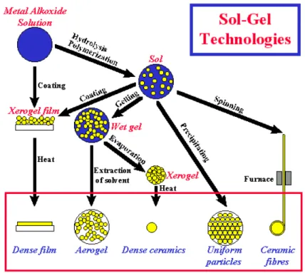
Figure 2-19 The production prepared by sol-gel-derived with different processes.42, 44
2-3 Doping TiO
2with impurities
Photocatalytic activity of a particular semiconductor system for the stated purpose is measured by several factors including the stability of the semiconductor under irradiation, the efficiency of the photocatalytic process, the selectivity of the products, and the wavelength range response. Therefore, photocatalyst for a particular use can be surmounted by modifying the surface of the semiconductor. Three benefits of modifications to
photocatalytic semiconductor systems have been studied: (1) inhibiting recombination by increasing the charge separation; (2) increasing the wavelength response range (i.e. excitation of wide band gap semiconductors by visible light); and (3) changing the selectivity or yield of a particular product. For examples, impurities like transition metal ions (Fe, V)2-5, 50, and non-metal ions (N, C)7-9 were mostly used to dope into crystalline structure of TiO2 to vary some physicochemical properties of original TiO2, including microstructure, electronic structure, and photocatalysis.
In order to define the structure of vanadium doped in TiO2, the catalysts have been studied by in situ FT-Raman. Figure 2-20 and Figure 2-21 show the structure of surface and bulk doped materials. For surface doped materials, there are two kinds of forms of VOx species attached to the TiO2surface: monomeric vanadyl and polymeric vanadates.51-53 In particular, the coordination of the surface oxygen atoms plays a key role in reactivity. All of the potentially active oxygen sites proposed to be vanadyl V=O (1030 cm-1), bridging V-O-V (822 cm-1), interface V-O-Ti, and surface Ti-O-Ti (638 cm-1). For hydrogen atomic adsorption, the most reactive sites are those located at the interface between the V2O5and the TiO2 unit (V-O-Ti), while the vanadly V=O bonds are more stable.53, 54 So, while the number of vanadium centers in the polyvanadates increase, the number of terminal V=O (930 cm-1) groups per vanadium decreases to accommodate V-O-V (822 cm-1) linkages.51-53 It meant the vanadium ions were preferred to perform V2O5 under higher vanadium concentration. For bulk doped materials, the V4+ions were substituted Ti4+of TiO2structure, because two cations have the similar ionic charge ( rV4+6c= 0.590 Å and rTi4+6c= 0.605Å).55
Figure 2-21 Proposed V site transformations for V/TiO2in surface doped materials (A) and for bulk doped materials (B). [H] for models a and c indicates the presence/absenceof hydrogen cannot be determined.55
Figure 2-22 shows the bonding diagram of the TiO2 perfect crystal (rutile). The conduction band (CB) and valence band (VB) of TiO2 mainly consist of the Ti 3d and O 2p states, respectively. Besides, the bottom of the lower CB consisting of the T dxy orbital contributes to the metal-metalinteractionsdueto theσ bonding oftheTit2g–Ti t2g states.56 Therefore, if transition metal ions doped in TiO2, the bandgap energy of TiO2shifted a lower energy due to extra energy level caused by 3d dopants (transition metal ions).5 So, in case of V/TiO2, total density of electrons is shown in Figure 2-23. The V5+/V4+redox level was lied 1.4 eV above the top of the valence band in rutile. The V4+/V3+level lies 0.8 eV below the bottom of the conduction band.29, 57 While both redox levels remain with the band gap in the TiO2colloids, both holes and electrons can be trapped by V4+which will cause disappearance of the V4+EPR signal.29, 57
In order to define hyperfine parameter of various species containing a V4+paramagnetic ion, I have used subscripts 6c, 5c and 4c to stand hexa-, penta-, and tetracorrdinated V4+ species. In this notation, vanadyl ions are formally labeled (VO2+)ic were referred to the global vanadium coordination. However, three are three distinct ligand field geometries can thus be distinguished, as shown below.58
1. Vanadly ions in a square pyramidal (VO2+)5c or in an axially distorted octahedral symmetry (VO2+)6c. (g = 1.955 ~ 1.980)
2. Vanadium ions in a tetrahedral geometry, (V4+)4c.
1.950)
Moreover, the coordination sphere of these vanadyl ions (VO2+) may then be completed either by some surface oxygen anions (O2-) of the TiO2 sublattice or by adsorbed water molecules. And (V4+)6cis shown a vanadium ions located at the center of the rutile unit cell is surrounded by a slightly distorted oxygen octahedron.58
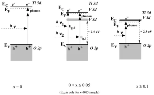
In addition, the atomic ratio of V/Ti can influence the electronic structure. Figure 2-24 showsthe band model of Ti1-xVxO2at bias potential of 1V vs. SCE in an electrolyte solution at various atomic ratio of V/Ti. For V/Ti = 0.025 and 0.05 samples, the recombination time was larger than V/Ti=0 sample, because the V 3d level in the bandgap inhibited the electron-hole recombination. But, it seemed the increasing photocurrent with the potential was stronger for V/Ti ≧0.1 samples. This can probably be ascribed to the connection of the filled V 3d level with the conduction band, which result in the semi-metal behavior. Summary, the different atomic ratio of V/Ti can influence the electronic structure of materials.
Figure 2-23 The DOS of metal-doped TiO2(Ti1-xAxO2: A=V or Ti). Gray lines means total DOS and black linesshowsdopant’sDOS.5
Figure 2-24 Band model of Ti1-xVxO2film electrodes at bias potential of 1 V vs. SCE in an electrolyte solution.59
The extra energy caused by dopant affect photocatalysis of TiO2 because the defect performed by dopants can trap either an electron or a hole alone.29 So, a general photochemical charge-trapping, recombination, detrapping, and migration mechanism in the presence of transition metal ion dopants is proposed as Figure 2-25:
Figure 2-25 The photochemical mechanism in the present of transition metal ions.29
It has hypothesized that the addition of transition metals to titania increases the rate of photocatalytic oxidation, due to the electron scavenging by the transition metal ions at the semiconductor surface through the following reaction : Mn+ + e-CB→M(n-1)+, where Mn+ represents transition metal ions.60 This reaction prevents electron-hole recombination and results in an increase rate of formation of ˙OH radical. Besides, when dopant acts as both electrons trapping and holes trapping, it would decrease the rate of recombination. For example, the present of vanadium in the TiO2lattice act as both electrons and holes trapping. Thus, the photoactivity of V5+is significantly higher than the photoactivity of V4+.29
2-4 Bulk and surface doping sites
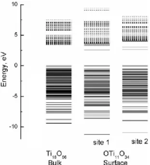
Lee et al. reported19 that the surface levels of TiO2 were the levels of mixed orbitals, which are composed of 3d orbitals of Ti and 2p orbitals of the surface oxygen. Therefore, the electronic density of bulk and surface are different, which is shown in Figure 2-26. The effect of vanadium doping positions on the electronic structure of TiO2 could be different. Most of the dopant levels related to the surface are found between conduction and valence bands of bulk TiO2. Therefore, it is expected that the doping of a transition metal to a TiO2 surface increases the surface trapping rate of carrier electrons and the trapping effect becomes larger with increasing in the atomic number of a transition metal dopant. Lee et al.19 reported that the number and energy of surface levels are deeply affected by impurities found on the surface of TiO2. And the trapping time of carrier electrons at the surface level become longer with an increase in △Esurface. (△Esurface means the energy different LUMO of bulk TiO2and the lowest dopant level). It refers that transition metal doped on TiO2surface increases the surface trapping rate of carrier electrons. However, the bulk doping site caused by transition metals performed extra energy level between VB and CB. Although the defects retard the charge recombination by trapping, the trapped electrons/holes can not migrate to substance surface for following reduction or oxidation of adsorbed reactants. Thus, the surface doping sites can promote the electrons to transfer to surface efficiently, while bulk doing sites could be detrimental to the photocatalytic activity. However, there are few papers to discuss the mechanism of photocatalysis with different V-doping positions.
Figure 2-26 The energy level diagram calculated using large cluster models of (Ti15O56) 52-and (Ti11O34)24-O* corresponding to the bulk and surface of rutile TiO2.19
Doping TiO2 with V4+/V5+ at different sites also influences the crystal structures. Balikdjian and Davidson et al16reported that the presence of V species into the bulk lattice of anatase did not affect the transformation of anatase into rutile, but the V species deposited on the surface of anatase grain boundary favored rutile transformation. In addition, the particle sizes of TiO2become small after doping with V5+ions and result in significant band bending. 10
To fully understand the influence of doping on the nature and extent of charge transfer, particle size and crystal structure need to be investigated.10, 61
In heterogeneous system, the photoactivity occurs on the surface of materials. The defects on the TiO2 surface are easily formed by thermal treatment because the oxygen vacancy site leaves an exposed Ti3+ion which may be visualized as a Ti4+ion associated with a somewhat localized electron. In addition, the exposed Ti3+atoms diffuse from the bulk to the surface during calcination, so the thermal treatment causes the incorporation of oxygen vacancy into the surface layer of TiO2. Surface trapping sites were supposed to promote the photocatalytic activity efficiency than bulk trapping sites due to a lack of surface oxygen defects. Figure 2-27 shows bulk and surface trapping sites, respectively. The electrons trapped by bulk defect called bulk trapping, and the electrons trapped by surface defect called
Chapter 3
Materials and methods
Figure 3-1 shows the flow chart of the experimental design in this study. Catalysts are synthesized with sol-gel and surface sol-gel methods.
3-1 Materials
Titanium isopropoxide (TTIP, Acros, 98 %+) and vanadium (Ⅴ) oxytriisopropoxide (VTIP, Aldrich, 99 %+) were used as the precursors of titania and vanadium, respectively. 2-propanol (C3H7OH, J.Backer, 100 %) was used as solvent to dissolve titanium isopropoxide and vanadium (Ⅴ) triisopropoxide. Rohdamine B (RhB, C28H31N2O3Cl, Sigma Aldrich, Dye content 95 %) was used as the target compound for photocatalysis and its structure is shown in Figure 3-2. Hydrogen acid (HCl, Crown, 35 ~ 37 %) was used to adjust the pH of sol solution to slow down the hydrolysis. Filter membrane (Critical, 47 mm in diameter, 0.2 μm in pore size) was used as a support for the TiO2 during its surface coating process. 5,5-dimethyl-1-pyrroline N-oxide (DMPO, Aldrich, 97%, d= 1.05 g/mL)wasused asa•OH trapped agent. The original DMPO solution was stored at –25 °C. In addition, DMPO diluted by DI water were decay, so the solution need to use immediately for least 2 two days stored at 4 °C.
Figure 3-1 Flow chart of experimental design in this study.
3-2 Preparation of bulk doped TiO
2via sol-gel process
Figure 3-3 shows the preparation procedure for bulk doped TiO2. Firstly, TTIP and VTIP were dissolved in 70 mL isopropanol in sample vials (110 mL) to reach various V/Ti atomic ratios (1×10⁻⁵ ~ 1×10⁻²). Then, 2 mL hydrogen chlorate acid (24.5%, HCl) was injected into the mixtures at 4°C with stirring at 250 rpm. The solutions were maintained at this temperature for 9 h to complete the hydrolysis of TTIP and VTIP. Afterward, the solutions underwent gelation at room temperature for 4 h. The doped TiO2 powders were obtained through evaporating solvent at 100°C for 2 d followed by 150°C for 3 h. The solids were then calcined under air at 300 °C for 3 h. The resulting xerogels were called VT.
Figure 3-3 The synthetic process of bulk doped materials. (a) the flow charts of the synthesis and (b) the recipes of precursor solutions.
3-3 Preparation of surface doped TiO
2via surface sol-gel process
Figure 3-4 shows the preparation procedure for surface doped TiO2. Surface doped materials were prepared via coating a thin V-doped TiO2layer onto TiO2using surface sol-gel process. Figure 3-5 shows the carton and photograph of surface sol-gel system. Moreover, the dried TiO2 powders were obtained through evaporating solvent at 100°C for 2 d followed by 150°C for 3 h. The dried TiO2 powders were stood between Teflon and filter paper, which were immersed in shallow container filled with solution D. And the solution D at different TTIP/VTIP atomic ratios was prepared as following: Firstly, TTIP and VTIP were dissolved in 35 mL isopropanol to reach varies VTIP/TTIP atomic ratios (1×10⁻²~ 2×10⁻¹). Then, 1 mL of above mixing solution (solution C) was injected into 39 mL isopropanol for dilution, and the diluted solutions were named solution D, as shown in Figure 3-4.
The dried TiO2 powders were immersed in solution D about 10 minutes. Then the dried TiO2 were raised by hand and then the powders were separated from diluted precursor by gravity. Afterward, the solids were dried at 100 °C for few minutes and then were calcined at 300 °C for 3 h. The resulting xerogels obtained were named SVT. In addition, the pure V2O5 coated on the surface of TiO2 were named SVTP, which was shown in Appendix F. To summary the structures of bulk doped and surface doped TiO2, Figure 3-6 shows the three type materials in this study.
Figure 3-4 The synthetic process of surface doped materials. (a) the flow charts of the synthesis of surface doped materials, (b) the recipes of precursor solutions, and (c) the surface sol-gel processes for coating.
Figure 3-6 The geometric structure of pure, bulk and surface doped TiO2.
3-4 Characterization
3-4-1 X-ray photoelectron spectroscopy (XPS)
XPS measurements were performed with an ESCA PHI 1600 spectrometer using an Al Kα radiation (1486.6 eV). Thephotoelectronswerecollected into theanalyzerwith a23.5 eV pass energy. The collection step size in wide range scan and high-resolution analysis are 1.0 eV and 0.1 eV, respectively. All analytical process was controlled under ultrahigh vacuum at the pressure below 1.4 ×10⁻⁹Torr. In addition, bulk chemical compositions were detected after etching by Ar ion for 60 seconds. At low V loading, a charging effect occurs and was corrected using the C 1s peak at 284.8 eV as a reference. For advanced qualification and quantification of each element, curve fitting of XPS spectra was performed on program. The atomic ratio was calculated from the integrated peak areas normalized to sensitive factors. The equation for atomic ratio calculation is shown:
2 2 1 1 2 2 1 1 2 1
ASF
A
ASF
A
ASF
I
ASF
I
n
n
(3-1)Where n denotes the atomic numbers, I is the intensity of species on XPS spectra, A is the peak area, ASF stands for the atomic sensitive factor of element and Arabic number represents
elemental types.
3-4-2 Time-of-Flight Secondary Ion Mass Spectrometer (TOF-SIMS)
SIMS measurements were performed with a TOF-SIMS Ⅳ (ION-TOF, Munich, Germany) spectrometer. The TOF-SIMS spectra were recorded at 25 °C in positive detection modes. The primary ion source was a pulsed Ga+source (pulsing current 1.0 pA, pulse width 30 ns) operated at 25 keV. An area of 100×100 μm2, a sputter time of 120 s, a data acquisition time of 150 s and charge compensation by applying low energy electrons (~ 30 eV) from a pulsed flood gun were used for all measurements. The pressure of the main chamber was kept around 10-9 mbar. The m/z of mass spectra in the positive mode was ranged from 40 to 60.
The surface atomic ratio was calculated from the intensity of secondary ions which are normalized to relative sensitivity factor. A relative sensitivity factor (RSF) is a conversion factor from secondary ion intensity to atom density. The RSF is defined by sub-equation62
RSF
I
I
m i
i
(3- 2)Where ρi is the impurity atom density in atoms/cm3, Ii is the impurity isotope (V, m/z=47.9)
secondary ion intensity in counts/s, Im is the matrix isotope (Ti, m/z= 50.8) secondary ion
intensity in counts/s, and RSF has unit of atoms/cm3.
3-4-3 Scanning electronic microscopy (SEM)
Scanning electronic microscopy (SEM, Hitachi, S-4700, Type II) was used to observe the morphology of the doped TiO2 under an accelerating voltage of 25 KV and a pressure of 3×10⁻⁶Pa. The samples for the SEM observation were prepared by suspending the powders in 15 mL acetone solution via ultrasonic vibration for 20 minutes. The suspension was then directly dropped on the glass and dried at 100°C. To prevent charge accumulation, the samples were pre-coated with a Au film by Ion coater (Eiko IB-2) for 3 minutes which
3-4-4 X-ray diffractometry
Powder X-ray diffraction patterns of the samples after calcination were recorded with a computer controlled X-ray powder diffractometer (XRPD, MAC Sience, MXP18) using Cu Kα radiation and operating ataccelerating voltageof30 kV and an emission currentof20 mA. Thescanning 2θ rangeisfrom 10°to 80°atasampling width of0.02°and scanning speed is4 °/min. If a sample only contains anatase and rutile, the weight ratio of rutile phase (WR) can be calculated from the following equation:33
R A R R
0.884
A
A
A
W
(3-3)where AA is intensity of anatase (101) peak and AR is intensity of rutile (110) peak. The crystalline size (D)ofallsampleswascalculated from Scherrer’sequation:63
cos
K
D
(3-4)Where d is the crystalline size, λis the x-ray wavelength (Cu Kα = 0.15406 nm),βis the width of the peak (full width at half maximum, FWHM) after correcting for instrumental peak broadening (βexpressed in radians), θis the Bragg angle and K is the Scherrer constant. According to Bragg’slaw,thed-spacing could be calculated by this law, and geometric figure is shown in Figure 3-11.
sin
2
n
d
(3-5)Where d is the d-spacing (nm), λis the wavelength of incident X-ray, θis the Bragg angle and n= 1.
To investigate the surface structures of the samples, the V2O5/TiO2 films were coated onto glasses and dried at 100°C for few minutes. The coated film were analyzed by a grazing incident X-ray diffractometer (GI-XRD, Rigaku,RU-H3R), which use Cu Kα radiation with incident angle of 1° and operate at accelerating voltage of 60 kV and an
emission currentof300 mA. Thescanning 2θ rangeisfrom 15°to 80°ata sampling width of 0.02° and scanning speed is 4 °/min.
3-4-5 UV/Vis diffuse reflectance spectroscopy (UV-Vis DRS)
The UV-vis diffused reflectance spectra wre recorded on a U-3010 Hitachi spectrometer with an integrating sphere reflctance accessory. The spectra were recorded from 900 to 200 nm at a scanning rate of 300 nm/min. Aluminum oxide, which was considered to exhibit total reflections, was used to be the reference. The spectra were transformed into absorptions according to Kubelka-Munk equation shown in equation 3-6.64
S k R R R F 2 2 ) 1 ( ) ( (3-6)
Where k is absorption coefficient, S is scattering coefficient and R represents %R reflectance
3-4-6 Inductively Coupled Plasma Mass Spectromstry (ICP-MS)
ICP-MS (Perkin Elmer, SCIEX ELAN 5000) was used to analyze bulk chemical compositions for V/Ti weight ratio of all samples. All solid of samples were digested with acid solution coupled with microwave.
3-4-7 Specific surface area
The Brunauer, Emmett, and Teller (BET) surface area of catalysts were measured by N2 physisorption using a TriStar 3000 gas adsorption analyzer. The BET model was used to estimate the surface area of the samples according to the N2adsorption data. For providing sufficient surface area for model calculation, over 0.2 g of powders was used for analysis. Because the calcination temperature of V-doped materials was 300 °C, as-prepared sample was degassed at 120 °C for 6 h.
positioned at a fixed distance from a sample cavity. In addition, Figure 3-7 shows the distribution of the UV light system (Moritex, MUV-250U-L). The measurements were carried out at 77 K either in the dark or under irradiation. The instrumental conditions were set at a center field of 3400 G and a sweep width of 200.0 G. The microwave frequency was 9.50 GHz and the power was 8.0 mW.
The EPR spin trapping experiments using DMPO were performed at room temperature. The 0.03 M DMPO solution was prepared by adding 0.0345 mL DMPO into 10 mL DI water, and it was stored at 4°C. Each sample was aerated with 30 min O2 before analysis. After addition of 1 mL of 0.03 M DMPO into 10 mL catalyst suspension (1g/l), the mixtures were shaken by hand to reach a homogeneous condition. Subsequently, the samples were delivered to a quartz capillary tube and analyzed the spin-trapped adducts under irradiation of UV light at room temperature. The settings for the EPR spectrometer were center field = 3480.0 G; sweep width = 200.0 G; microwave frequency 9.77 GHz; modulation frequency 50.0 kHz and power 10 mW. To minimize measurement errors, the same quartz capillary tube was used throughout the EPR measurements.
3-4-9 Transmission Electron Microscope (TEM)
The particle size and shape of nanocrystals were examined by a transmission electronic microscopy (TEM, JEM 1200) at an accelerating voltage of 120 KV. The specimen was prepared by dispersing of powders into acetone with ultrasonic vibration. The colloid was dropped on a holey carbon film supported on a Cu grid (Ted Pella, Inc., 200 meshes). TEM images are displayed in Appendix I.
3-5 Photocatalytic of RhB decomposition
Rhodamine B (RhB) was selected as the target compound to test the photocatalytic activity of the doped TiO2. Figure 3-8 shows the UV-Vis spectrum of 0.01 mM RhB at 400-700 nm. The most intensive absorption peak appeared at 553 nm. The degradation of the RhB was monitored according to the decreasing intensity of this characteristic peak. The catalysts (20.0 mg) were dispersed ultrasonically into 20 mL of RhB solutions at concentration of 0.01 mM in a fused-silica tube. Prior to irradiation, the suspension was purged with O2 in the dark with stirring for 30 minutes for equilibrium of adsorption and desorption of RhB and saturation of the solution with O2. The purging was continued during photocatalysis. The photocatalysis was carried out under irradiation of 8 UV lamps each of (8 W) at 365/305 nm. Figure 3-9 displays the cartoon diagram and photographs of the photocatalytic system. 400 450 500 550 600 650 700 0.00 0.01 0.02 0.03 0.04 0.05 0.06 0.07 Ab sor ba nc e Wavelength (nm) Rh B 0.01 mM
Figure 3-9 A design chart for photocatalysis reactor and A photograph of photocatalytic reactor.
Chapter 4
Results and discussion
4-1 Chemical compositions
To understand the chemical compositions and chemical states of vanadium ions in the bulk lattice and surface sites of the doped TiO2, samples were characterized using ICP-MS, SIMS and XPS. Table 4-1 lists the bulk and surface V/Ti atomic ratios of bulk doped materials. Because the vanadium solutions were diluted by 2-isopropanol, the solution creates the errors between added V/Ti ratios and the measured bulk ratios. The bulk V/Ti ratios ranged between 4.41×10⁻⁵and 1.22×10⁻²which were similar to the added ratios (ranged between 5.00×10⁻⁵ and 1.00×10⁻²). However, the surface V/Ti ratios ranging 3.03×10⁻⁵-1.67×10⁻² were slightly larger than the bulk ratios. These results indicate that almost vanadium ions were successfully doped into TiO2in the sol-gel process. In addition, higher amounts of the doped vanadium ions were accumulated in the surface lattice.
Table 4-1 The bulk and surface V-to-Ti atomic ratios of bulk doped TiO2.
Added V/Ti ratios Bulk V/Ti ratiosa Surface V/Ti ratiosb Sample name
5.00×10⁻⁵ 4.41×10⁻⁵ 7.26×10⁻⁵ VT 4.41×10⁻⁵ 1.00×10⁻⁴ 1.34×10⁻⁴ 2.36×10⁻⁴ VT 1.34×10⁻⁴ 5.00×10⁻⁴ 5.09×10⁻⁴ 6.72×10⁻⁴ VT 5.09×10⁻⁴ 1.00×10⁻³ 1.27×10⁻³ 1.84×10⁻³ VT 1.27×10⁻³ 1.00×10⁻² 1.22×10⁻² 1.67×10⁻² VT 1.22×10⁻² a
determined by ICP-MS,bdetermined by SIMS.
Table 4-2 lists the bulk and surface V/Ti atomic ratios for the surface doped materials with increasing contents of vanadium ions. The surface doped TiO2 contained bulk and surface V/Ti ratios of 1.73×10⁻³ - 1.10×10⁻² and1.54×10-2 - 2.97×10⁻¹, respectively. Since the surface doped samples were prepared by coating a thin V/TiO2 film on the TiO2particles, the bulk V/Ti ratios were much smaller than the surface ones. Similar to the bulk doped TiO2, the surface V/Ti ratios were 1.5 - 2.7 times larger than the added V/Ti ratios of the surface coating (1.00×10⁻² - 2.00×10⁻¹), indicating the migration of the vanadium ions from
where Tf represents the melting temperature of oxides. The Tf of TiO2 is 2190 K, thus its Tammann temperature is 780-1118 K.16, 58 However, the enhanced mobility of V5+ is associated with its lower Tammann temperature of V2O5 (i.e. 209 °C) compare to TiO2. 66 So, some vanadium ions migrated from bulk lattice toward to surface lattice of TiO2.
Herein, the bulk chemical compositions determined by ICP-MS were used to name all the doped samples. For example, the bulk doped TiO2with total V/Ti ratio of 4.41×10⁻⁵was called VT 4.41×10⁻⁵. For surface doped TiO2, the sample with total V/Ti of 1.10×10⁻² was named as SVT 1.10×10⁻². In addition, the sample which was coated pure V2O5on TiO2was named SVTP. Its total bulk V/Ti ratio was 4.74×10⁻³, as shown in Appendix F.
Table 4-2 The bulk and surface V-to-Ti atomic ratios of surface doped TiO2. Added V/Ti ratios of
the coating layer
Bulk V/Ti ratiosa Surface V/Ti ratiosb Sample name
2.00×10⁻¹ 1.10×10⁻² 2.97×10⁻¹ SVT 1.10×10⁻²
1.00×10⁻¹ 6.40×10⁻³ 2.03×10⁻¹ SVT 6.40×10⁻³
5.00×10⁻² 3.47×10⁻³ 1.37×10⁻¹ SVT 3.47×10⁻³
1.00×10⁻² 1.73×10⁻³ 1.54×10⁻² SVT 1.73×10⁻³
a
determined by ICP-MS,bdetermined by SIMS.
The chemical states of the vanadium ions in the bulk and the surface lattices were determined using ESCA (see Appendix D). The vanadium ions at the surface sites were mainly V5+form, while V4+were observed in the bulk lattices. The reduction of V5+ to V4+ was attributed to thermal-induced dehydroxylation which preliminarily led to the formation of Ti3+sites followed by the consecutive electron transfer from the Ti3+ to V5+sites.67-69 These processes can be expressed schematically by the following set of reactions.
) ( ) ( ) (s OH s e s OH E°= + 2.27 V (4- 1) 3 ) ( 4 Ti e Ti s E°= - 0.52 V (4- 2) 5 4 4 3 Ti V V Ti E°= + 0.44 V (4- 3)