一個0.8-V低功率類比前端積體電路應用於生醫訊號紀錄
98
0
0
全文
(2) 一個 0.8-V 低功率類比前端積體電路 應用於生醫訊號紀錄. A 0.8-V Low Power Analog Front-End IC for Biomedical Signal Recording 研 究 生:高碩廷. Student : Shuo-Ting Kao. 指導教授:蘇朝琴 教授. Advisor : Chau-Chin Su. 國 立 交 通 大 學 電 機 與 控 制 工 程 研 究 所 碩 士 論 文 A Thesis Submitted to Department of Electrical and Control Engineering College of Electrical Engineering National Chiao Tung University In partial Fulfillment of the Requirements for the Degree of Master in Electrical and Control Engineering October 2008 Hsinchu, Taiwan, Republic of China. 中 華 民 國 九十七 年 十 月.
(3) 一個 0.8-V 低功率類比前端積體電路 應用於生醫訊號紀錄 研究生:高碩廷. 指導教授:蘇朝琴. 國立交通大學電機與控制工程研究所 摘要 為了醫療上的用途,可攜帶的生醫訊號量測系統的需求越來越大。我們希望病人 可以攜帶輕巧的監控裝置以做長時間的監控。本專案提出一個 0.8-V 低功率,可 程式化的 CMOS 類比前端積體電路應用在生醫訊號測量。我們的設計能夠處理心 電圖,肌電圖,以及腦波訊號,並且利用 chopper-stabilized 與交流回授電路 技 巧 阻 隔 電 極 片 的 直 流 偏 移 , 共 模 雜 訊 , 以 及 1/f 雜 訊 。 儀 表 放 大 器 的 input-referred noise floor 為 57 nV Hz 以及 4.7 的 noise-efficient factor (NEF)。另外,可程式化放大器的電壓增益以及頻寬可以透過數位介面控制,實 現上容易與 DSP 整合。考慮到放大器部分有 70dB 的動態範圍,因此整合一個低 電壓低功率的連續近似暫存器類比數位轉換器。該類比數位轉換器有 0.09 pJ conv.step, 在 取 樣 頻 率 為 2.67 KS/s 下 有 63dB 的 訊 號 對 雜 訊 與 失 真 比 (SNDR),以及 0.31μW 的功率消耗。工作電壓範圍 0.4-0.8V。前端放大器功率 消耗是 1.84μW。總功率消耗是 3.9μW (不包含輸出緩衝器以及偏壓電路)。所 提 出 的 電 路 架 構 將 被 實 現 在 TSMC CMOS 0.18 μ m 的 製 程 , 其 晶 片 面 積 為 1.12mmX0.36mm (不包含 PAD) 索引詞彙—生物電位放大器,穩定截波,低電壓,低功率,數位類比轉換器,連 續近似暫存器。. i.
(4) A 0.8-V Low Power Analog Front-End IC for Biomedical Signal Recording Student: Shuo-Ting Kao. Advisor: Chau-Chin Su. Institute of Electrical and Control Engineering Nation Chiao Tung University Abstract For medical purposes, there is a growing demand for portable bio-potentials signals systems. We hope that patients can wear the small-size and light-weight devices for long-term monitoring. A 0.8-V low power programmable CMOS analog front-end IC for biomedical signal acquisition is presented. Our design deal with Electrocardiogram (ECG), Electromyogram (EMG), and Electroencephalogram (EEG) signals, while reject DEO (Differential Electrode Offset), common-mode disturbance, and solve flicker noise by chopper-stabilized technique with an AC feedback circuit. The instrumentation amplifier achieves 57 nV Hz input-referred noise floor and the noise-efficient factor (NEF) of 4.7. The programmable gain amplifier (PGA) sets voltage gain and bandwidth via digital interface, which could be integrated with DSP easily. Considering that the amplifier provides 70dB dynamic range (DR), a 11-b low-voltage low-power successive approximation register analog-to-digital converter (SAR ADC) is integrated. The SAR ADC circuit achieves Figure of Merit (FOM) of pJ 0.09 conv.step , a signal-to-noise-and-distortion ratio (SNDR) of 63dB at sampling rate of 2.67KS/s and power consumptions of 0.31μW. The supply voltage range is from 0.4V to 0.8V. The power consumption of the front-end amplifiers is 1.84μW. The total power consumption is 3.9μW (output buffer and biasing circuits are excluded). The chip is realized in TSMC 1P6M 0.18μm CMOS process. The active die area is 1.12mmX0.36mm. Index Terms – bio-potential amplifier, chopper-stabilized, low-voltage, low-power, analog-to-digital converters, successive approximation registers. ii.
(5) 誌謝 非常感謝指導教授 蘇朝琴老師這兩年來的栽培,讓我在學業以及待人處事 等各方面都能有所收穫。 也感謝實驗室的學長盈杰、煜輝、鴻文、丸子、仁乾、楙軒、汝敏、教主、 祥哥、小馬、議賢、村鑫、威翔的指導,和同學挺毅、季慧、雅婷、俊彥、孔哥、 子俞、阿伯的同修情誼。 最後感謝爸媽和哥哥這兩年給予我精神與物質上的支持,以及女友君寧的加 油打氣,讓我能順利完成學業。. 高碩廷 20081001. iii.
(6) Table of Contents Chapter 1 Introduction ................................................................................1 1.1 Motivation ........................................................................................................ 1 1.2 Basic Concepts of Biomedical Signal Recording ............................................ 2 1.3 Thesis Organization ......................................................................................... 4 Chapter 2 Dynamic Offset Cancellation Techniques..................................5 2.1 Introduction ...................................................................................................... 5 2.2 Noise ................................................................................................................ 5 2.3 Dynamic Offset Cancellation Techniques........................................................ 9 2.4 AC Coupled Chopper-Stabilized Amplifier with AC feedback circuits ........ 14 2.5 Summary ........................................................................................................ 15 . Chapter 3 Fundamentals of Low-Voltage Low-Power Successive Approximation Register Analog-to-Digital Converter .............................16 3.1 Introduction .................................................................................................... 16 3.2 Successive Approximation Register Analog-to-Digital Converter Based on a Charge Redistribution Principles ......................................................................... 17 3.3 The Proposed 11-b Low-Voltage Low-Power SAR A/D converter ............... 22 3.4 Successive Approximation Register (SAR) ................................................... 28 3.5 Simulation Results ......................................................................................... 32 3.6 Summary ........................................................................................................ 36 . Chapter 4 A 0.8-V Low-Power Analog Front-End IC for Biomedical Applications ..............................................................................................37 4.1 Introduction .................................................................................................... 37 4.2 AFE IC Design ............................................................................................... 37 4.3 Instrumentation Amplifier .............................................................................. 39 4.4 Programmable Gain Amplifier ....................................................................... 49 4.5 Simulation Results and Layout ...................................................................... 50 4.6 Measurement Consideration .......................................................................... 58 4.7 Measurement Results ..................................................................................... 58 4.8 Comparison .................................................................................................... 66 4.9 Summary ........................................................................................................ 67 . Chapter 5 A 1.5-V Low-Power Bio-Potential Signal Acquisition Front-End IC .............................................................................................68 5.1 Architecture .................................................................................................... 68 iv.
(7) 5.2 Simulation Results and Layout ...................................................................... 72 5.3 Measurement Considerations ......................................................................... 76 5.4 Measurement Results ..................................................................................... 76 5.5 Comparison .................................................................................................... 80 5.6 Summary ........................................................................................................ 81 Chapter 6 Conclusions ..............................................................................82 6.1 Conclusions .................................................................................................... 82 6.2 Future Works .................................................................................................. 83 Bibliography .............................................................................................84 . v.
(8) Lists of Figures Figure 1-1 EEG alpha wave ........................................................................................... 2 Figure 1-2 ECG signal ................................................................................................... 2 Figure 1-3 EMG signal .................................................................................................. 3 Figure 1-4 Conventional bio-potential readout system .................................................. 4 Figure 2-1 Thermal noise power spectrum density example ......................................... 6 Figure 2-2 Thermal noise voltage signal in time domain .............................................. 6 Figure 2-3 A resistor thermal noise model with voltage source..................................... 7 Figure 2-4 MOSFET thermal noise model .................................................................... 7 Figure 2-5 MOSFET noise model.................................................................................. 8 Figure 2-6 Noise spectrum of the MOSFET .................................................................. 8 Figure 2-7 Auto-zeroing technique .............................................................................. 10 Figure 2-8 Auto-zeroing concepts................................................................................ 10 Figure 2-9 Out of band input noise is folded over to DC ............................................ 10 Figure 2-10 Residual noise of AZ impacts on the noise spectrum .............................. 11 Figure 2-11 The input signal Vin(t) is multiplied by carrier signal m(t)...................... 11 Figure 2-12 CHS in frequency domain ........................................................................ 12 Figure 2-13 Residual noise of CHS ............................................................................. 12 Figure 2-14 CHS in time domain ................................................................................. 13 Figure 2-15 Spikes and the residual offset due to finite bandwidth ............................ 13 Figure 2-16 AC Coupled Chopper-Stabilized Amplifier with AC feedback circuits block diagrams. ............................................................................................................ 15 Figure 3-1 SAR ADC architecture ............................................................................... 17 Figure 3-2 Charge-redistribution SAR ADC ............................................................... 18 Figure 3-3 Quantizer linear model ............................................................................... 20 Figure 3-4 PSD of the quantization noise .................................................................... 20 Figure 3-5 Proposed SAR ADC architecture ............................................................... 23 Figure 3-6 A 11-bit low-power and low-voltage SAR ADC ........................................ 23 Figure 3-7 Latched comparator .................................................................................... 25 Figure 3-8 Given a input sequence, the simulated output sequence ............................ 26 Figure 3-9 Thermal noise models as testing MSB ....................................................... 27 Figure 3-10 Thermal noise models during the next conversion after MSB ................. 27 vi.
(9) Figure 3-11 Boosted clock driver................................................................................. 28 Figure 3-12 The first bit logic block of SAR.............................................................. 30 Figure 3-13 The other bit logic blocks of SAR .......................................................... 30 Figure 3-14 Successive approximation register architecture ....................................... 31 Figure 3-15 SAR simulation results ........................................................................... 32 Figure 3-16 FFT simulation in TT corner @402.7Hz input signal .............................. 33 Figure 3-17 INL simulation in TT corner @402.7Hz input signal .............................. 33 Figure 3-18 DNL simulation in TT corner @402.7Hz input signal............................. 34 Figure 3-19 FFT simulation in TT corner with 0.1% capacitor mismatch .................. 34 Figure 3-20 INL simulation in TT corner with 0.1% capacitor mismatch................... 35 Figure 3-21 DNL simulation in TT corner with 0.1% capacitor mismatch ................. 35 Figure 4-1 The proposed AFE IC................................................................................. 38 Figure 4-2 NMOS chopper .......................................................................................... 40 Figure 4-3 AC coupled chopper-stabilized amplifier with Gm-C filter ....................... 41 Figure 4-4 Folded-casocode mixer amplifier ............................................................... 41 Figure 4-5 Residual offset of chopping ....................................................................... 42 Figure 4-6 gain and phase margin simulation .............................................................. 43 Figure 4-7 Continuous-time CMFB ............................................................................. 44 Figure 4-8 Switched-capacitor CMFB (SCMFB) ........................................................ 45 Figure 4-9 Opamp with continuous-time CMFB FFT ................................................. 45 Figure 4-10 Continuous-time CMFB with pseudo-resistive divider ........................... 46 Figure 4-11 Gm-C filter ............................................................................................... 47 Figure 4-12 Fully-differential current-mirror OTA ..................................................... 47 Figure 4-13 Fully-differential boosted clock driver..................................................... 48 Figure 4-14 Simulated output waveforms.................................................................... 48 Figure 4-15 Non-overlapping clock generator ............................................................. 48 Figure 4-16 Output waveforms .................................................................................... 49 Figure 4-17 Digitally controlled amplifier................................................................... 49 Figure 4-18 Single-end current-mirror OTA ................................................................ 50 Figure 4-19 ECG signal simulation ............................................................................. 51 Figure 4-20 Proposed AFE IC FFT simulation ............................................................ 51 Figure 4-21 ECG signal simulation @ V DD =0.8V ....................................................... 52 Figure 4-22 ECG signal simulation @ VDD =0.6V ....................................................... 52 vii.
(10) Figure 4-23 ECG signal simulation @ V DD =0.4V ....................................................... 53 Figure 4-24 Front-end amplifier noise simulation ....................................................... 53 Figure 4-25 THD versus output swing simulation result (Gain=200V/V) .................. 54 Figure 4-26 Output versus input transfer function for common biomedical signals ... 55 Figure 4-27 CMRR simulation. CMRR=110dB@60Hz.............................................. 56 Figure 4-28 Layout of the proposed AFE IC ............................................................... 56 Figure 4-29 Measurement environments ..................................................................... 58 Figure 4-30 Setup the measurement environment ....................................................... 59 Figure 4-31 Measurement photo .................................................................................. 59 Figure 4-32 ECG measurement results (without DSP, Gain=100V/V) ....................... 60 Figure 4-33 ECG measurement results (Gain=100V/V) ............................................. 60 Figure 4-34 ECG measurement results (Gain=200V/V) ............................................. 61 Figure 4-35 Measured ECG FFT spectrums ................................................................ 61 Figure 4-36 Input-referred noise spectrum density ...................................................... 62 Figure 4-37 ECG measurement results at VDD =0.7V ................................................. 63 Figure 4-38 ECG measurement results at V DD =0.6V ................................................. 63 Figure 4-39 ECG measurement results at VDD =0.5V .................................................. 64 Figure 4-40 ECG measurement results at VDD =0.4V ................................................. 64 Figure 5-1 The 1.5-V biomedical signal readout analog front-end.............................. 68 Figure 5-2 Telescopic mixer amplifier ......................................................................... 69 Figure 5-3 Gain and phase margin simulation ............................................................. 70 Figure 5-4 Amp stage ................................................................................................... 71 Figure 5-5 PGA ............................................................................................................ 71 Figure 5-6 FFT simulation ........................................................................................... 72 Figure 5-7 Input-referred noise density by Cadence Spectre....................................... 73 Figure 5-8 Overall transfer function ............................................................................ 74 Figure 5-9 Layout of the AFE IC ................................................................................. 75 Figure 5-10 Measurement instruments ........................................................................ 76 Figure 5-11 Setup the measurement environment ....................................................... 76 Figure 5-12 Measuring snap shot................................................................................. 77 Figure 5-13 ECG measurement ................................................................................... 77 Figure 5-14 The output waveform. The electrode offset is cancelled and the output is back to the operation point. .......................................................................................... 78 viii.
(11) Figure 5-15 The Measured ECG output waveform. .................................................... 79 Figure 5-16 Measured ECG spectrums ........................................................................ 79 Figure 5-17 Input-referred noise spectrum density ...................................................... 80 . ix.
(12) Lists of Tables Table 1-1 Common biomedical signals.......................................................................... 3 Table 3-1 SAR operation ............................................................................................. 29 Table 3-2 The mux output versus the first control signal ........................................... 30 Table 3-3 The mux output versus the rest control signal ............................................ 30 Table 3-4 SAR ADC performance versus different corner cases................................. 33 Table 3-5 SAR ADC performance ............................................................................... 36 Table 4-1 Specification of the front-end amplifier ...................................................... 39 Table 4-2 Opamp performance in 5 corner cases......................................................... 43 Table 4-3 Input-referred voltage noise density in 5 corner cases ................................ 53 Table 4-4 Input-referred noise for different applications ............................................. 54 Table 4-5 Gain and bandwidth for common applications ............................................ 55 Table 4-6 The proposed AFE IC performance summary ............................................. 57 Table 4-7 Measurement summaries ............................................................................. 65 Table 4-8 Bio-potential front-end amplifier comparison ............................................. 66 Table 4-9 ADC performance comparison .................................................................... 67 Table 5-1 THD simulation in different corner cases .................................................... 72 Table 5-2 Input-referred noise floor simulation in different corner cases ................... 73 Table 5-3 Gain, bandwidth for biomedical applications .............................................. 74 Table 5-4 A 1.5-V bio-potential signal acquisition analog front-end performance ..... 75 Table 5-5 Measurement performance comparison ....................................................... 81 . x.
(13) Chapter 1 Introduction. Chapter 1 Introduction. 1.1. Motivation. As the biomedical technology and IC processing technology grow rapidly, it is possible to realize a bio-potential read-out system on a single chip instead of the conventional one composed of many discrete components, which leads to large power consumption with extra costs. Furthermore, to reduce the patients’ discomfort for long-term monitoring, it is encouraged to develop a small-size, light-weight and portable system. The challenges are low-noise, low-power and low-voltage circuits for battery-powered systems. Generally, in order to read out the bio-potentials, two skin electrodes sticking on the body for improving common-mode noise immunity. However, bio-potential are commonly low frequency small signals, and there are three issues. First, the major one is the flicker noise. Due to low frequency signals, the charge carriers are trapped easily by dangling bonds, which appear at the interface between gate oxide and silicon substrate, and later released by the energy states, introducing flicker noise in the drain current. Second, another issue is power-line interference. Power line signal 50/60Hz coupled to the human body as the common-mode signal can be as high as 1mVpp. It -1-.
(14) Chapter 1 Introduction. is not negligible compared to the bio-potential signals. Third, the other one is the differential electrode offset (DEO), which comes from the difference of two electrodes DC level. For conventional AgCl electrodes, the DEO can be as high as 50mv and the DEO changes with time slowly. In this thesis, a 0.8-V low-power CMOS analog front-end integrated with 11-b SAR A/D converter is realized on a single chip. The front-end amplifier provides 70dB dynamic ranges and the programmable gain amplifier is capable of configuring the gain and bandwidth by digital interface. The power consumption of the chip is merely 3.9μW.. 1.2. Basic Concepts of Biomedical Signal. Recording The Table 1-1 shows the common biomedical signals. It includes Electroencephalogram (EEG) shown in Figure 1-1, Electrocardiogram (ECG) shown in Figure 1-2, and Electromyogram (EMG) shown in Figure 1-3.. Figure 1-1 EEG alpha wave. 1. 0.8. 0.6. 0.4. 0.2. 0. -0.2. 2.55. 2.56. 2.57. 2.58. 2.59. 2.6. 2.61. 2.62 4. x 10. Figure 1-2 ECG signal -2-.
(15) Chapter 1 Introduction. Figure 1-3 EMG signal Table 1-1 Common biomedical signals Biomedical signals. bandwidth. Amplitude (peak-to-peak). EEG(Electroencephalogram). 0.5-100 Hz. 100μV. ECG(Electrocardiogram). 0.5-100 Hz. 5mV. EMG(Electromyogram). 10-1K Hz. 2mV. The characteristics of these signals are low frequency small signals. The main issues in detecting them are flicker noise, common-mode noise, and differential electrode offset (DEO). On the subject of signal processing, the conventional solution is to use an instrumentation amplifier with very high CMRR to avoid flicker noise and suppress common-mode noise. As for DEO, it uses a high supply voltage or dual power supply to increase voltage headroom. According to the power consumption law, the power is proportion to the supply voltage. Thus, the conventional design has very high power consumption. Figure 1-1 shows a conventional bio-potential read-out system. Two skin electrodes are stuck on the human body, usually on two limbs, and pass the signals to the readout system. The system uses an instrumentation amplifier to amplify the signals, and filter out unwanted signals through analog filters, and then the filtered signals are converted to digital y an analog-to-digital converter.. -3-.
(16) Chapter 1 Introduction. Figure 1-4 Conventional bio-potential readout system. 1.3. Thesis Organization. This thesis describes a low-voltage low-power bio-potential readout analog front-end with configuration characteristics for different biomedical signals. Chapter 2 gives a fundamental concepts and comparisons of dynamic offset cancelling techniques. A brief introduction and performance analysis on auto-zero amplifiers and chopper amplifiers. Besides, the chapter states the modern dynamic offset cancellation techniques and chopper-stabilized with AC feedback circuits. Chapter 3 describes the fundamental principles of the charge redistribution successive approximation register A/D converter. The low-voltage circuits and the proposed design approach are presented. Chapter 4 describes the proposed 0.8-V biomedical signal readout front-end IC. It includes IC design considerations, a front-end amplifier, a programmable gain amplifier, and a fully-differential boosted clock drivers. It also includes simulation results, the circuit layout and the measurement results. Chapter 5 introduces the proposed 1.5-V bio-potential signal acquisition front-end. It includes the architecture, the simulated results, the layout, and measurement results. Chapter 6 states the conclusions.. -4-.
(17) Chapter 2 Dynamic Offset Cancellation Techniques. Chapter 2 Dynamic Offset Cancellation Techniques. 2.1. Introduction. The chapter states the details of bio-potential amplifiers. Section 2.2 introduces the noise in CMOS circuits. Section 2.3 describes the dynamic offset cancellation techniques, including auto-zero and chopping techniques. Section 2.4 presents AC coupled chopper-stabilized amplifiers with AC feedback circuits. Section 2.5 gives a brief summary.. 2.2. Noise. In analog circuits design, there are two types of noises: the device electronic noise and environment noise. The former one could be categorized into flicker noise and thermal noise further. The latter one comes from the power supply noise or the substrates coupling noise. The following words focus on the electronic noise. The environment noise consideration is stated in Chapter 4.. -5-.
(18) Chapter 2 Dynamic Offset Cancellation Techniques. Thermal Noise Thermal noise is also called white noise because its noise power spectrum density is constant over a given frequency and the thermal noise comes from the random motion of electrons in conductors and the power spectrum density of the thermal noise is proportional to the absolute temperature. Figure 2-1 shows the thermal noise spectrum example and Figure 2-2 is the time domain example.. Figure 2-1 Thermal noise power spectrum density example. Figure 2-2 Thermal noise voltage signal in time domain Different conductors have different noise models. For a resistor, the thermal noise could be modeled by a shunt current source or a series voltage source. Figure 2-3 illustrates the models. For a voltage source model, the thermal noise of a resistor could be represented as S R2 ( f ) = 4kTR. (2.1) Where k is the Boltzmann constant, k = 1.38 × 10 −23 J temperature, and R is the resistance.. -6-. K. , T is the absolute.
(19) Chapter 2 Dynamic Offset Cancellation Techniques. I R2 ( f ) = 4kT. noiseless R. R. VR2 ( f ) = 4kTR. Figure 2-3 (a) A resistor thermal noise model with voltage source (b) A resistor thermal noise model with current source For a MOSFET, due to the resistive channel of a MOS transistor in active region, the thermal noise can be represented as. I d2 ( f ) = 4kTγg m . Where γ is a constant. γ = 2. 3. (2.2). for the long channel transistors.. I d2 ( f ) = 4kTγg m. Figure 2-4 MOSFET thermal noise model. Flicker Noise The flicker noise spectral density is inversely proportional to frequency, so it is also called “1/f noise”. The flicker noise in BJT is ignorable, but it is very high in MOSFET. Because there are dangling bonds at the interface between gate oxide and the silicon substrate, the charge carries can be trapped easily if the signal frequency is low. The phenomenon introduces the noise in the drain current and it can be modeled by a serial voltage source with the gate. Figure 2-5 shows the circuit model and (2.3) shows the model. Thus, larger device size introduces less flicker noise. It is common to use hundred or thousand micrometer square of devices in low-noise applications. Furthermore, it has a longer distance from channel to oxide-silicon interface for the -7-.
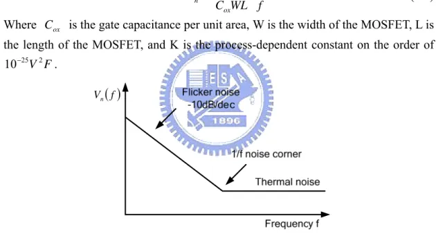
(20) Chapter 2 Dynamic Offset Cancellation Techniques. buried channel of PMOS. So, PMOS introduces less flicker noise than NMOS.. Vn2 ( f ) =. 1 K ⋅ C oxWL f. I d2 ( f ) = 4kTγg m. Figure 2-5 MOSFET noise model, including flicker noise voltage source and thermal noise current source. Vn2 =. K 1 ⋅ . CoxWL f. (2.3). Where Cox is the gate capacitance per unit area, W is the width of the MOSFET, L is the length of the MOSFET, and K is the process-dependent constant on the order of. 10 −25V 2 F . Vn ( f ). Figure 2-6 Noise spectrum of the MOSFET The total noise voltage of the MOSFET can be written as Vn2 =. ⎛2 1 ⎞ K 1 ⎟⎟. ⋅ + 4kT ⎜⎜ ⋅ CoxWL f ⎝ 3 gm ⎠. (2.4). Figure 2-6 shows the noise power spectrum. There is an intersection point between flicker noise and thermal noise. It is called “corner frequency” or “1/f noise corner”. It happens when the flicker noise power is equal to the thermal noise power. The equation can be derived as. -8-.
(21) Chapter 2 Dynamic Offset Cancellation Techniques. ⎛2 1 ⎞ K 1 ⎟⎟. ⋅ = 4kT ⎜⎜ ⋅ CoxWL f c ⎝ 3 gm ⎠. (2.5). The 1/f noise corner is derived as fc =. K 3 ⋅ ⋅ gm . CoxWL 8kT. (2.6). 2.3 Dynamic Offset Cancellation Techniques Many bio-chips or sensor ICs deal with the signals in millivolt range. However, in CMOS IC technology, the offset of ordinary analog integrated circuits are also in millivolt range. Therefore, IC designers have developed many ways to reduce the offset. There are three common solutions. First, one can use larger devices with certain layout technique. The process variation and lithographic errors cause the mismatch of the differential pairs and introduce the offset. According to the mismatch model (2.7), the mismatch of the threshold voltage is inversely proportional to the device area.. Where AVt. AVt2 σ (ΔVt ) = . W ⋅L is the mismatch parameter (mV/μm).. (2.7). Nevertheless, larger device area means higher cost. Second, one can use laser trimming. But, it needs extra test infrastructures. Third, one can use dynamic offset cancellation techniques. The last one is preferable to others for excellent long term stability and moderate costs. The following sections introduce auto-zeroing and chopping techniques.. Auto-zero Amplifier (AZA) Figure 2-7 shows an auto-zeroing (AZ) example. There are two modes of operation: an auto-zero phase and an amplification phase. In the auto-zero phase ( φ =1), the amplifier samples the offset and then store on the capacitor. After settling, the offset on the capacitor is VOS ⋅. A . In the amplification phase ( φ =0), the output A +1. signal is available. Since the flicker noise and offset is highly correlated with the next sample, it can be subtracted from the amplified input signal. Finally, the offset at the output is. VOS . A +1 -9-.
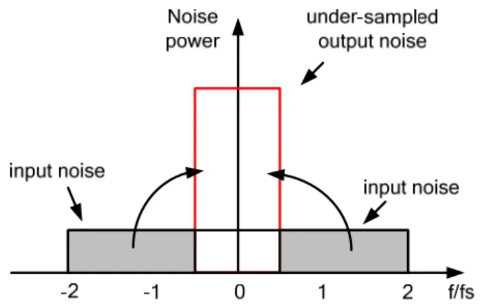
(22) Chapter 2 Dynamic Offset Cancellation Techniques. φ φ. φ. Figure 2-7 Auto-zeroing technique. vn ,i. vn ,o S/H circuit. Figure 2-8 Auto-zeroing concepts Conceptually, the system behavior is shown in Figure 2-8. Let H(f) be the transfer function of S/H circuit, and the noise transfer function is vn ,o ( f ) = vn ,i ( f ) ⋅ (1 − H ( f )). We know that Since (1 − H ( f )). (2.8). H ( f ) = sin c( f ).. (2.9) is a high-pass transfer function, the offset and 1/f noise can be. reduced. However, the disadvantage of AZ is the noise fold-over. Figure 2-9 and 2-10 illustrate the phenomenon. If there is input noise frequency higher than Nyquist rate, the under-sampled output noise will be folded over to DC.. Figure 2-9 Out of band input noise is folded over to DC. - 10 -.
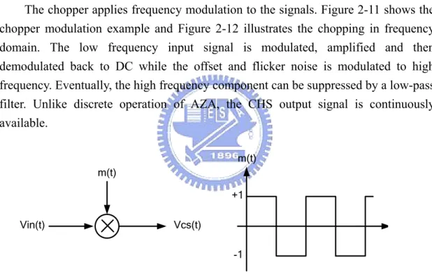
(23) Chapter 2 Dynamic Offset Cancellation Techniques. Vn ( f ). Before AZ After AZ. Vn, AZ ( f ). Frequency f. Figure 2-10 Residual noise of AZ impacts on the noise spectrum. Chopper-Stabilized (CHS) Amplifier The chopper applies frequency modulation to the signals. Figure 2-11 shows the chopper modulation example and Figure 2-12 illustrates the chopping in frequency domain. The low frequency input signal is modulated, amplified and then demodulated back to DC while the offset and flicker noise is modulated to high frequency. Eventually, the high frequency component can be suppressed by a low-pass filter. Unlike discrete operation of AZA, the CHS output signal is continuously available. m(t) m(t) +1 Vin(t). Vcs(t) -1. Figure 2-11 The input signal Vin(t) is multiplied by carrier signal m(t) and transposed to a higher frequency where is no flicker noise.. - 11 -.
(24) Chapter 2 Dynamic Offset Cancellation Techniques. Figure 2-12 CHS in frequency domain If the chopping frequency is much larger than corner frequency and the amplifier is ideal, the flicker noise is removed completely after chopping. Figure 2-13 shows the noise spectrum of CHS.. Vn ( f ). Vn,CHS ( f ). Before CHS. After CHS. Frequency f. Figure 2-13 Residual noise of CHS On the subject of time domain analysis, given a DC input signal and infinite amplifier bandwidth, the modulated signal is a square wave. In practical, the amplifier bandwidth is finite and it needs settling time. Figure 2-14 shows the difference. The actual demodulated DC signal is less than ideal one. Thus, the limited amplifier bandwidth reduces the effective gain (2.10).. (. Aeff = Anom 1 − 4 τ - 12 -. T. ).. (2.10).
(25) Chapter 2 Dynamic Offset Cancellation Techniques. Where f ch = 1 and ω−3dB = 1 . For example, if the amplifier bandwidth is ten T τ times the chopping frequency, the gain error is about 6.37%. 4. π. ⋅ A ⋅ Vin. 8. π2. ⋅ A ⋅ Vin. Figure 2-14 CHS in time domain. Figure 2-15 Spikes and the residual offset due to finite bandwidth The charge injection of the switches at the input chopper introduces spikes. After filtering, the spikes become the DC component of the signal. It is residual offset of the chopper amplifier. The magnitude of the residual offset can be derived as Residual offset = 2f ch Vspike τ.. (2.11). Where f ch is the chopping frequency, Vspike is the spike magnitude, and τ is the. - 13 -.
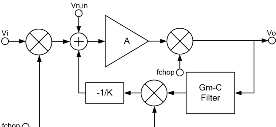
(26) Chapter 2 Dynamic Offset Cancellation Techniques. settling time constant. In a low supply voltage environment, the residual offset is crucial. To reduce the residual offset, the smaller settling time constant and low chopping frequency are preferred. However, at a given residual offset, the smaller settling time constant means more power consumption and low chopping frequency has more 1/f noise component. Thus, a trade-off between power and performance is required here.. 2.4 AC Coupled Chopper-Stabilized Amplifier with AC feedback circuits For biomedical applications, the conventional chopper-stabilized amplifiers or auto-zero amplifiers cannot satisfy the requirements. There are three problems. The first one is on the difference of the electrode common-mode voltage and the circuits input common-mode voltage. The electrodes common-mode voltage varies with time and is even lower than the earth ground. Using two chopper-stabilized amplifiers with nMOS and pMOS input pairs achieve rail-to-rail input stage [7]. However, it requires two power supply and extra area overhead. The modern solution is the one of AC coupled input stage. It blocks the common-mode signal and let differential signals go through. The second one is differential electrode offset (DEO) issue. For conventional Ag/AgCl electrodes, the DEO is as high as 50mV and varies with time. Because the chopper-stabilized amplifier is inherently DC coupled system, DEO may causes the amplifier to saturate and be out of operation point. Thus, a high-pass filter is required before amplification. Using external passive components before amplifier or differential difference amplifier with resistive feedback circuits are ways to solve DEO. However, the former degrades the signal-to-noise ratio (SNR) and the latter consumes excessive power. Here, an AC feedback circuits filters the DEO without extra costs. Figure 2-16 shows the proposed architecture. It consists of a capacitive closed-loop chopper-stabilized amplifier with a DC gain A, a Gm-C filter, and an AC feedback circuits with a loop gain 1/K. Before going through the system, the input signal is modulated and transposed to high frequency before the 1/f noise is mixed. After amplification, the noise is modulated to high frequency. Since the signal is modulated twice, the output signal is demodulated back to low frequency signal. If there is a DEO at the input electrodes, the amplifier enters into the saturation region and output goes up to VDD or VSS. At the moment, the Gm-C filter integrates the output signal, extracts the DC component and then feedback to the system and cancel the DEO. Eventually, the system is back to the operation point.. - 14 -.
(27) Chapter 2 Dynamic Offset Cancellation Techniques Vn,in. Vi. Vo. A. fchop. Gm-C Filter. -1/K. fchop. Figure 2-16 AC Coupled Chopper-Stabilized Amplifier with AC feedback circuits block diagrams. The transfer function can be derived as H (s ) =. 1 Vo (s ) = A⋅ Vi (s ) 1+ s. ⋅. ω LP. 1. 1+. ω HP. .. (2.12). s. If 1/K is finite, the output offset to input offset transfer function is obtained as Vo ,DC = Vi ,DC ⋅. A 1+ A. .. (2.13). K. The output noise is finally transposed to high frequency. It is derived as 2. 2 ⎛ 2 ⎞ +∞ 1 S n ,out ( f ) = ⎜ ⎟ ⋅ ∑ 2 A( f − n ⋅ f chop ) ⋅ S n ,in ( f − n ⋅ f chop ). (2.14) ⎝ π ⎠ n=−∞ n n odd. It is evident that the system has a band-pass characteristic. It blocks DEO and suppresses unwanted high frequency noise.. 2.5 Summary In order to deal with the bio-potentials, the low noise analog front-end amplifier plays an important role. Apparently, the AZA only reduces flicker noise, without limiting the amplifier bandwidth; the CHS eliminates the flicker noise, but limits the amplifier bandwidth. However, the conventional CHS is a DC coupled system and unable to handle the biomedical signals for DEO and different common-mode voltage issues. Thus, an AC coupled chopper-stabilized amplifier with AC feedback circuits is proposed. The architecture blocks a DEO and tolerates the electrodes common-mode voltage variance. - 15 -.
(28) Chapter 3 Fundamentals of Low-Voltage Low-Power SAR ADC. Chapter 3 Fundamentals of Low-Voltage Low-Power Successive Approximation Register Analog-to-Digital Converter. 3.1. Introduction. In general, the signal process is preferred to be done with digital approaches than analog ones. Because digital signal processor (DSP) has large noise margin and is insensitive to circuit imperfection. Furthermore, powerful DSP is able to perform complex algorithms or execute programs. The natural signals are continuous-time analog, so an analog-to-digital converter (ADC) is essential. The quality of the digital signals depends on the ADC performance. Nevertheless, there are many non-ideal factors, such as quantization error, thermal noise and non-linearity, degrades the ADC performance. The design issues are more crucial for low voltage circuits. In this chapter, an low voltage low-power successive approximation register (SAR) analog-to-digital converter is stated. Section 3.2 introduces the SAR ADC based on charge redistribution approach. Section 3.3 describes the modern low-voltage design techniques. Section 3.4 presents the proposed SAR ADC circuits. Section 3.5 states the SAR implementation in CMOS technology. Section 3.6 makes a brief summary of this chapter.. - 16 -.
(29) Chapter 3 Fundamentals of Low-Voltage Low-Power SAR ADC. 3.2. Successive Approximation Register. Analog-to-Digital Converter Based on a Charge Redistribution Principles The major advantage of SAR ADC is simple and low power. Because the SAR ADC does not need opamp, it is a preferable architecture for low-speed medium-resolution application. Figure 3-1 describes the SAR ADC concepts. The conventional SAR ADC consists of a digital-to-analog converter (DAC), a comparator and a SAR. The basic principle is that the DAC produces a voltage and then does the binary search for the input voltage. Therefore, it requires at last N conversion cycles for N-bit resolutions.. Figure 3-1 SAR ADC architecture. - 17 -.
(30) Chapter 3 Fundamentals of Low-Voltage Low-Power SAR ADC. VDD. Sx. VDAC. 2 N −1 C. 2 N −2 C. 2 N −3 C. S N −1. S N −2. S N −3. 21 C. 20 C. 20 C. S1. S0. St Vref. Si Vi. Figure 3-2 Charge-redistribution SAR ADC. Theoretically, it needs N+1 conversion cycles for N-bit resolutions. The additional conversion cycle initiates all registers and resets the comparators. Figure 3-2 shows the general SAR ADC based on charge-redistribution architecture. The total capacitance for N-bit DAC is derived as N −1. Ctotal = ∑ 2i ⋅ C + 2 0 ⋅ C = 2 N ⋅ C.. (3.1). i =0. Assume AGND stands for analog ground, Vi represents the input signal, and Vref is the reference voltage. There are three modes of operations: Sample, hold and redistribution. 1.. 2.. Sample Mode z. S x is switched to AGND. z. S i is switched to Vi. z. S t , S 0 , S1 , S N −1 are switched to Vi. z. VDAC = 0. Hold Mode z. S x open. z. S t , S 0 , S1 , S N −1 are switched to AGND - 18 -.
(31) Chapter 3 Fundamentals of Low-Voltage Low-Power SAR ADC. z. 3.. VDAC = −Vi. Redistribution Mode z. S i is switched to Vref. z. Binary search, resolve one bit at a time. Starting with MSB bN −1. z. Bit bN −1 conversion. z. . S N −1 is switched to Vref. . VDAC = −Vi +. . If VDAC <0, bN −1 =1, S N −1 → Vref. . If VDAC >0, bN −1 =0, S N −1 →AGND. V 2 N −1 ⋅ C ⋅ Vref = −Vi + ref 2 Ctotal. Bit b j conversion, j=N-2, N-3,…,0 . S j is switched to Vref. . VDAC = −Vi +. Vref 2N. ⋅. 2j ⋅C ⋅ Vref Ctotal. N −1. ∑ bk ⋅ 2k +. k = j +1. . If VDAC <0, b j =1, S j → Vref. . If VDAC >0, b j =0, S j →AGND. Eventually, VDAC is represented as VDAC = −Vi +. Vref 2N. N −1. ⋅ ∑ bi ⋅ 2i .. In order to avoid leakage of S x , the analog ground is set to VDD input range is from VDD. 2. (3.2). i =0. 2. and the. to VDD . And switches are implemented as CMOS. switches. After conversion, in ideal case, VDAC is close to Vi and the difference should be smaller than half of the least significant bit (LSB). However, comparator’s finite bandwidth, noise and the parasitic effect degrades the ADC performance. Next, the analyses of quantization noise and capacitor mismatch are stated. - 19 -.
(32) Chapter 3 Fundamentals of Low-Voltage Low-Power SAR ADC. Quantization Noise Analysis The function of ADC is basically a quantization process. The continuous-time input signal x(t ) is converted to discrete-time signal x(k ) and then quantized to digital signal y (k ) . Figure 3-3 describes the ADC quantization process model and its linear model.. x(k ). x(t ). y (k ). S&H Quantizer. q (k ). y (k ). x(k ). Figure 3-3 Quantizer linear model The quantization noise is represented as q (k ) ≡ y (k ) − x(k ).. (3.3). Noise power is derived as. Pn = ∫ q 2 ⋅ pdf (e ) ⋅ dq =. 1 2 ⋅Δ . 12. (3.4). Where pdf represents the probability density function, shown in Figure 3-4 and Δ is the difference between two adjacent quantization levels. −Δ. Δ. 2. q. 2. Figure 3-4 PSD of the quantization noise Assume that the quantization noise q (k ) uniformly distributes within the Nyquist - 20 -.
(33) Chapter 3 Fundamentals of Low-Voltage Low-Power SAR ADC. frequency. Let f s be the sampling frequency, f i is the input signal frequency, input x (k ) is the sinusoidal wave with an amplitude A. 2πf k ⎞ x(k ) = A ⋅ sin ⎛⎜ i . f s ⎟⎠ ⎝. (3.5). Signal power is derived as Ps =. 1 2 ⋅A . 2. (3.6). (3.6) divided by (3.4), the signal-to-noise ratio (SNR) is obtained as SNR =. Ps A2 = 6⋅ 2 . Pn Δ. (3.7). If input signal amplitude A is the half of the full scale amplitude, SNR is rewritten as SNR =. 3 2N ⋅ 2 = 6.02 ⋅ N + 1.76dB. 2. (3.8). Thus, in order to obtain the highest SNR, the input signal is demanded to be amplified as large as possible.. Capacitor Mismatch Analysis and Parasitic Effect The performance depends on the accuracy of DAC. It is composed of passive components, such as capacitors or resistors. Unfortunately, metal or temperature gradient variation causes a component mismatch problem. According to the mismatch model (3.9), the mismatch of the capacitors is inversely proportional to the device area. Thus, there is a trade-off between cost and accuracy. In general, the charge-redistribution DAC with a resolution over 10bits requires calibrations or trimming.. σ (ΔC ) C. =. AC . W ⋅L. For a charge-redistribution DAC, the output voltage is N −1 C VDAC = Vref ⋅ N ⋅ ∑ bi ⋅ 2i . 2 ⋅ C + C p i =0. (3.9). (3.10). If there is a capacitor mismatch, the DAC output voltage has an error and. - 21 -.
(34) Chapter 3 Fundamentals of Low-Voltage Low-Power SAR ADC. introduces differential non-linearity (DNL) and integral non-linearity (INL). INL is derived as. (. ). INL max = 2 N −1 ⋅ C + ΔC max,INL − 2 N −1 ⋅ C = 2 N −1 ⋅ ΔC max,INL .. (3.11). Where C is the unit capacitance and the maximum ΔC that will result in an INL which is less than 1 ⋅ LSB is 2 ΔC max,INL =. C . 2N. (3.12). DNL is defined by DNLmax = (2 N − 1) ⋅ ΔC max,DNL .. (3.13). With the maximum ΔC , which leads to a DNL less than 1 ⋅ LSB is 2 ΔC max,DNL =. C. 2. N +1. −2. .. (3.14). Besides, the parasitic capacitance causes gain error. Higher resolution requires larger capacitance and more area to reduce the mismatch. It leads to more severe parasitic effect and requires higher comparator gain. Thus, there is a trade-off bewteen accuracy and power.. 3.3. The Proposed 11-b Low-Voltage. Low-Power SAR A/D converter Under the low supply voltage environment ( Vthp + Vthn > VDD ), there are many design challenges. For the conventional SAR ADC, there are two problems. First, CMOS switches cannot work efficiently. If input voltage is at the middle of the supply voltage, neither NMOS nor PMOS is unable to turn on. Second, input range is limited to half of the full scale voltage. In order to solve the problem, the novel low-voltage SAR ADC is presented. The conventional successive approximation algorithm uses a DAC to binary search the input voltage. The proposed algorithm is adds or subtracts by the DAC voltage to binary search. VDD. 2. . It is shown in Figure 3-5. There are two advantages.. First, it achieves rail-to-rail input range without a rail-to-rail comparator. Second, it adopts a grounded-switches technique. It means all switches are only switched to - 22 -.
(35) Chapter 3 Fundamentals of Low-Voltage Low-Power SAR ADC. VDD or VSS . Thus, it is easy to provide adequately low switch on-resistance.. Figure 3-5 Proposed SAR ADC architecture. VREF = VDD. VDD. 2. Sh. Vi. 210 C 29 C 28 C 27 C 26 C 25 C 2 4 C 23 C 22 C 21 C 20 C. VDD VSS. Figure 3-6 A 11-bit low-power and low-voltage SAR ADC Because the front-end amplifier has a 70dB dynamic range (DR), a 11-bit SAR ADC is integrated. It is shown in Figure 3-6. The switch S h is bootstrapped. It provides a rail-to-rail input range. And the others switches are grounded-switches. The switching operations are controlled by the successive approximation register (SAR). The whole operation is as follows. Let N=10, i=0 z. Sample mode Sh close S10 → VDD , S0-S9 → VSS - 23 -.
(36) Chapter 3 Fundamentals of Low-Voltage Low-Power SAR ADC. z. Hold mode Sh open test bN . z. Comparator activated and compared VDAC with VDD. 2. Redistribution mode ( i conversion cycle) As clk 0->1. . . If VDAC > V DD 2 , bN −i =1, bN −i → VSS. . If VDAC < VDD. . Comparator reset i=i+1, test bN −i → VDD. 2. , bN −i =0, bN −i → VDD. As clk 1->0 . Comparator activated and compared VDAC with VDD. Finally, the DAC output voltage VDAC is close to VDD. 2. 2. . It is represented as.. 10. b VDAC = Vin + ∑ (− 1) N −i ⋅ VDD i =0. 2i+2. .. (3.15). Comparator The comparator plays an important role in SAR ADC. In order to minimize the power consumption, there is only one current branch in this design. The comparator is shown in Figure 3-7. It includes a preamplifier and a latch. The configuration has three advantages. First, a weak-inversion input pair maximize the. gm. ID. ratio.. Second, PMOS input pairs have less flicker noise than NMOS. It is good for low-speed applications. Third, the source and the body of the PMOS is tied together to reduce threshold voltage mismatch and avoid body effect. It also enhances the common-mode immunity and input common-mode range.. - 24 -.
(37) Chapter 3 Fundamentals of Low-Voltage Low-Power SAR ADC. Figure 3-7 Latched comparator The operation of the comparator is straightforward. There are two phases of operations. During the “reset” phase, M3 and M4 discharge the output nodes. In the phase, the comparator output is not available. The “compare” phase activates the latch and compares the difference. After settling, the comparator output is available. To determine current and transistor size, the analysis is as follows. . In “compare” phase. Given a voltage difference ΔV , the ouptut function of time t is represented as Vout (t ) = ΔV ⋅ e τ . t. (3.16). Let t a be the conversion period. The output is required to settle before the time ends. Vout (t a ) = ΔV ⋅ e. Where the settling time constant τ = C. ta. τ. ≥ VDD .. g m5. (3.17). and it is has to be ( N + 1) ⋅ ln 2 times. more than conversion period t a ta. . ⎛VDD ⎞ = (N + 1) ⋅ ln 2. ΔV ⎟⎠ τ = ln⎜⎝. (3.18). In “reset” phase. The transistors M3 and M4 are fully turn on. Their resistance is represented as R= 1. g m3. .. (3.19). Considering the overdrive recovery issue. Assume the comparator is saturated and the. - 25 -.
(38) Chapter 3 Fundamentals of Low-Voltage Low-Power SAR ADC. clock becomes high at t=0. If there is a input signal ΔV = 1 ⋅ LSB . The output 2 function of time t is derived as −t Vout (t ) = ( A ⋅ ΔV + I ⋅ R ) ⋅ ⎛⎜1 − e τ ⎝. ⎞⎟ − I ⋅ R. ⎠. (3.20). Where A is the comparator gain during “reset” phase, I represents the comparator tail current and τ stands for the ouput node time constant. The recovery time is defined by − tre cov ery ⎛ τ ⎞ Vout (t re cov ery ) = ( A ⋅ ΔV + I ⋅ R ) ⋅ ⎜1 − e ⎟ − I ⋅ R = ΔV . ⎝ ⎠. (3.21). ⎡ A ⋅ ΔV + I ⋅ R ⎤ ⇒ t re cov ery = RC ⋅ ln ⎢ (3.22) ⎥. ⎣ ( A − 1) ⋅ ΔV ⎦ In order to minimize the recovery time, it needs a high bandwidth and high gain comparator. However, higher bandwidth means more power consumption. Thus, there is a trade-off between speed and power.. Figure 3-8 Given a input sequence {+0.5VDD, +0.25LSB, +0.5VDD, -0.25LSB, -0.5VDD, +0.25LSB, -0.5VDD, -0.25LSB }, the simulated output sequence={1, 1, 1, 0, 0, 1, 0, 0} under five corner cases (FF, FS, TT, SF, SS). Clock rate=32KHz. Thermal Noise Due to the MOS resistance and parasitic resistance, there is a thermal noise at the DAC output during conversion. The resistive thermal noise can be modeled as a noiseless resistor series with a noise source. Thus, the equivalent model is shown in. - 26 -.
(39) Chapter 3 Fundamentals of Low-Voltage Low-Power SAR ADC. Figure 3-9 for the MSB conversion cycle. Since MSB capacitor is connected to VDD and the other capacitors are switched to VSS , the equivalent capacitance is 2 9 ⋅ C . Thus, the thermal noise is derived as 1 KT < ⋅Δ 9 2 ⋅C 2. (3.23). Where K is the Boltzmann constant, T is the absolute temperature, and Δ represents a LSB. Vi. vns2. VDAC. 210 C. 210 C. vn22. vn21. Figure 3-9 Thermal noise models as testing MSB VDAC. (2. 10. ). + 29 C. 29 C. vn22. vn21. Figure 3-10 Thermal noise models during the next conversion after MSB KT <Δ 384 ⋅ C. (3.24). In next conversion cycle, the thermal noise is modeled as shown in Figure 3-10. It shows the capacitance requirement is looser than the MSB. Thus, the thermal noise power is largest during MSB conversion. If it satisfies the requirement, the other bit - 27 -.
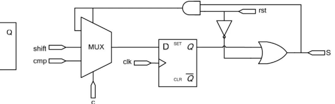
(40) Chapter 3 Fundamentals of Low-Voltage Low-Power SAR ADC. conversions will satisfy as well. In general, the thermal noise power should be less than the quantization noise power. Therefore, the unit-capacitance is known.. Voltage multiplier For a low power supply, the conventional CMOS sampling switch is unable to offer adequate low switch-on resistance. In order to achieve the rail-to-rail input range, the bootstrapped technique is adopted. The sampling switch is implemented as NMOS switch. It is driven by the boosted clock driver shown in Figure 3-11. By the source and gate cross-coupled of M1 and M2 configuration, the capacitor C1 and C2 are charged alternatively. In steady state, the voltage drop across the capacitor C1 and C2 is VDD . When the input clock becomes high, the output voltage is boosted to 2V DD . As the clock is low, M4 is turned on and the output is pull down to VSS . Actually, the boosted output voltage cannot reach 2VDD for the parasitic effect and charge sharing. In order to reduce the effect, capacitor C1 and C2 must be sufficiently large. Thanks for the light loading of the small sampling switch and the low speed clock rate, the power consumption of the boosted clock driver is as low as ten nano-watt of magnitude.. VDD 2 ⋅ VDD M1. M2. clock. out. M3. VDD C1. C2. M4. Figure 3-11 Boosted clock driver. 3.4. Successive Approximation Register (SAR). In this thesis, a CMOS successive approximation register is implemented. It is. - 28 -.
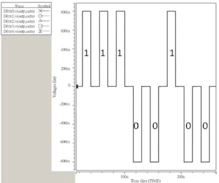
(41) Chapter 3 Fundamentals of Low-Voltage Low-Power SAR ADC. composed of MUX, D flip-flop and simple logic circuits. In order to save the area, all transistors are of minimal size. All blocks are also implemented as standard cells. The sequential digital circuit is realized as a finite state machine shown in Table 3-1. A 11-bit SAR ADC requires 12 conversion cycles. During the first conversion cycle, SAR ADC samples the input signal and resets all registers. Note that the control signal S10 is reset to logic ‘1’. In second conversion cycle, the sampled signal is held. After settling, the comparator is activated and the first bit is extracted. The other conversion cycles are similar. Table 3-1 SAR operation Conversion SAR output control signals Cycle. Cmp result. S10. S9. S8. S7. S6. S5. S4. S3. S2. S1. S0. 1. 1. 0. 0. 0. 0. 0. 0. 0. 0. 0. 0. -. 2. 1. 0. 0. 0. 0. 0. 0. 0. 0. 0. 0. D10. 3. D10 1. 0. 0. 0. 0. 0. 0. 0. 0. 0. D9. 4. D10 D9 1. 0. 0. 0. 0. 0. 0. 0. 0. D8. 5. D10 D9 D8 1. 0. 0. 0. 0. 0. 0. 0. D7. 6. D10 D9 D8 D7 1. 0. 0. 0. 0. 0. 0. D6. 7. D10 D9 D8 D7 D6 1. 0. 0. 0. 0. 0. D5. 8. D10 D9 D8 D7 D6 D5 1. 0. 0. 0. 0. D4. 9. D10 D9 D8 D7 D6 D5 D4 1. 0. 0. 0. D3. 10. D10 D9 D8 D7 D6 D5 D4 D3 1. 0. 0. D2. 11. D10 D9 D8 D7 D6 D5 D4 D3 D2 1. 0. D1. 12. D10 D9 D8 D7 D6 D5 D4 D3 D2 D1 1. D0. The whole block diagram of SAR is described in Figure 3-14 and the block details are shown in Figure 3-12 and Figure 3-13. It bahaves like a series shift register. When the global reset signal asserts, S10 is reset to ‘1’ and S0-S9 are reset to ‘0’. As the conversion starts , the logic ‘1’ is passed to the next block sequentially. After the conversion finishes, the global reset signal asserts again. All blocks and logic circuits are implemented as standard cells with minimial size.. - 29 -.
(42) Chapter 3 Fundamentals of Low-Voltage Low-Power SAR ADC. Figure 3-12 The first bit logic block of SAR Table 3-2 The mux output versus the first control signal S c. Mux output. 0. 0 Shift. 0. 1 S. 1. 0 cmp. 1. 1 S. Figure 3-13 The other bit logic blocks of SAR Table 3-3 The mux output versus the rest control signal S c. Mux output. 0. 0 Shift. 0. 1 S. 1. 0 cmp. 1. 1 S. - 30 -.
(43) Chapter 3 Fundamentals of Low-Voltage Low-Power SAR ADC. Figure 3-14 Successive approximation register architecture - 31 -.
(44) Chapter 3 Fundamentals of Low-Voltage Low-Power SAR ADC. Given an ideal comparator and capacitor array, the SAR simulation result is shown in Figure 3-15. The input signal 0 and VDD are tested. Because the conversion results are the complements of the control signals in the thesis, the extracted bits are ‘000 0000 0000’ and ‘111 1111 1111’. rst Vi S10 S9 S8 S7 S6 S5 S4 S3 S2 S1 S0. Figure 3-15 SAR simulation results. 3.5. Simulation Results. Given a 402.7Hz 0.6Vp-p input sinusoidal signal, FFT simulation is shown in Figure 3-16. It has a SNR of 63.6dB, a SNDR of 63dB and a SFDR of 72.6dB. The power consumption is 0.31μW excluding the bias current. The clock rate is 32 KHz and the conversion rate is 2.67 KS/s. The supply voltage is 0.8V. Table 3-4 is the total corner simulation results. Because the threshold voltage is as high as 0.5V in the SS corner, it degrades the performance significantly. Figure 3-17 and Figure 3-18 are the simulated INL and DNL at the TT corner cases. Both of them are smaller than a LSB.. - 32 -.
(45) Chapter 3 Fundamentals of Low-Voltage Low-Power SAR ADC. Figure 3-16 FFT simulation in TT corner @402.7Hz input signal and 0.6Vp-p swing Table 3-4 SAR ADC performance versus different corner cases Corner. TT. FF. SS. SNR. 63.6dB. 63.4dB. 53.1dB. SNDR. 63dB. 62.4dB. 52.6dB. ENOB. 10.18b. 10.08b. 8.45b. SFDR. 72.6dB. 69.7dB. 64. 7dB. Figure 3-17 INL simulation in TT corner @402.7Hz input signal and 0.6Vp-p swing - 33 -.
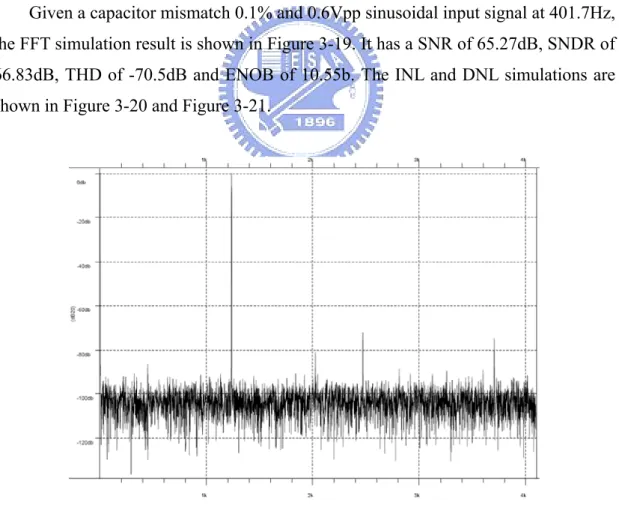
(46) Chapter 3 Fundamentals of Low-Voltage Low-Power SAR ADC. Figure 3-18 DNL simulation in TT corner @402.7Hz input signal and 0.6Vp-p swing Given a capacitor mismatch 0.1% and 0.6Vpp sinusoidal input signal at 401.7Hz, the FFT simulation result is shown in Figure 3-19. It has a SNR of 65.27dB, SNDR of 66.83dB, THD of -70.5dB and ENOB of 10.55b. The INL and DNL simulations are shown in Figure 3-20 and Figure 3-21.. Figure 3-19 FFT simulation in TT corner @401.7Hz input signal and 0.6Vp-p swing with 0.1% capacitor mismatch. - 34 -.
(47) Chapter 3 Fundamentals of Low-Voltage Low-Power SAR ADC. Figure 3-20 INL simulation in TT corner @401.7Hz input signal and 0.6Vp-p swing with 0.1% capacitor mismatch. Figure 3-21 DNL simulation in TT corner @401.7Hz input signal and 0.6Vp-p swing with 0.1% capacitor mismatch With a capacitor mismatch 0.1%, it leads to larger INL and DNL. It has a DNL of ± 1.15LSB. and an INL of ± 1.085LSB. Nevertheless, the ENOB is above 10-b and. satisfies the requirements.. - 35 -.
(48) Chapter 3 Fundamentals of Low-Voltage Low-Power SAR ADC. Table 3-5 SAR ADC performance. 3.6. Spec.. @fin=402.67Hz. # bits. 11. VDD. 0.8V. Pd (AVG). 0.31μW. SFDR. 72.6 dB. SNR. 63.6 dB. SNDR. 63 dB. ENOB. 10.18b. DNL. < ±0.96LSB. INL. < ±1LSB. Fs. 2.67 KS/s. Input range. 0.6V. Technology. 0.18μm. Summary. The proposed SAR ADC has a SNDR of 63dB in a low supply voltage of 0.8V and power consumption of 0.31μW. It adopts the novel successive approximation algorithm and grounded-switches techniques. The former achieves a rail-to-rail input common-mode range without a rail-to-rail input comparator. The latter provides sufficient low switch on-resistance. Besides, there is no opamp and only one current source in the whole architecture, so the power consumption is low.. - 36 -.
(49) Chapter 4 A 0.8-V Low-Power Analog Front-End IC for Biomedical Applications. Chapter 4 A 0.8-V Low-Power Analog Front-End IC for Biomedical Applications. 4.1. Introduction. This chapter describes a 0.8-V low-power bio-potential readout front-end IC. Section 4.2 introduces the whole IC specification and design. Section 4.3 states the instrumentation amplifier and simulations. Section 4.4 presents the programmable gain amplifier and simulations. Section 4.5 includes the simulation results and the target spec. Section 4.6 states the measurement considerations. Section 4.7 presents the measurement results and the performance summary. Section 4.8 states the comparison with the state of the art.. 4.2. AFE IC Design. The Proposed Digitally Programmable AFE IC Figure 4-1 shows the proposed biomedical analog front-end (AFE). The skin electrodes Kendall H99SG provides the interface between body and the circuits. The instrumentation amplifier amplifies the signal while rejects common-mode noise. In order to accommodate different bio-potentials, the programmable gain amplifier offers - 37 -.
(50) Chapter 4 A 0.8-V Low-Power Analog Front-End IC for Biomedical Applications. a variable gain controlled by digital interface. Finally, the 11-b SAR ADC converts the analog signal to digital signal.. Gain. Bandwidth. Digital Interface. Cext. IA. PGA. 11-b SAR ADC. 11. 11-to-1 MUX. Figure 4-1 The proposed AFE IC. Design specifications The specifications of the amplifier are listed in Table 4-1. In order to realize a long-term monitoring portable bio-potential acquisition IC, the supply voltage is chosen as low as 0.8V. It is low supply voltage poses lots of design challenges. Power budget upper bound is 5μW to ensure a lifetime of more than one year. The voltage gain has to be as large as possible for better data conversion. However, the limited voltage headroom in such low supply environment, the distortion issue is vital. Common-mode rejection ratio (CMRR) is the one of the most important issues in bio-potential acquisition analog front-end. Because a large 50/60Hz common-mode disturbance corrupts the signal quality, it needs a very high CMRR to purify the signal. According to International Federation of Clinical Neurophysiology (IFCN), CMRR must be at least 110dB for each channel. The total harmonic distortion (THD) must be less than 1%. According to dynamic range definition, the effective dynamic range is the largest input signal with THD<1% over the input-referred noise within the signal bandwidth. Thus, it is essential to make sure THD<1% for dealing with any biomedical signal. In order to obtain a 10-bit SNR, the dynamic range has to be over than 60dB. Besides, the noise performance is the key performance of the front-end amplifier. It determines the SNR. From Table 1-1, the input-referred noise should be less than 1μVrms for a 10-bit SNR. - 38 -.
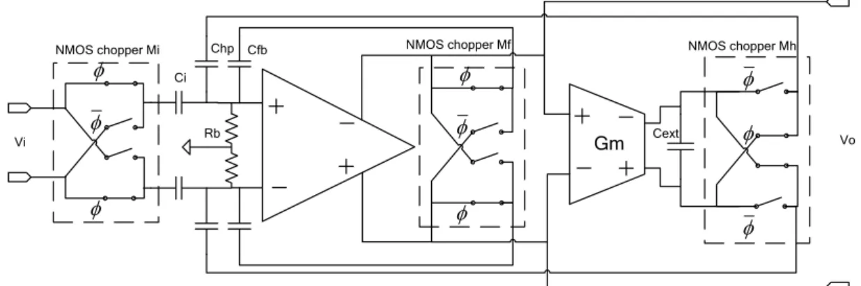
(51) Chapter 4 A 0.8-V Low-Power Analog Front-End IC for Biomedical Applications. Table 4-1 Specification of the front-end amplifier Spec.. Value. Unit. Supply voltage. 0.8. Volt. Power consumption <5. μW. Gain. >40. dB. CMRR. 110. dB. THD. <1. %. Dynamic range. >60. dB. Input-referred noise 1 Bandwidth. 4.3. μVrms (0.5Hz to 100Hz). 0.5-100,400 Hz (programmable). Instrumentation Amplifier. The concept of the AC coupled chopper-stabilized amplifier with AC feedback circuits is shown in Figure 2-16 and (2.12) derives the system transfer function. Figure 4-3 shows the simplified schematic. It includes a fully-differential folded-cascode opamp, a gm-c filter, three NMOS chopper and capacitors. Since the CMOS chopper is unable to work at a low supply voltage environment, the bootstrapped NMOS chopper is adopted without reliability issue. There are two feedback paths in the system. One is for setting the closed-loop gain and the other is for cancelling DEO. The capacitive closed-loop configuration dissipates less power than the resistive feedback one. Note that the demodulation of the signal is inside the opamp. The transfer function is presented as C 1 1 1 v (s ) H(s ) = o . ⋅ ⋅ = i ⋅ vi (s ) C C C C C s ω + + + 1 i fb hp p 1+ HP fb 1 + 1+ ⋅ ω LP s Ao C fb. (4.1). The low-pass cutoff frequency is derived as. ω LP = ωt ⋅. C fb Ci. .. (4.2). And the high-pass cutoff frequency is derived as. ω HP =. Ci Chp Gm ⋅ ⋅ . C fb C fb C. - 39 -. (4.3).
(52) Chapter 4 A 0.8-V Low-Power Analog Front-End IC for Biomedical Applications. φ. φ. φ Figure 4-2 NMOS chopper The midband gain is set by C hp. Ci. C fb. and the DEO cancelling loop gain is set by 2. C fb. . Let the amplifier thermal noise be v ni , the closed-loop input-referred noise. is derived as 2. vni ,cl. 2. ⎛ C + C fb + Chp + C p ,i ⎞ ⎟⎟ ⋅ vni 2 . = ⎜⎜ i Ci ⎝ ⎠. (4.4). In order to reduce the thermal noise, the input capacitance C i should be chosen as large as possible. But it increases the chip area and parasitic capacitance. Thus, there is a trade-off between the performance and area. In this thesis, the midband gain is set to be a little larger than 40dB to attenuate the parasitic effect. The input capacitance C i is 16pF, the feedback capacitance C fb is 0.15pF and the DEO feedback capacitance C hp is 1pF. It is able to cancel a 50mV DEO which is the upper bounds of the common electrodes offset. In DEO case, the operation of the amplifier can be described as follows: DC input voltage is modulated by the chopper Mi and transposed to a higher frequency. It causes the opamp to saturate and the output is driven to V DD or V SS . The operational transconductance amplifier (OTA) with low-pass cutoff frequency of 0.5Hz filters the DC component of the output and converts it to voltage drop on the capacitor Cext . The chopper Mh modulates it and then feedbacks to the system. At ⎛C ⎞ steady state, the voltage drop on Cext is converged to ⎜ i ⎟ ⋅ VDC ,OS . C hp ⎠ ⎝. - 40 -.
(53) Chapter 4 A 0.8-V Low-Power Analog Front-End IC for Biomedical Applications. Chp. NMOS chopper Mi. φ. NMOS chopper Mf. Cfb. φ. Ci. φ. φ. φ. Rb. Vi. NMOS chopper Mh. φ. Cext. Gm. φ. φ. Vo. φ. Figure 4-3 AC coupled chopper-stabilized amplifier with Gm-C filter. Opamp Referencing Figure 4-4, the opamp is different from the conventional folded-cascode OTA. It includes two choppers and a fully-differential folded-cascode amplifier. It is also called “mixer amplifier”. The architecture has three merits. First, the fully-differential configuration has better CMRR and dynamic range. It is good for bio-potential measurement. Second, the weak-inversion PMOS input pair has the best gm. ID. ratio and less flicker noise than the NMOS. Besides, the source and body tied. together improves the threshold voltage mismatch and the input common-mode range. Third, the mixer amplifier has less distortion and residual offset.. M0. Bias. M3. Vin. Vip M1. M2. M4. φ. φ. φ Chopper. M7 Von. M9. vbcp. vbcn. M8. M10. φ. φ. Vop. φ Chopper. M5. M6. Vfb. Figure 4-4 Folded-casocode mixer amplifier. - 41 -.
(54) Chapter 4 A 0.8-V Low-Power Analog Front-End IC for Biomedical Applications. Instead of the traditional chopper, the demodulation is done at the opamp output nodes. Mixer amplifier demodulates the AC signals inside the opamp. There are two advantages. First, the upper chopper can be implemented as a PMOS chopper while the lower one as a NMOS chopper. In low supply voltage circumstance, it works more efficient than traditional CMOS choppers at the output nodes. Second, the low impedance demodulation has very small settling time. It suppresses the even harmonics distortion significantly. Take the upper chopping node for example, the source of M7 is seen. The impedance is approximately 1. gm7. . Thus, the settling time. constant is derived as. τ u = (CGD 4 + C DB 4 + CGS 7 + CBD 7 ) gm .. (4.5). 7. While the output settling time constant is presented as. τ o = (CGD 7 + CGD 9 + C L ) ⋅ g m 7 ⋅ ro 2 .. (4.6). Where C L is the output loading capacitance.. τo. τu. Figure 4-5 Residual offset of chopping It is clear that the settling time constant τ o is much larger than τ u from the (4.5) and (4.6). Therefore, the architecture achieves very small residual offset according to the (2.11). Note that the chopper acts as a switch and the voltage drop of it is a few milli-volt. It doesn’t reduce the voltage headroom. On the subject of the thermal noise, the equation can be written as 16kT ⎛ g m 3 g ⎞ ⋅ Δf . vni2 = ⋅ ⎜1 + + m5 (4.7) g m1 g m1 ⎟⎠ 3g m1 ⎝ In bio-potential OTA, the aspect ratios of the output transistors are designed much. - 42 -.
(55) Chapter 4 A 0.8-V Low-Power Analog Front-End IC for Biomedical Applications. smaller than that of the input transistors. However, low aspect ratios of output transistors cause a high overdrive voltage for a given current. Thus, there is a trade-off between the output swing and thermal noise. In this thesis, the input pair M1 and M2 works in weak-inversion region to increase the transconductance. We choose 1+. g m3. g m1. +. g m5. g m1. =3 for the area and noise trade-off. The equations of the. open-loop gain, the unit-gain bandwidth, and the output swing and the slew rate are derived as follows: Open-loop gain= g m1 ⋅ g m 7 ⋅ ro 7 ⋅ ro 3 . (4.8) Unit-gain bandwidth=. g m1. CL. (4.9). .. Output swing= 2 ⋅ (VDD − Vod 7 − Vod 3 − Vod 9 − Vod 5 ). Slew rate=. IM 0. CL. (4.10) (4.11). .. Figure 4-6 shows the simulated open-loop gain and phase-margin. The loading capacitance is implemented by a NMOS capacitor.. Figure 4-6 gain and phase margin simulation Table 4-2 Opamp performance in 5 corner cases TT. FF. SS. SF. FS. Gain (dB). 68.4. 66.9. 68.8. 68.3. 67.4. PM(degree). 89.7. 89.7. 89.7. 89.7. 89.7. - 43 -.
(56) Chapter 4 A 0.8-V Low-Power Analog Front-End IC for Biomedical Applications. Common Mode Feedback The fully-differential opamp needs a common-mode feedback circuit (CMFB) to bias M5 and M6 such that the common-mode output voltage is defined. There are two types of common-mode feedback. One is a continuous-time type shown in Figure 4-7, and another is a switched-capacitor type shown in Figure 4-8. The former senses the output common-mode voltage and amplifies the difference with the reference voltage Vref . The feedback circuit applies the result to the NMOS current source M5 and M6.. Finally, the output common-mode level is defined. For example, if the output common-mode voltage rises, so does the feedback voltage Vfb . The drain currents of M5 and M6 increase, so the output common-mode voltage falls. Thus, a feedback loop is formed. The accuracy of defining the output common-mode voltage depends on the loop gain. In other words, the larger loop gain makes the output common-mode voltage closer to the reference voltage Vref . For SCMFB, it senses the output common-mode and feedbacks the difference to the system by charge transferring. In term of power consumption, the latter is preferred for no static current. However, there is a switching noise at the switching frequency. It needs a low-pass filter or higher ADC sampling rate. Figure 4-9 illustrates the phenomenon.. Figure 4-7 Continuous-time CMFB. - 44 -.
(57) Chapter 4 A 0.8-V Low-Power Analog Front-End IC for Biomedical Applications. φ2. φ1. φ2. φ1. φ2. φ1. Figure 4-8 Switched-capacitor CMFB (SCMFB) At the switching frequency (4 KHz), the SCMFB has much higher switching noise.. -101dB. Figure 4-9 (a) Opamp with continuous-time CMFB FFT. -46.2dB. Figure 4-9 (b) Opamp with SCMFB FFT. - 45 -.
(58) Chapter 4 A 0.8-V Low-Power Analog Front-End IC for Biomedical Applications. Since the micro-power opamp output resistance is as high as hundreds of mega ohms, the resistive divider degrades the opamp voltage gain severely. Thus, a novel continuous-time CMFB is shown in Figure 4-10. The resistive divider is implemented as long channel PMOS pseudo-resistors. It has not only a light loading, but also does not affect the opamp swing. Besides, for the low speed input signal, the bias current is as low as 100nA. The input transistors M1 and M2 are operated in the weak-inversion region in order to maximize the loop gain. The CMFB gain is derived as Av ,CMFB =. g m1. gmm 4. .. (4.12). Figure 4-10 Continuous-time CMFB with pseudo-resistive divider. GM-C filter The Gm-C filter integrated with instrumentation amplifier cancels the DEO from the electrodes DC offset. It needs an external capacitor as large as 1μF to set a very low high-pass cutoff frequency of 0.5Hz. Figure 4-11 shows the block diagram. The transconductance amplifier is implemented as a fully-differential current-mirror OTA shown in Figure 4-12. There are three advantages. First, the dominate pole is at the output node. Its time constant is very large, so the circuit is guaranteed to be stable. Second, the current-mirror architecture is less sensitive to the process variation. Third, the fully-differential OTA cancels twice more DEO than the single-end one. The cost is an additional CMFB circuit. The Gm-C filter does not use any source degeneration techniques. For DEO, Gm-C filter does its best effort to cancel it and the linearity is not an issue. Equations for the transfer function, bandwidth, and output swing are derived as follows:. - 46 -.
數據
+7
相關文件
INFORMAÇÃO GLOBAL SOBRE AS ASSOCIAÇÕES DE SOLIDARIEDADE SOCIAL E OS SERVIÇOS SUBSIDIADOS REGULARMENTE PELO INSTITUTO DE ACÇÃO SOCIAL. STATISTICS ON SOCIAL SOLIDARITY ASSOCIATIONS
INFORMAÇÃO GLOBAL SOBRE AS ASSOCIAÇÕES DE SOLIDARIEDADE SOCIAL E OS SERVIÇOS SUBSIDIADOS REGULARMENTE PELO INSTITUTO DE ACÇÃO SOCIAL. STATISTICS ON SOCIAL SOLIDARITY ASSOCIATIONS
Valor acrescentado bruto : Receitas do jogo e dos serviços relacionados menos compras de bens e serviços para venda, menos comissões pagas menos despesas de
[r]
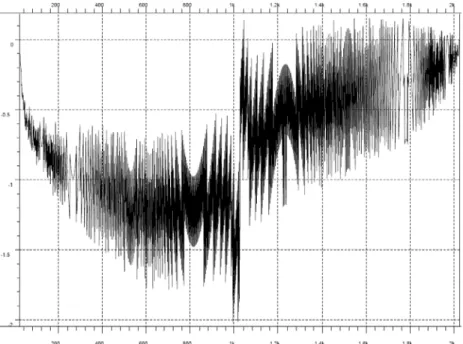
由圖可以知道,在低電阻時 OP 的 voltage noise 比電阻的 thermal noise 大,而且很接近電阻的 current noise,所以在電阻小於 1K 歐姆時不適合量測,在當電阻在 10K
Hsuan-Tien Lin (NTU CSIE) Machine Learning Foundations 5/25.. Noise and Error Noise and Probabilistic Target.
[r]
Wilson, Oriol Vinyals, “Learning the Speech Front-end With Raw Waveform CLDNNs,”.. In
