IEEE TRANSACTIONS ON MICROWAVE THEORY AND TECHNIQUES, VOL. 54, NO. 6, JUNE 2006 2321
Dual-Bandpass Filters With Serial Configuration
Using LTCC Technology
Ke-Chiang Lin, Chun-Fu Chang, Min-Chung Wu, and Shyh-Jong Chung, Senior Member, IEEE
Abstract—A dual-bandpass filter that utilizes a serial configu-ration of the inductive coupled-line (ICL) filter and the capacitive coupled-line (CCL) filter is investigated in this study. Numerical analysis is presented for the difference between the ICL and CCL filters. The dual-bandpass filter has a similar behavior to the indi-vidual single-band filter around the corresponding passband. An extra transmission zero can be generated between the two pass-bands of the dual-bandpass filter in that the ICL and CCL filters exhibit an out-of-phase response. Four architectures of dual-band-pass filters are proposed for the 2.4/5-GHz systems. Two of them are demonstrated by the low-temperature co-fired ceramic multi-layer technology. Measurements results agree quite well with the simulation ones.
Index Terms—Bandpass filter, dual-band, low-temperature co-fired ceramic (LTCC), wireless local area network (WLAN).
I. INTRODUCTION
W
ITH THE development of wireless local area networks (WLANs) rapidly growing, many products have been implemented in personal computers and peripheral to them, in addition to the mobile communication and consuming electronics. The IEEE 802.11 group established the WLAN standards including the 802.11 a/b/g. The 802.11 g uses the fre-quency from 2.4 to 2.4835 GHz and the orthogonal frefre-quency division multiplexing (OFDM) modulation with a data rate up to 54 Mb/s. The 802.11 a, covering the frequency range from 5.15 to 5.35 GHz (lower and middle U-NII bands) and from 5.725 to 5.825 GHz (upper U-NII band), utilizes the OFDM modulation with a data rate up to 54 Mb/s. Another standard, 802.11 j, adds channels in the frequency band of 4.9 to 5.0 GHz in Japan. Having 11–14 operation channels with 20-MHz bandwidth each, the 802.11 g only offers three nonoverlapped channels, whereas the 802.11 a provides more than ten nonoverlapped channels. To enhance the communication capacity of a unit cell, a dual-band system for the 802.11 a/g standard has been devel-oped to take advantage of these two specifications in the coming years. Fig. 1(a) shows a typical architecture of an RF dual-band front-end module. The module includes two diversity antennas, a double-pole-double-throw (DPDT) antenna and T/R switch, two diplexers, two low-pass filters, and two bandpass filters. InManuscript received September 26, 2005; revised February 24, 2006. This work was supported in part by the National Science Council, R.O.C., under Contract NSC 94-2752-E009-003-PAE and in part by the MOE ATU Program. K.-C. Lin, C.-F. Chang, and S.-J. Chung are with the Department of Commu-nication Engineering, National Chiao Tung University, Hsinchu, Taiwan 30050, R.O.C. (e-mail: [email protected]).
M.-C. Wu was with Department of Communication Engineering, National Chiao Tung University, Hsinchu, Taiwan 30050, R.O.C. He is now with the Yuen Foong Yu Group, Taipei, Taiwan, R.O.C.
Digital Object Identifier 10.1109/TMTT.2006.875267
front of the low-pass filters are the 2.4/5-GHz power amplifiers (PAs), and following the bandpass filters are the low-noise am-plifiers (LNAs). In this front-end module, there are six passive components used, which may occupy too much circuitry space. To reduce the size and also the cost of the module, the four single-band filters can be merged into two dual-band filters, as shown in Fig. 1(b). Each dual-band filter passes the signals of 2.4 and 5 GHz, and has a similar size to the single-band filters. Some dual-band components have been proposed such as a dual-band LNA [1], a dual-band RF front-end [2], and several dual-bandpass filters [3]–[8]. In [3], a dual-band-rejection filter was designed by using frequency-variable transformations. In [4], a dual-bandpass filter was implemented using three parallel open-ended stubs with one for a wide passband and the other two for the stopbands. A microstrip dual-bandpass filter [5] used stepped-impedance resonators (SIRs) in parallel-coupled and vertical-stacked configurations, and another dual-bandpass filter [6] utilized a wide bandpass filter in cascaded with a bandstop filter. Most of these designs need quite a bit of space to implement.
In this paper, motivated from the various designs of single-band filters [9]–[14], we introduce a new structure of single-bandpass filter, and, with its configuration, propose a new dual-bandpass filter. For size minimization, the filter is designed and demon-strated using low temperature co-fired ceramic (LTCC) multi-layer technology.
II. BANDPASS FILTER CONFIGURATION
WITHCAPACITIVECOUPLEDLINE(CCL)
A conventional bandpass filter with an inductive coupled line (ICL) is shown in Fig. 2(a). The filter has two capacitors, i.e., and , for dc blocking and impedance matching, as well as two resonators to form two poles in the passband. Each res-onator consists of a capacitor in parallel with a stripline . From the network analysis, the scattering param-eter of the filter can be expressed as [15]
(1)
where the constant is the characteristic impedance of the I/O ports, and , , , and , and the functions of are the transmission matrix elements. The frequency of the transmis-sion zero is determined by setting or, from (1), making , , , or approach infinity. For
sim-plifying the design, assume and .
2322 IEEE TRANSACTIONS ON MICROWAVE THEORY AND TECHNIQUES, VOL. 54, NO. 6, JUNE 2006
Fig. 1. (a) Conventional architecture of RF dual-band front-end module. (b) New architecture of RF dual-band front-end module with two dual-bandpass filters.
Fig. 2. (a) Conventional bandpass filter structure with an ICL. (b) New band-pass filter structure with a CCL.
By cascading the matrices, the transmission matrix ele-ments , , , and of the whole structure can be easily derived as
(2a)
(2b)
(2c)
where and . and
are the characteristic impedances of even and odd modes, respectively, and is the electrical length of the coupled line. The frequencies of the transmission zeros derived from
(2a)–(2c) by setting , , , and approach
infinity are
and (3)
where is the velocity of propagation in the coupled line, is the length of the coupled line, and is a nonnegative integer. This paper presents a new bandpass filter structure with a CCL, as shown in Fig. 2(b). The configuration is similar to the conventional ICL one, but with the orientation of one of the striplines opposed. The transmission matrix elements
LIN et al.: DUAL-BANDPASS FILTERS WITH SERIAL CONFIGURATION USING LTCC TECHNOLOGY 2323
Fig. 3. Magnitude responses of the transmission coefficient(S ) for the ICL and CCL filters designed at 2.4 GHz under the condition of equalizing all circuit parameters.
, , , and of this new structure are derived as
(4a)
(4b)
(4c)
and the corresponding frequencies of transmission zeros are
(5)
Comparing (5) and (3), the number of transmission zeros for the new CCL filter is half that of the ICL one. Fig. 3 shows the magnitude responses of transmission coefficient for the ICL and CCL filters designed at 2.4 GHz under the condition of equalizing all circuit parameters. It is seen that the two filters
Fig. 4. (a) Block diagram of the proposed dual-bandpass filter. (b) Circuit of the upper network (ICL filter) of the block diagram in (a). (c) Circuit of the lower network (CCL filter) of the block diagram in (a).
have the same performance at the lower frequency and the pass-band, but with differences at the higher frequency range caused by the transmission zeros. The additional zero for the conven-tional ICL filter at the frequency of sharpens the high skirt of the passband. Besides, due to the reverse connection at the output port, the ICL and CCL filters exhibit an out-of-phase re-sponse at the frequency range before the first zero. This prop-erty benefits the design of the dual-bandpass filters, as will be demonstrated below.
III. NEWDUAL-BANDPASSFILTERCONFIGURATIONS
A. Circuit Model
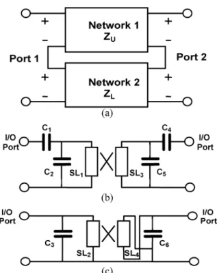
The structure of the proposed dual-bandpass filter consists of the ICL and CCL filters with a serial configuration. Fig. 4(a) shows the block diagram of the dual-bandpass filter where the upper network (Network 1) is responsible for the low passband and the lower network (Network 2) is responsible for the high passband. The circuits of the upper and lower networks are de-picted, as examples, in Fig. 4(b) and (c). Here, the dual-bandpass filter with the ICL configuration at low band (2.4 GHz) and the CCL at high band (5 GHz) is illustrated. The dc block capacitors of the lower network in Fig. 4(c) are left out for simplification. With a serial configuration, the total impedance could be written as
(6)
where is the dual-bandpass filter impedance matrix and and are the impedance matrices of the upper [see Fig. 4(b)]
2324 IEEE TRANSACTIONS ON MICROWAVE THEORY AND TECHNIQUES, VOL. 54, NO. 6, JUNE 2006
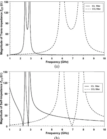
Fig. 5. Magnitude responses of: (a) the trans-impedanceZ and (b) the self-impedanceZ for the ICL and CCL filters in Fig. 4.
and lower [see Fig. 4(c)] networks, respectively. Fig. 5(a) and (b) shows the magnitudes, as functions of frequency, of the trans-impedance and self-impedance , respectively, for the individual single-band filters.
The low-band filter (ICL filter) possesses two resonance poles at 2.3 and 2.7 GHz, while the high-band filter (CCL filter) has poles at 5.7 and 7.7 GHz. Note that the magnitudes of the im-pedances ( and ) of the high-band filter are neg-ligible around the low passband, as compared to those ( and ) of the low-band filter, and vice versa. This implies that the series-connected dual-bandpass filter has about the same impedance values as the low-band filter around the low pass-band and as the high-pass-band filter near the high passpass-band. Thus, by the conversion of the transmission coefficient expressed as a function of the corresponding impedance matrix elements as [15]
(7)
the transmission coefficient of the dual-bandpass filter has ap-proximately the same behavior as the individual single-band filter around the corresponding passband. It should be noticed from Fig. 5(b) that the low-band filter has a stronger loading effect on the high-band one so that, as can be seen later, the
Fig. 6. Four architectures of the proposed dual-bandpass filter with: (a) ICL for low band and CCL for high band (2I5C), (b) CCL for low band and ICL for high band (2C5I), (c) ICL for both bands (2I5I), and (d) CCL for both bands (2C5C).
TABLE I
COUPLED-LINETYPES INNETWORKS1AND2,AND THECORRESPONDING
DESIGNPARAMETERS FOR THEDUAL-BANDPASSFILTERS
(The unit for capacitors is pF and that for transmission line is mm.)
two high-band poles will be shifted a little toward the lower fre-quencies (5.2 and 5.8 GHz) when the two single-band filters are stacked up.
The frequencies of transmission zeros are determined by set-ting or, from (7), . As the ICL and CCL fil-ters perform opposite phase characteristics, the trans-impedance
can generate zero with and canceling each other at the frequency of equal magnitudes. From Fig. 5(a), the magnitudes are equal at the frequencies near 3.4 and 1 GHz. This means that the total trans-impedance of the dual-bandpass filter would sum to zero, thus producing trans-mission zeros at these frequencies.
In this paper, four architectures, as shown in Fig. 6, of the pro-posed dual-bandpass filter are designed and compared. Fig. 6(a) comprises the ICL filter at the low band and the CCL filter at the high band (called “2I5C” in this paper) and Fig. 6(b) conversely sets CCL filter at the low band and the ICL filter at the high band (2C5I). Fig. 6(c) utilizes two ICL filters in low and high
LIN et al.: DUAL-BANDPASS FILTERS WITH SERIAL CONFIGURATION USING LTCC TECHNOLOGY 2325
TABLE II
PHYSICALLAYOUTPARAMETERSACCORDING TOFIG. 7 (2I5C)
bands (2I5I) and Fig. 6(d) uses two CCL filters in both two bands (2C5C). Table I summarizes the coupled-line types in Network 1 and Network 2 and also shows the design parameters for the four filters.
B. Transformation of Circuit Model to Physical Layout
The proposed filter architectures are composed of capaci-tors and coupled transmission lines. To implement a capacitor in the LTCC substrate, the parallel-plate capacitance formula is used, where is the dielectric constant of the ceramic material, is the overlap area between the two parallel plates, and is the distance between the two parallel plates. For considering the fabrication tolerance, one of the two plates is designed larger than it is supposed to be so that the capacitance would not vary much while one of these plates is shifted due to process inaccuracy. Actually the obtained sizes of the plates need to be fine tuned in the electromagnetic (EM) simulation by taking the cause of the fringing field into account. After the ca-pacitors are done, we then design the transmission lines based on the parameters from the circuit simulation. Notably, the mutual coupling of the metal plates in this compact multilayer struc-ture would result in different simulation responses from the cir-cuit simulator so we have to adjust them to reduce the parasitic effects as best we can in order to minimize the difference be-tween the full-wave simulation and circuit simulation. Due to the process limit, the minimum linewidth, minimum spacing between lines, and minimum via diameter are 0.1, 0.075, and 0.1 mm, respectively. By the restriction of the spacing between lines, the coupling is not strong enough to make a wide pass-band at 5 GHz, even though the minimum spacing has been ap-plied. Therefore, the broadside coupled line is utilized at 5 GHz to derive enough coupling. The edge coupled line at 2 GHz supports satisfactory bandwidth with the minimum line spacing of 0.075 mm. Table II depicts the LTCC layout parameters ac-cording to Fig. 7.
C. LTCC Layout and EM Simulation
The four dual-bandpass filters have the same size of 2.5 mm 2.0 mm 0.94 mm and are all designed using the 16 LTCC layers. The thickness of each layer is 0.035 mm, except Layer 3, which is 0.07 mm. The material of the LTCC used here is CT2000, which has a dielectric constant of 9.1, loss tangent of 0.002, and metal thickness of 0.012 mm. As an example, Fig. 7
Fig. 7. Layout of the 2I5C dual-bandpass filter with size of 2.5 mm22.0 mm2 0.94 mm.
illustrates the layout of the 2I5C dual-bandpass filter. The LTCC has three ground layers on Layer 1, Layer 3, and Layer 16, and the locations and metal sizes of other elements are marked as shown in Fig. 7. For convenience, the elements are laid out sym-metrically, except the CCL of 5 GHz. Port 1 and Port 2 are on Layer 11 and the dc block capacitors ( and ) are produced by the metals on Layer 10 and Layer 11, respectively. Since the resonator capacitors ( and ) of 2.4 GHz are too large to be made by two layers, we use several parallel metals to form the capacitors from Layers 7 to 10. The metals on Layers 7 and 9 have equal potential by a via (which is electrically connected with electric circuit layers), as do the metals on Layer 8 and Layer 10. The other resonator capacitors ( and ) of 5 GHz are made by the metals on Layer 7 and ground Layers 1 and 3. Ground Layer 3 is used to provide sufficient capacitance for and because the distance between Layer 1 and Layer 7 is too large. The ICL of 2.4 GHz on layer 9 uses the edge coupling and the CCL of 5 GHz on Layers 2 and 3 uses the broadside cou-pling that can provide much coucou-pling to produce a wide pass-band. Ground Layer 1 is slotted to decrease the parasitic effect between Layer 1 and the CCL on Layer 2. Similarly, the bottom ground Layer 16 is designed to avoid the undesired capacitors associated with the metal on Layer 11.
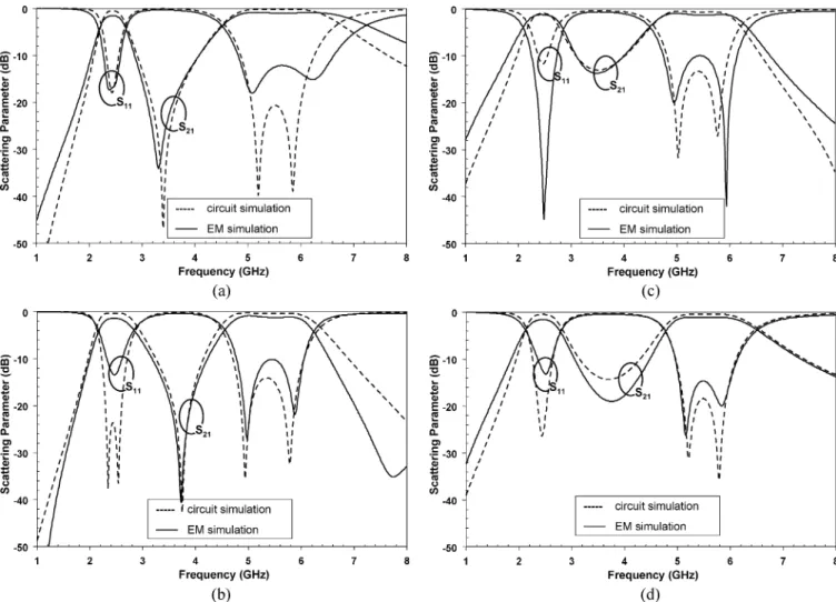
The ideal circuit simulations by the circuit simulator Mi-crowave Office [16] and EM simulations by the full-wave commercial package HFSS [17] are presented in Fig. 8 for the four dual-bandpass filters. The dashed lines are the results from the ideal circuit simulation and the solid lines are from the EM simulation. The simulation response of Fig. 8(a) [see Fig. 8(b)] that uses the ICL (CCL) filter at 2.4 GHz and the CCL (ICL) filter at 5 GHz has the insertion loss of 1.6 dB ( 1.4 dB) at a low passband and 1.0 dB ( 1.2 dB) at a high passband. The two poles of the high passband are designed at approximately 5 and 6 GHz to form a wide bandwidth in Fig. 8(a) and (b).
2326 IEEE TRANSACTIONS ON MICROWAVE THEORY AND TECHNIQUES, VOL. 54, NO. 6, JUNE 2006
Fig. 8. Circuit simulation and EM simulation of the dual-bandpass filters. (a) 2I5C. (b) 2C5I. (c) 2I5I. (d) 2C5C.
Expectantly due to the opposite phase, there is a transmission zero near 3.5 GHz between the two passbands. (The zero has a benefit rejection of Worldwide Interoperability for Microwave Access (WiMAX) signals to increase isolation.) Since the magnitude response of the ICL filter decays quicker than that of the CCL filter in higher frequency, the performance of Fig. 8(b) has the sharper response in the high band than Fig. 8(a). In Fig. 8(c) [see Fig. 8(d)] that uses the ICL (CCL) filter at both 2.4 and 5 GHz, the insertion losses are 1.2 dB ( 1.5 dB) at 2.4 GHz and 1.0 dB ( 1.2 dB) at 5 GHz. Since the filters in Fig. 8(c) and (d) use the same types of coupled line, no obvious transmission zeros occur in between the two passbands. With the reason of quicker decaying stated above, Fig. 8(c) has a better rejection at the high frequency than Fig. 8(d).
IV. MEASUREMENTRESULTS
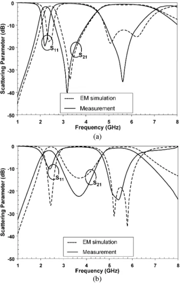
Two dual-bandpass filters, i.e., 2I5C and 2C5C, were fabri-cated using the LTCC technology for demonstration. The EM simulation (dashed line) and measurement (solid line) of these two dual-bandpass filters are presented in Fig. 9(a) and (b). For the results of the 2I5C filter shown in Fig. 9(a), the measured transmission coefficient agrees quite well with the simu-lated one in the high passband, but with a little frequency shift (approximately 200 MHz) in the low passband. The filter has a
measured insertion loss of approximately 1.8 dB at 2.2 GHz and approximately 1.0 dB from 4.9 to 5.9 GHz. The trans-mission zero is located at 3.17 GHz with the suppression under 40 dB. The frequency shift in the low band is caused by the fact that the shrinkage of layer thickness with circuit printing is larger than that without printing, i.e., printed Layers 7–11 of the 2I5C layout in Fig. 7 shrink more than unprinted Layers 4–6. Thus, the capacitors of 2.4-GHz circuitry laid on Layers 7–11 become larger than the designed ones, leading to the down shift of the low passband. Contrarily, the 5-GHz high band is laid on Layers 1–7 so the thickness is similar to the design, and the mea-sured result of fits the EM simulation. However, in the high passband, while we lay out the CCL with broadside coupling, a little offset between layers weakens the coupling such as to reshape two poles into a sharp one, as observed in this figure.
The measured results of dual-bandpass filter 2C5C are illus-trated in Fig. 9(b). The insertion loss is 2.1 dB at 2.3 GHz and is 1.3 dB from 5.0 to 5.6 GHz. Without the obvious transmis-sion zeros between two passbands, the 2C5C filter still has the suppression more than 20 dB at 3.6 GHz. Due to the same factor of 2I5C, the 2.4-GHz passband also shifts to a lower fre-quency by approximately 100 MHz. Owing to the offset of the CCL with broadside coupling in the high passband, the band-width is reduced. Fig. 10 shows the photograph of these two LTCC dual-bandpass filters.
LIN et al.: DUAL-BANDPASS FILTERS WITH SERIAL CONFIGURATION USING LTCC TECHNOLOGY 2327
Fig. 9. Simulation and measurement results of: (a) the 2I5C dual-bandpass filter and (b) the 2C5C dual-bandpass filter.
Fig. 10. Two dual-bandpass LTCC filters.
V. CONCLUSION
In this study, a CCL bandpass filter is analyzed and com-pared with the ICL bandpass filter. Applying the CCL, the filter design becomes more flexible over the conventional ICL de-signs. By stacking up the ICL and CCL filters, we introduce a new structure of the dual-bandpass filter that has a low in-sertion loss in both passbands and a wide bandwidth in the high band. With a serial configuration of the ICL and CCL fil-ters, a transmission zero could be generated between two pass-bands. Two dual-bandpass filters are fabricated in a compact size using the LTCC process. Satisfying performances are achieved
in both circuit and EM simulations. The transmission zero of the dual-bandpass filter at near 3.5 GHz has a profit rejection of WiMAX signals. Based on the proposed stack-up dual-bandpass configuration for WLAN applications, filters with more trans-mission zeros at frequencies such as those of the mobile com-munication systems (0.9/1.8/1.9 GHz) are to be developed in the near future.
ACKNOWLEDGMENT
The authors are grateful to the Mag.Layers Scientific-Tech-nics Company Ltd., Hsin-Chu, Taiwan, R.O.C., for LTCC fabrication. Much appreciation is expressed to C.-Y. Wei, Mag.Layers Scientific-Technics Company Ltd., for helpful dis-cussions. The reviewers are also appreciated for their valuable comments and suggestions.
The proposed filter schematic presented in this paper is patent pending.
REFERENCES
[1] H. Hashemi and A. Hajimiri, “Concurrent multiband low-noise ampli-fiers—Theory, design, and applications,” IEEE Trans. Microw. Theory
Tech., vol. 50, no. 1, pp. 288–301, Jan. 2002.
[2] J. Ryynänen, K. Kivekäs, J. Jussila, A. Pärssinen, and K. A. I. Halonen, “A dual-band RF front-end for WCDMA and GSM applications,” IEEE
J. Solid-State Circuits, vol. 36, no. 8, pp. 1198–1204, Aug. 2001.
[3] H. Uchida, H. Kamino, K. Totani, N. Yoneda, M. Miyazaki, Y. Konishi, S. Makino, J. Hirokawa, and M. Ando, “Dual-band-rejection filter for distortion reduction in RF transmitters,” IEEE Trans. Microw. Theory
Tech., vol. 52, no. 11, pp. 2550–2556, Nov. 2004.
[4] V. Palazzari, S. Pinel, J. Laskar, L. Roselli, and M. M. Tentzeris, “Design of an asymmetrical dual-band WLAN filter in liquid crystal polymer (LCP) system-on-package technology,” IEEE Micro. Wireless
Compon. Lett., vol. 15, pp. 165–167, Mar. 2005.
[5] J.-T. Kuo, T.-H. Yeh, and C.-C. Yeh, “Design of microstrip bandpass filters with a dual-passband response,” IEEE Trans. Microw. Theory
Tech., vol. 53, no. 4, pp. 1331–1337, Apr. 2005.
[6] L.-C. Tsai and C.-W. Hsue, “Dual-band bandpass filters using equal-length coupled-serial-shunted lines andz-transform technique,” IEEE
Trans. Microw. Theory Tech., vol. 52, no. 4, pp. 1111–1117, Apr. 2004.
[7] C.-H. Chang, H.-S. Wu, H. J. Yang, and C.-K. C. Tzuang, “Coalesced single-input single-output dual-band filter,” in IEEE MTT-S Int.
Mi-crow. Symp. Dig., Jun. 2003, vol. 1, pp. 511–514.
[8] H. Miyake, S. Kitazawa, T. Ishizaki, T. Yamada, and Y. Nagatomi, “A miniaturized monolithic dual band filter using ceramic lamination tech-nique for dual mode portable telephones,” in IEEE MTT-S Int. Microw.
Symp. Dig., 1997, pp. 789–792.
[9] A. Podcameni, “Symmetrical and asymmetrical edge-coupled-line impedance transformers with a prescribed insertion loss design,” IEEE
Trans. Microw. Theory Tech., vol. MTT-34, no. 1, pp. 1–7, Jan. 1986.
[10] L. K. Yeung and K.-L. Wu, “A compact second-order LTCC bandpass filter with two finite transmission zeros,” IEEE Trans. Microw. Theory
Tech., vol. 51, no. 2, pp. 337–341, Feb. 2003.
[11] C.-W. Tang, Y.-C. Lin, and C.-Y. Chang, “Realization of transmis-sion zeros in combline filters using an auxiliary inductively coupled ground plane,” IEEE Trans. Microw. Theory Tech., vol. 51, no. 10, pp. 2112–2118, Oct. 2003.
[12] K. Rambabu and J. Bornemann, “Simplified analysis technique for the initial design of LTCC filters with all-capacitive coupling,” IEEE Trans.
Microw. Theory Tech., vol. 53, no. 5, pp. 1787–1791, May 2005.
[13] C.-F. Chang and S.-J. Chung, “Bandpass filter of serial configuration with two finite transmission zeros using LTCC technology,” IEEE
Trans. Microw. Theory Tech., vol. 53, no. 7, pp. 2383–2388, Jul. 2005.
[14] C.-H. Lee, S. Chakraborty, A. Sutono, S. Yoo, D. Heo, and J. Laskar, “Broadband highly integrated LTCC front-end module for IEEE 802.11a WLAN applications,” in IEEE MTT-S Int. Microw. Symp.
Dig., Jun. 2002, vol. 2, pp. 1045–1048.
[15] D. M. Pozar, Microwave Engineering, 2nd ed. New York: Wiley, 1998.
[16] Microwave Office. Appl. Wave Res. Inc., El Segundo, CA, 2002. [17] HFSS. Ansoft Corporation, Pittsburgh, PA, 2001.
2328 IEEE TRANSACTIONS ON MICROWAVE THEORY AND TECHNIQUES, VOL. 54, NO. 6, JUNE 2006
Ke-Chiang Lin was born in Taoyuan, Taiwan, R.O.C., on November 12, 1981. He received the B.S. degree in electrical engineering from National Sun Yat-Sen University (NSYSU), Kaohsiung, Taiwan, R.O.C., in 2004, and is currently working toward the M.S. degree in communication engineering at National Chiao Tung University (NCTU), Hsinchu, Taiwan, R.O.C.
His research interests are LTCC RF passive com-ponents and microwave circuits.
Chun-Fu Chang was born in Kaohsiung, Taiwan, R.O.C., on February 1, 1982. He received the B.S. degree in communication engineering from National Chiao Tung University, Hsinchu, Taiwan, R.O.C., in 2004, and is currently working toward the M.S. de-gree in communication engineering at National Chiao Tung University.
His currently research interests are microwave circuits, LTCC RF passive components, and LTCC front-end modules for WLAN applications.
Min-Chung Wu was born in Taoyuan, Taiwan, R.O.C., on February 15, 1980. He received the M.S. degree in communication engineering from National Chiao Tung University (NCTU), Hsinchu, Taiwan, R.O.C., in 2005.
He is currently with the Yuen Foong Yu Group, Taipei, Taiwan, R.O.C.
Shyh-Jong Chung (M’92–SM’06) was born in Taipei, Taiwan, R.O.C. He received the B.S.E.E. and Ph.D. degrees from National Taiwan University, Taipei, Taiwan, R.O.C., in 1984 and 1988, respec-tively.
Since 1988, he has been with the Department of Communication Engineering, National Chiao Tung University, Hsinchu, Taiwan, R.O.C., where he is cur-rently a Professor. From September 1995 to August 1996, he was a Visiting Scholar with the Department of Electrical Engineering, Texas, A&M University, College Station. He was the leader of a sub-program in the four-year Advanced Technologies for Telecommunications National Research Program, which was supported by the Ministry of Education, Taiwan, R.O.C. He has authored or coauthored over 70 technical papers in international journals or conferences in-cluding several invited papers and speeches. His areas of interest include the design and applications of active and passive planar antennas, communications in intelligent transportation systems (ITSs), LTCC-based RF components and modules, packaging effects of microwave circuits, and numerical techniques in electromagnetics.