Enhanced conversion efficiency of a crystalline
silicon solar cell with frustum nanorod arrays
Min-An Tsai,2 Ping-Chen Tseng,1 Hsin-Chu Chen,1 Hao-Chung Kuo,1 and Peichen Yu,1* 1 Department of Photonics and Institute of Electro-Optical Engineering, National Chiao Tung University, Hsinchu
30010, Taiwan, China
2 Department of Electro-physics, National Chiao Tung University, Hsinchu 30010, Taiwan, China * [email protected]
Abstract: Enhanced photoelectric conversion is demonstrated in a crystalline silicon (c-Si) solar cell with frustum nanorod arrays (FNAs), fabricated using colloidal lithography and reactive-ion etching techniques. Under a simulated one-sun condition, the cell with FNAs improves the power conversion efficiency by nearly 30%, compared to a conventional wet-chemical-textured reference. The enhancement mostly arises from the superior antireflective properties for wavelengths between 400 nm and 1000 nm. In that spectral range, we show that photons gained by reflection reduction directly contribute to collected carriers without auxiliary losses due to nano-fabrication. Moreover, the omnidirectional antireflection of FNAs is also investigated using an angle-resolved reflectance spectroscopy. The dimensions of FNAs are further analyzed with numerical calculations based on Maxwell’s equations. The optimized short-circuit current density achieves nearly 40 mA/cm2, corresponding to a 16% enhancement compared to the conventional device.
©2010 Optical Society of America
OCIS codes: (310.6628) Subwavelength structures, nanostructures; (040.5350) Photovoltaic.
References and links
1. C. Lee, S. Y. Bae, S. Mobasser, and H. Manohara, “A novel silicon nanotips antireflection surface for the micro Sun sensor,” Nano Lett. 5(12), 2438–2442 (2005).
2. Y. J. Lee, D. S. Ruby, D. W. Peters, B. B. McKenzie, and J. W. P. Hsu, “ZnO nanostructures as efficient antireflection layers in solar cells,” Nano Lett. 8(5), 1501–1505 (2008).
3. M. A. Tsai, P. Yu, C. L. Chao, C. H. Chiu, H. C. Kuo, S. H. Lin, J. J. Huang, T. C. Lu, and S. C. Wang, “Efficiency enhancement and beam shaping of GaN–InGaN vertical-injection light-emitting diodes via high-aspect-ratio nanorod arrays,” IEEE Photon. Technol. Lett. 21(4), 257–259 (2009).
4. Y. A. Chang, Z. Y. Li, H. C. Kuo, T. C. Lu, S. F. Yang, L. W. Lai, L. H. Lai, and S. C. Wang, “Efficiency improvement of single-junction InGaP solar cells fabricated by a novel micro-hole array surface texture process,” Semicond. Sci. Technol. 24(8), 085007 (2009).
5. D. J. Aiken, “High performance anti-reflection coatings for broadband multi-junction solar cells,” Sol. Energy Mater. Sol. Cells 64(4), 393–404 (2000).
6. W. H. Southwell, “Gradient-index antireflection coatings,” Opt. Lett. 8(11), 584–586 (1983).
7. J. A. Dobrowolski, D. Poitras, P. Ma, H. Vakil, and M. Acree, “Toward perfect antireflection coatings: numerical investigation,” Appl. Opt. 41(16), 3075–3083 (2002).
8. D. Poitras, and J. A. Dobrowolski, “Toward perfect antireflection coatings. 2. Theory,” Appl. Opt. 43(6), 1286– 1295 (2004).
9. E. Oliva, F. Dimroth, and A. W. Bett, “GaAs converters for high power densities of laser illumination,” Prog. Photovol. 16(4), 289–295 (2008).
10. M. E. Motamedi, W. H. Southwell, and W. J. Gunning, “Antireflection surfaces in silicon using binary optics technology,” Appl. Opt. 31(22), 4371–4376 (1992).
11. P. Lalanne, and G. M. Morris, “Antireection behavior of silicon subwavelength periodic structures for visible light,” Nanotechnology 8(2), 53–56 (1997).
12. Y. Kanamori, K. Hane, H. Sai, and H. Yugami, “100 nm period silicon antireflective structures fabricated using a porous alumina membrane mask,” Appl. Phys. Lett. 78(2), 142–143 (2001).
13. Y. F. Huang, S. Chattopadhyay, Y. J. Jen, C. Y. Peng, T. A. Liu, Y. K. Hsu, C. L. Pan, H. C. Lo, C. H. Hsu, Y. H. Chang, C. S. Lee, K. H. Chen, and L. C. Chen, “Improved broadband and quasi-omnidirectional anti-reflection properties with biomimetic silicon nanostructures,” Nat. Nanotechnol. 2(12), 770–774 (2007). 14. C. H. Chiu, P. Yu, H. C. Kuo, C. C. Chen, T. C. Lu, S. C. Wang, S. H. Hsu, Y. J. Cheng, and Y. C. Chang,
8748–8754 (2008).
15. C. H. Chang, P. Yu, and C. S. Yang, “Broadband and omnidirectional antireflection from conductive indium-tin-oxide nanocolumns prepared by glancing-angle deposition with nitrogen,” Appl. Phys. Lett. 94(5), 051114 (2009).
16. P. Yu, C. H. Chang, C. H. Chiu, C. S. Yang, J. C. Yu, H. C. Kuo, S. H. Hsu, and Y. C. Chang, “Efficiency enhancement of GaAs photovoltaics employing anti-reflective indium-tin-oxide nano-columns,” Adv. Mater.
21(16), 1–4 (2009).
17. G. R. Lin, Y. C. Chang, E. S. Liu, H. C. Kuo, and H. S. Lin, “Low refractive index Si nanopillars on Si substrate,” Appl. Phys. Lett. 90(18), 181923 (2007).
18. C. H. Sun, W. L. Min, N. C. Linn, P. Jiang, and B. Jiang, “Templated fabrication of large area subwavelength antireflection gratings on silicon,” Appl. Phys. Lett. 91(23), 231105 (2007).
19. C. C. Striemer, and P. M. Fauchet, “Dynamic etching of silicon for broadband antireflection applications,” Appl. Phys. Lett. 81(16), 2980–2982 (2002).
20. T. Lohmüller, M. Helgert, M. Sundermann, R. Brunner, and J. P. Spatz, “Biomimetic interfaces for high-performance optics in the deep-UV light range,” Nano Lett. 8(5), 1429–1433 (2008).
21. Y. Kanamori, M. Sasaki, and K. Hane, “Broadband antireflection gratings fabricated upon silicon substrates,” Opt. Lett. 24(20), 1422–1424 (1999).
22. M. A. Tsai, P. Yu, C. H. Chiu, H. C. Kuo, T. C. Lu, and S. H. Lin, “Self-Assembled two-dimensional surface structures for beam shaping of GaN-based vertical-injection light-emitting diodes,” IEEE Photon. Technol. Lett.
22(1), 12–14 (2010).
23. H. Sai, H. Fujii, K. Arafune, Y. Ohshita, M. Yamaguchi, Y. Kanamori, and H. Yugami, “Antireective subwavelength structures on crystalline Si fabricated using directly formed anodic porous alumina masks,” Appl. Phys. Lett. 88(20), 201116 (2006).
24. P. C. Tseng, H. C. Chen, and M. A. Tsai, H. C. K, and P. Yu,” Angle-resolved characteristics of silicon photovoltaics with passivated conical-frustum nanostructures,” unpublished.
1. Introduction
Fresnel reflection of incident light arises from the large refractive index discontinuity at the interface of two medium, especially for air and semiconductor materials. The high reflective index of Si results in optical reflection loss up to 37% for the incident light, which severely limits the performance of Si-based optoelectronic devices, particularly for solar cells, displays, and light sensors [1,2]. For Si-based solar cells, a key method to increase the external quantum efficiency (EQE) is to reduce interfacial Fresnel reflection in the absorption regime of silicon [3,4]. Therefore, effective antireflective coatings (ARCs) are particularly important. The conventional multilayer ARCs are usually composed of a quarter wavelength stack of dielectrics with different refractive indices, such as silicon nitride or silicon dioxide [5–8]. However, these multilayer ARCs are expensive to fabricate owing to stringent requirements in the high-vacuum deposition, material selection, and layer thickness control, etc.. Additionally, thermal-mismatch-induced lamination and material diffusion of the multilayer ARCs can further limit the device performance at high power densities [9].
Since the corneas of nocturnal-moth eyes were found to have broadband antireflective properties, surface-relief arrays with dimensions smaller than the wavelength of incident light have been considered an alternative to thin-film coatings. The sub-wavelength structures are also more stable and durable than surface coatings since only one material is involved. Over the past decade, increasing efforts onto the fabrication of such surface antireflective structures has been devoted [10–16]. Many different structures, such as nano-cones or nano-pyramids [17–20], have been created in order to suppress the surface reflection. The basic purpose of this technique is to introduce a gradient refractive index layer between air and the substrate material by the spatial profile of nanostructures. As a result, reflection can be substantially suppressed for a wide spectral bandwidth and over a large angle of incidence (AOI) [21]. However, most of the nanostructures suggest a tapered profile with sharp tips which may not be preferred in solar cells due to considerable surface states that trap photo-generated carriers. The sharp tips also increase the challenge in making ohmic contacts for electrodes. Therefore the design of nanostructures with a gradient refractive-index property for antireflection and a flat surface for ohmic contacts becomes the key elements to achieve high-efficiency solar cells. In this paper, we demonstrate the implementation of frustum nanorod arrays (FNA) in c-Si solar cells. The FNAs are fabricated on a p-type crystalline silicon (c-c-Si) substrate utilizing polystyrene colloidal lithography and reactive-ion etching (RIE) techniques [22].
We show that the cell with FNAs improves the power conversion efficiency by nearly 30%, compared to a conventional wet-chemical-textured reference. The enhancement mostly arises from the broadband and omnidirectional antireflective properties, confirmed by the quantum efficiency analysis and an angle-resolved reflectance spectroscopy. Moreover, the diameter and the height of the FNAs are also optimized using numerical simulations based on Maxwell’s equations.
2. Fabrication
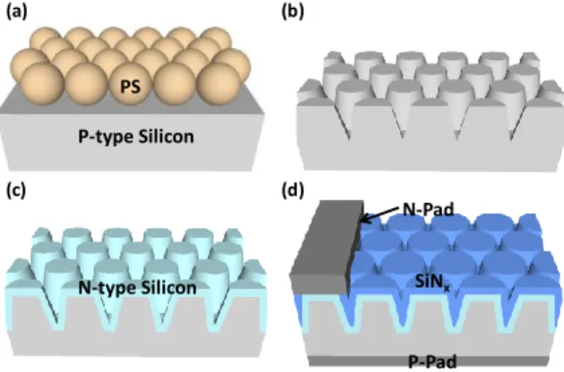
The fabrication of c-Si solar cells with FNAs began with the use of colloidal lithography. As schematically illustrated in Fig. 1(a), a monolayer of self-assembled polystyrene (PS) nanospheres with a plurality of 10 wt% was spin-cast onto the surface of a p-type c-Si substrate. By turning the degree of hydrophilicity, spinning speed, and the mixture concentration, a nearly-close-packed PS nanospheres monolayer was obtained on the c-Si substrate. Here, we chose PS nanospheres with a diameter of 600 nm as shadow masks. After steady air-drying for 15 minute, the sample shown in Fig. 1(a) were etched by an inductively coupled plasma reactive ion etching (ICP-RIE) system, where a reactive gas Cl2 was introduced to bombard the nanospheres and the underlying c-Si substrate simultaneously with an RF power of 1000 W, a bias power of 150 W, under a 5 mTorr pressure at 60°C for 70 seconds. The etching selectivity of PS and c-Si was approximately 1:3.5. Thereafter, the sample was brushed and dipped into a pure acetone solution for 5 minutes at room temperature, which resulted in nearly close-packed FNAs on the c-Si surface, as shown in Fig. 1(b). Next, the textured substrate was doped using phosphorus oxychloride (POCl3) as the diffusion source to form an n-type layer, ~200 nm deep from the surface. After the removal of the phosphosilicate glass (PSG) layer from the substrate surface with diluted hydrofluoric (HF) acid, as shown in Fig. 1(c), an 80-nm-thick silicon nitride (SiNx) layer was deposited to passivate the surface by using plasma-enhanced chemical vapor deposition (PECVD). The PSG removal also mitigates the surface damages of FNAs due to RIE. Finally the front and back metal contacts were screen-printed and a co-firing in a furnace system at 850°C, as shown in Fig. 1(d). For comparison, a conventional c-Si solar cell was also fabricated simultaneously after the formation of surface textures as the reference. The KOH-etched pyramidal surface textures exhibit ~few micrometers in height and in base widths, which are quite standard in commercial mono-crystalline solar cells.
P-type Silicon PS
N-type Silicon SiNx
N-Pad
P-Pad
(a) (b)
(c) (d)
Fig. 1. The schematic fabrication flow for a silicon solar cell with frustum nanorod arrays (FNAs): (a) spin-cast of nearly-close-packed polystyrene nanospheres monolayer, (b) resulting FNAs after dry etching, (c) diffusion of an N-type layer. (d) SiNx deposition and screen
printing of the front and back electrodes.
As seen in Fig. 2(a), the scanning electron microscopic (SEM) images of the resulting c-Si FNAs show that the periodicity is accurately transferred onto the Si substrate after RIE. The height and shape of FNA can be controlled by varying the etching duration and conditions. As
shown in Fig. 2(b), the height of the FNAs is ~350 nm, while the top and bottom diameter are ~400 nm and 600 nm, respectively.
1um 300 nm
(a) (b)
Fig. 2. Scanning electron microscopic (SEM) images of the fabricated frustum nanorod arrays: (a) a 45-degree tilted top view, (b) a cross-sectional view.
3. Measurement and analysis
Figure 3(a) shows the total reflectance spectra of c-Si solar cell with FNAs and with a conventional potassium hydroxide (KOH)-etched surface textures measured using an integrating sphere at the normal incidence of light. An arbitrary-unit AM1.5G solar cell spectrum is also plotted for reference. The solar cell with FNAs reveals superior antireflective properties for the silicon absorption range, especially in the short wavelength (<550nm) and long wavelength (>700nm) regions, compared to the KOH-textured cell. For short-wavelength photons, the structural profile of FNAs gives rise to a gradient refractive index profile, which reduces the Fresnel reflection. For long-wavelength photons, the FNAs behave as a porous layer of which the effective refractive index buffers the index discontinuity between air and silicon [23]. The external quantum efficiency (EQE), defined as the number of elementary charges collected at the contacts divided by the number of photons impinging on the device, is also characterized for both devices, as shown in Fig. 3(b). The suppression of the Fresnel reflection contributes to enhanced optical absorption, which is also reflected in the EQE characteristics. However, in order to investigate auxiliary losses potentially due to the nano-faction, the photons gained by reflection reduction needs to be balanced against the collected carriers. Figure 3(c) presents the calculated improvement factors of optical absorption, ΔA and the EQE, ΔEQE, which are defined as ΔA = (1-RFNA)/(1-RKOH) and ΔEQE = EQEFNA/EQEKOH, respectively. As seen in Fig. 3(c), both curves agree with each other very well, suggesting negligible loss mechanisms resulting from the fabrication of FNAs. The ΔEQE near 400 nm and 1000 nm wavelengths improves even further than ΔΑ, indicating an improved front and back surface recombination, which may explain the slight difference in the open-circuit voltages and fill factors for both devices.
(a) (b) (c) 400 500 600 700 800 900 1000 0 10 20 30 40 50 60 Reflection (%) Wavelength (nm) KOH wet-etching LSNA AM 1.5G 400 500 600 700 800 900 1000 1100 0 20 40 60 80 100 EQE (%) Wavelength (nm) Reference FNAs R ef le ct an ce ( % ) 400 500 600 700 800 900 1000 1100 0 20 40 60 80 100 EQE (%) Wavelength (nm) Reference FNAs 400 500 600 700 800 900 1000 0.9 1.0 1.1 1.2 1.3 Im p ro v e m e n t fa c to r Wavelength (nm) 400 500 600 700 800 900 1000 1100 0 20 40 60 80 100 EQE (%) Wavelength (nm) Reference
FNAsAbsorptionEQE
Imp ro ve me n t fa ct or
Fig. 3. (a) The measured reflectance spectra for cells with frustum nanorod arrays (FNAs) and KOH-etched textures (the reference). The AM1.5G spectrum is also plotted in arbitrary unit. (b) The corresponding external quantum efficiency (EQE) characteristics; (c) the improvement factors for optical absorption (ΔA) and EQE (ΔEQE).
The current-voltage (I–V) characteristics were measured under a simulated AM1.5G illumination condition at room temperature, and summarized in Table Ι for solar cells with FNAs and conventional micro-textures. The short-circuit current density (Jsc) of the cell with FNAs achieves 37.59 mA/cm2, while the power conversion efficiency is increased from 12.01% to 15.43%, corresponding to a 28.48% enhancement compared to that of the reference. The open-circuit voltage (Voc) and fill-factor (FF) are also slightly improved, which most likely arise from the non-uniformity during contact formation. It requires further investigation to resolve whether such improvements are due to process variations or actually result from fine metal contacts due to different surface areas between FNAs and micro-textures.
Table 1. Current-Voltage Characteristics of c-Si Solar Cells with Various Surface Structures. Type Voc (V) Jsc (mA/cm2) FF (%) η (%) Rs (mΩ) Rsh (Ω) *FNAs 0.60 37.59 68.41 15.43 25.2 819 Micro-textures 0.59 34.22 59.49 12.01 45.4 176 * FNAs: frustum nanorod arrays
4. Angular reflectivity
The incident-angle-dependent reflection properties are important to solar cells due to the sun movement. Here, we employ an angle-resolved reflectance spectroscopy to characterize the cells with FNAs and micro-textures [24]. The measured angular-reflective spectra for solar cells with KOH-etched textures and FNAs are shown in Fig. 4(a) and Fig. 4(b), respectively. The blue and the green colors in the color bar represent the low and high reflectance, respectively. The reflectance of the both solar cells remains low at normal incidence and small AOIs; however that of the conventional cell gradually rise up at large AOIs. The FNAs show inhibited optical reflection (R<10%) over the entire spectrum and an AOI up to 60°, compared to the KOH-etched textures. We demonstrate here that the FNAs not only inhibit the broadband reflectivity at normal incidence but also reduce optical reflection for largely oblique incidence of light, promising a superior photocurrent generation over an entire day.
400 500 600 700 800 900 1000 0 10 20 30 40 50 60 Wavelength (nm) In ci de nt a ng le ( o ) 0 0.05000 0.1000 0.1500 0.2000 0.2500 0.3000 0.3500 0.4000 0.4500 (a) (b)
Fig. 4. The measured angular reflectance spectra for solar cells with (a) KOH-etched textures and (b) frustum nanorod arrays.
5. Simulation
We also employ a rigorous coupled-wave analysis (RCWA) simulation to first examine the consistency between the calculation and the experiment, and then to further optimize the FNA structure. The approach has been utilized to investigate the diffraction and transmission properties of nanoscale structures. Here, a commercial implementation of the three-dimensional RCWA (DiffractMod, Rsoft Corp.) is employed. The simulated structural parameters include the periodicity P, diameter D, and the etching depth, i.e. height H as shown in the inset of Fig. 5(a). The simulated unit cell consists of 3x3 elements in a hexagonal array, where the sidewall profile is a linear gradient function to match that seen in Fig. 2(b).
An 80-nm-thick SiNx passivation layer deposited over the FNAs is also taken into account. Moreover, the material dispersion of each layer is also considered for wavelengths between 400 nm and 1000 nm. Finally the incident plane-wave is assumed to be 45-degree polarized to simulate randomly polarized sunlight. As shown in Fig. 5(a), the calculated reflectance agrees well with the experimental data measured by the integrating sphere, which allows further optimization of photocurrent with various FNAs. First, the periodicity of the FNAs is fixed at the original size of PS spheres, ~600 nm. The diameter of PS spheres can be shrunk in the ICP-RIE process with incident oxygen plasma. Accordingly, the surface reflectance is first calculated as a function of nanosphere diameter, D varying between 250 nm and 600 nm, and the etching depth, H from 300 nm to 700 nm. The resulting short-circuit photocurrent, Jsc is calculated using the following equation, taking into account the AM1.5G spectrum and the material response, i.e. internal quantum efficiency (IQE):
1000 1.5 400 ( ) 1 ( ) ( ) , nm sc sim AM G nm e J IQE R I d hc
(1)where e is the electric charge, h is Plank’s constant, c is the speed of light, λ is the wavelength, Rsim(λ) denotes the calculated reflectivity, and IAM1.5G(λ) the intensity of the AM1.5G solar spectrum. IQE(λ) denotes the internal quantum efficiency, which is calculated from the measure reflectance, Rmeas(λ) and EQE data using the expression:
, 1 meas( )
number of collected electrons EQE
IQE
number of photons absorbed in the activelayer R
(2)
As shown in Fig. 5(b), the optimal Jsc is obtained for a FNA diameter and height of 350 nm and 600 nm, respectively, where the red star represents the fabricated parameters. The maximal Jsc reaches ~39.52 mA/cm2 corresponding to a respective enhancement factor of 5.58% and 15.98% for the fabricated FNAs and KOH-etched textures. The thickness of the SiNx passivation layer is also optimized and shown in Fig. 5(c) with a fixed nanosphere diameter of 350 nm. The optimum Jsc is obtained between 70 nm and 90 nm, which matches the thickness of deposited SiNx. The analysis also suggests that the photocurrent is relatively insensitive to the SiNx thickness, in contrast to the stringent requirement of a quarter-wavelength thickness for a conventional AR coating. Overall, the simulation technique is quite powerful and allows customized reflectance engineering for solar cells with nanoscale AR structures. 38.50 39.00 38.00 39.50 250 300 350 400 450 500 550 600 300 350 400 450 500 550 600 650 700 Diameter (nm) H e ig h t (n m ) 37.50 37.90 38.30 38.70 39.10 39.50 C u rr e n t d e n s ity (m A /c m 2 ) 38.50 39.00 38.00 39.50 250 300 350 400 450 500 550 600 300 350 400 450 500 550 600 650 700 Diameter (nm) H e ig h t (n m ) 37.50 37.90 38.30 38.70 39.10 39.50 37.59 C u rr e n t d e n s ity (mA /c m 2 ) 400 500 600 700 800 900 1000 0 20 40 60 80 100 R e fl e c ti o n ( % ) Wavelength (nm) Simulaiton Experiment Si SiNx D P H 38.50 39.00 39.00 39.50 300 350 400 450 500 550 600 650 700 40 50 60 70 80 90 100 110 120 Height (nm) S iNx t h ic k n e s s ( n m ) 37.80 38.20 38.60 39.00 39.40 39.80 C u rr e n t d e n s ity (mA /c m 2 ) (a) (b) (c) Wavelength (nm) R e fl e ct an ce ( % ) Diameter (nm)
Fig. 5. (a) The measured and calculated reflectance of Si frustum nanorod arrays (FNAs) with SiNx passivation. The inset illustrates the simulated structure with a diameter D, height H, and periodicity, P (fixed at 600nm). (b) The calculated short-circuit current density Jsc (mA/cm2) as
a function of the diameter D and height H. (c) Jsc as a function of the SiNx thickness and the
6. Conclusion
In conclusion, a crystalline silicon solar cell with frustum nanorod arrays (FNAs) is demonstrated using colloidal lithography and reactive-ion etching techniques. The FNAs reveal superior antireflective properties for broadband wavelengths and large angles of incidence. We show that the photons gained by reflection reduction directly contribute to collected carriers without auxiliary losses due to nano-fabrication. As a result, the power conversion efficiency is enhanced by 28.48%, compared to a micro-textured reference. Finally, customized reflectance engineering based on a rigorous coupled-wave analysis technique is also presented. The calculated maximal photocurrent achieves nearly 40mA/cm2 for a cell with FNAs, promising sufficient light harvesting compared to conventional devices. Acknowledgments
This work is founded by National Science Council in Taiwan under grant number 96-2221-E-009-095-MY3 and 97-2120-M-006-009.