474 IEEE ELECTRON DEVICE LETTERS, VOL. 29, NO. 5, MAY 2008
High-Performance Nanowire TFTs With
Metal-Induced Lateral Crystallized Poly-Si Channels
Chia-Wen Chang, Student Member, IEEE, Szu-Fen Chen, Che-Lun Chang,
Chih-Kang Deng, Jiun-Jia Huang, and Tan-Fu Lei, Member, IEEE
Abstract—High-performance poly-Si thin-film transistors (TFTs) with 50-nm nanowire (NW) channels fabricated by inte-grating a simple spacer formation scheme and metal-induced-lateral-crystallization (MILC) technique are proposed. By using the sidewall spacer formation scheme, the NW channels with nanometer-scale feature sizes can be easily fabricated, exhibiting superior channel controllability through the triple-gate structure. In employing the MILC technique, the grain crystallinity of NW channels is significantly superior to that formed by the solid-phase-crystallization (SPC) technique. Therefore, the MILC NW TFT exhibits greatly improved electrical performances, including lower threshold voltage, steeper subthreshold swing, and higher field-effect mobility, as compared to those of the SPC NW TFT. Moreover, the superior threshold-voltage rolloff characteristics of MILC NW TFT are also demonstrated.
Index Terms—Metal-induced lateral crystallization (MILC),
nanowires (NWs), thin-film transistors (TFTs), triple-gate structure.
I. INTRODUCTION
P
OLYCRYSTALLINE silicon thin-film transistors (poly-Si TFTs) have been a promising technology for the appli-cation of active-matrix liquid crystal devices (AMLCDs) and 3-D integration [1], [2]. To improve the performance of poly-Si TFTs, several advanced crystallization techniques such as excimer-laser annealing (ELA) [3] and metal-induced lateral crystallization (MILC) [4]–[6] have been developed to produce high-quality poly-Si films with large grain sizes and low micro-structural defect densities. However, the most widely used ELA technique still has many issues to be addressed for further development. The MILC technique is a low-cost batch process and is also attractive for obtaining needlelike poly-Si grains with grain boundaries that are parallel to the crystallization direction. Although considerable grain length can be obtained by MILC, the grain width achieved is still smaller than the device channel width, which cannot realize nearly single-grain TFT devices. Poly-Si TFTs constructed from nanowire (NW) channels [7], [8] or specific gate structures [9]–[11] have beenManuscript received December 31, 2007; revised February 26, 2008. This work was supported in part by the National Science Council under Contract NSC 96-2221-E- 009-188 and in part by Chunghwa Picture Tubes, Ltd., Taiwan, R.O.C. The review of this letter was arranged by Editor C.-P. Chang.
C.-W. Chang, C.-L. Chang, C.-K. Deng, J.-J. Huang and T.-F. Lei are with the Institute of Electronics, National Chiao Tung University, Hsinchu 300, Taiwan, R.O.C. (e-mail: tflei@faculty.nctu.edu.tw; tflei@cc.nctu.edu.tw).
S.-F. Chen is with Chunghwa Picture Tubes, Ltd., Taoyuan 334, Taiwan, R.O.C. (e-mail: jiawen.ee92g@nctu.edu.tw).
Color versions of one or more of the figures in this letter are available online at http://ieeexplore.ieee.org.
Digital Object Identifier 10.1109/LED.2008.920977
proposed to improve the device performance by reducing the effects of grain boundaries or enhancing the gate controllability over channel potential, respectively. However, the application of TFTs with specific channel or gate structures are restricted by costly electron beam lithography technology or compli-cated fabrication processes, which could not be practicable in flat panel displays. Additionally, a poly-Si NW TFT with a side-gate structure would suffer from an undesirable gate-induced drain leakage (GIDL) current and must be resolved by additional processes [8]. Recently, we have proposed a simple spacer formation technique to fabricate poly-Si NW TFTs with top-gate planar structures [12], which addressed the issues mentioned previously. However, the solid-phase crystal-lized (SPC) poly-Si film still has a large amount of randomly oriented grain boundaries, inevitably degrading the device performance [13].
In this letter, novel poly-Si TFTs with NW channels crystal-lized by the MILC technique have been successfully fabricated and characterized. The fabricated NW channel with a 50-nm linewidth, which is the smallest reported channel width in planar TFTs to date, can reduce the effects of grain-boundary defects. Therefore, fabricating NW TFT with the entire channel region in a single-crystal grain is realizable, which accompa-nies improved channel controllability through the triple-gate structure. This fabrication process is very simple, low cost, and suitable for system-on-panel applications.
II. DEVICEFABRICATION
The key fabrication steps and the schematic top view for the proposed MILC NW TFT structure are shown in Fig. 1(a), (b), and (c), respectively. First, a 150-nm SiNX and a 100-nm
tetraethooxysilane (TEOS) SiO2 were deposited by a plasma-enhanced chemical vapor deposition (PECVD) system to serve as the starting substrate and the dummy oxide layer, respec-tively. After patterning and etching to be the dummy oxide stripe, a 100-nm amorphous silicon (α-Si) layer was confor-mally deposited by low-pressure CVD (LPCVD) at 550 ◦C and then anisotropically etched to form a square-coil α-Si sidewall spacer [Fig. 1(c)] in a self-aligned manner. The feature size of the α-Si spacer could be readily shrunk into nanoscale dimension without advanced photolithography technology and could be well controlled by the dry etching condition. Next, a 200-nm low-temperature oxide (LTO) was deposited and patterned to expose the MILC window [Fig. 1(a)]. A 10-nm nickel (Ni) layer was deposited, and lateral crystallization was subsequently carried out at 550 ◦C for 24 h in N2 ambient.
CHANG et al.: NANOWIRE TFTs WITH METAL-INDUCED LATERAL CRYSTALLIZED POLY-Si CHANNELS 475
Fig. 1. (a)–(b) Key fabrication steps and (c) schematic top view for the proposed MILC NW TFT. (d) Cross-sectional TEM image of the MILC NW TFT structure.
After the MILC process, the remaining Ni and LTO as well as the dummy oxide stripe were etched away by hot sulfuric acid and hydrofluoric acid, respectively. Then, a 33-nm TEOS gate oxide and a 250-nm n+ poly-Si were deposited and patterned to form the gate electrode [Fig. 1(b)]. Next, a self-aligned phosphorus ion implantation was performed at 15 keV to a dose of 5× 1015cm−2to dope the source/drain region, followed by the dopant activation at 600◦C for 12 h in N2ambient. Finally, a typical passivation layer deposition, contact hole opening, and metal pad formation completed the device fabrication. For comparison, the control SPC NW TFT crystallized at 600 ◦C for 24 h in N2 ambient was also prepared. To study the impacts of grain boundaries on TFT performance, no additional hydrogenation or sintering processes were performed.
III. RESULTS ANDDISCUSSION
Fig. 1(d) shows the cross-sectional transmission-electron-microscopy (TEM) image of the proposed NW TFT with an MILC poly-Si channel. Both the vertical sidewall thickness (TSi) and the horizontal width (WSi) are approximately 50 nm. Such high aspect ratio (TSi/WSi≈ 1) of NW TFT has the advantage of forming a triple-gatelike structure with well elec-trostatic controllability on the NW channel potential due to the sidewall and corner contribution effects [14].
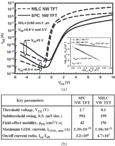
Fig. 2(a) shows the typical transfer characteristics of the proposed NW TFTs with MILC and SPC poly-Si channels at
VDS= 0.5 and 3 V. The TFT device composed from a couple of NW channels has a nominal channel length (L) of 1 µm and an effective channel width (W ) of 100 nm (2× WSi). The threshold voltage (VTH), subthreshold swing, and field-effect mobility were extracted at VDS= 0.5 V, whereas the maxi-mum off-state GIDL current (IGIDL,max) and on/off current ratio (Ion/Ioff) were extracted at VDS= 3 V. The threshold voltage was defined as the gate voltage required to achieve a normalized drain–current of IDS= (W/L)× 100 nA. The
Fig. 2. (a) Comparison of transfer characteristics for the MILC and SPC NW TFTs with L = 1 µm and W = 2× 50 nm. The inset shows ln[IDS/(VGS−
VFB) versus 1/(VGS− VFB)2 curves at VDS= 0.5 V and the extracted
effective trap state density. (b) Comparison of device characteristics for the MILC and SPC NW TFTs.
key device parameters are shown in Fig. 2(b). Accordingly, the threshold voltage and the subthreshold swing of the MILC NW TFT are 0.1 V and 199 mV/dec, respectively, which are superior to 2.7 V and 594 mV/dec of the SPC NW TFT. Notably, the maximum GIDL current of the MILC NW TFT is more than one order in magnitude lower than that of the SPC NW TFT. The on/off current ratio of the MILC NW TFT (4.7× 10⁷) is much higher than that of the SPC NW TFT (3.2× 10⁶). Additionally, the MILC NW TFT has an obvious enhancement in the maximum field-effect mobility from 42 to 156 cm2/V· s, as compared to the SPC NW TFT. Note that the major performance improvements in the MILC NW TFT are due to the alignment of poly-Si grains in a direction that is parallel to the current flow. Also, the growth of poly-Si grains perpendicular to the channel direction is effectively limited by the nanoscale channel width of 50 nm. Therefore, the effects of parallel grain boundaries could be relieved by decreasing the channel width to be comparable to or even smaller than the poly-Si grain size. However, the grain boundaries are randomly oriented in the SPC NW TFT.
In order to verify the reduction of grain-boundary defects in the MILC poly-Si, the effective trap state density (Ntrap) was calculated from the square root of the slope of ln[(IDS/(VGS−
VFB)] versus 1/(VGS− VFB)2 plot, which was proposed by Proano et al. [15], as shown in the inset of Fig. 2(a). It is observed that the MILC NW TFT shows a much reduced
476 IEEE ELECTRON DEVICE LETTERS, VOL. 29, NO. 5, MAY 2008
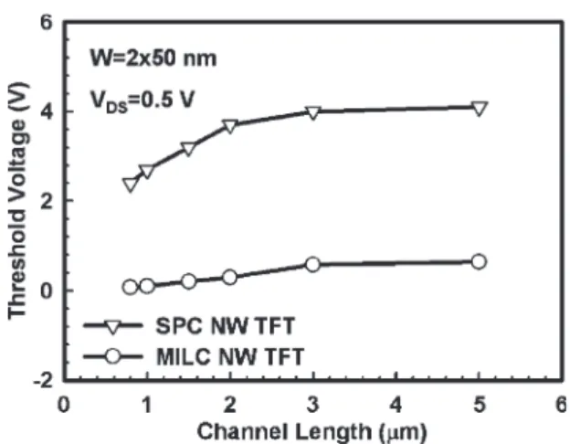
Fig. 3. Threshold-voltage rolloff properties of the MILC and SPC NW TFTs with channel lengths (L’s) varying from 5 µm to 0.8 µm; the channel widths (W ’s) are kept at 2× 50 nm.
effective trap state density from 1.13× 10¹³ to 5.67× 1012 cm−2 as compared to the SPC NW TFT. This figure strongly implies that the MILC technique can obtain a good-quality poly-Si film with a larger grain size and fewer micro-structural defects.
Additionally, to examine the grain crystallinity of poly-Si NWs with different crystallization techniques, the threshold-voltage rolloff properties of the MILC and SPC NW TFTs are shown in Fig. 3. Apparently, the SPC NW TFT exhibits a serious threshold-voltage rolloff property, which is dominated by the decrease of randomly distributed grain boundaries con-tained in the channel [16]. However, a much more improved scaling characteristic is observed in the MILC NW TFT, which could be ascribed to the fabrication of an entire device on a nearly single-crystal grain; therefore, compared to the SPC NW TFT, the MILC NW TFT could not only relieve the effects of grain boundaries but also achieve a lower threshold voltage.
IV. CONCLUSION
We have proposed a novel high-performance poly-Si TFT with 50-nm NW channels crystallized by the MILC tech-nique. The experimental results show that the proposed MILC NW TFT not only depicts improved turn-on characteristics by forming good-quality poly-Si films as well as superior triple-gate controllability over the NW channel potential but also maintains a low off-state leakage current by reducing the microstructural defects. Superior short-channel characteristics are also achieved, which might be explained by the formation of single-crystal grains in the entire channel region. Therefore, the proposed MILC NW TFT could be indeed suitable for imple-menting low-cost, high-density, and high-performance driver circuits on the glass panel for AMLCD applications.
ACKNOWLEDGMENT
The authors would like to thank National Nano Device Labo-ratories and the Nano Facility Center, National Chiao Tung University for the apparatus support.
REFERENCES
[1] I. W. Wu, “Cell design considerations for high-aperture-ratio direct-view and projection polysilicon TFT-LCDs,” in Proc. SID Dig. Tech. Papers, 1995, pp. 19–22.
[2] H. Kuriyama, Y. Ishigaki, Y. Fujii, S. Maegawa, S. Maeda, S. Miyamoto, K. Tsutsumi, H. Miyoshi, and A. Yasuoka, “A C-switch cell for low-voltage and high-density SRAMs,” IEEE Trans. Electron Devices, vol. 45, no. 12, pp. 2483–2488, Dec. 1998.
[3] M. Cao, S. Talwar, K. J. Kramer, T. W. Sigmon, and K. C. Saraswat, “A high-performance polysilicon thin-film transistors using XeCl excimer laser crystallization of pre-patterned amorphous Si films,” IEEE Trans.
Electron Devices, vol. 43, no. 4, pp. 561–567, Apr. 1996.
[4] H. Wang, M. Chan, S. Jagar, V. M. C. Poon, M. Qin, Y. Wang, and P. K. Ko, “Super thin-film transistor with SOI CMOS performance formed by a novel grain enhancement method,” IEEE Trans. Electron Devices, vol. 47, no. 8, pp. 1580–1586, Aug. 2000.
[5] V. W. C. Chan, P. C. H. Chan, and C. Yin, “The effects of grain boundaries in the electrical characteristics of large grain polycrystalline thin-film transistor,” IEEE Trans. Electron Devices, vol. 49, no. 8, pp. 1384–1391, Aug. 2002.
[6] V. W. C. Chan and P. C. H. Chan, “An empirical model to determine the grain size of metal-induced lateral crystallized films,” IEEE Trans.
Electron Devices, vol. 49, no. 8, pp. 1399–1404, Aug. 2002.
[7] Y. C. Wu, T. C. Chang, P. T. Liu, C. S. Chen, C. H. Tu, H. W. Zan, Y. H. Tai, and C. Y. Chang, “Effects of channel width on elec-trical characteristics of polysilicon TFTs with multiple nanowire chan-nels,” IEEE Trans. Electron Devices, vol. 52, no. 10, pp. 2343–2346, Oct. 2005.
[8] H. C. Lin, M. H. Lee, C. J. Su, and S. W. Shen, “Fabrication and char-acterization of nanowire transistors with solid-phase crystallized poly-Si channel,” IEEE Trans. Electron Devices, vol. 53, no. 10, pp. 2471–2477, Oct. 2006.
[9] M. C. Lemme, C. Moormann, H. Lerch, M. Moller, B. Vratzor, and H. Kurz, “Triple-gate metal-oxide semiconductor field effect transistors fabricated with interference lithography,” Nanotechnology, vol. 15, no. 4, pp. S208–S210, Apr. 2004.
[10] Z. Xiong, H. Liu, C. Zhu, and J. K. O. Sin, “A new polysilicon CMOS self-aligned double-gate TFT technology,” IEEE Trans. Electron Devices, vol. 52, no. 2, pp. 2629–2633, Dec. 2005.
[11] S. Miyamoto, S. Maegawa, S. Maeda, T. Ipposhi, H. Kuriyama, T. Nishimura, and N. Tsubouchi, “Effect of LDD structure and channel poly-Si thinning on a gate-all-around TFT (GAT) for SRAMs,” IEEE
Trans. Electron Devices, vol. 46, no. 8, pp. 1693–1698, Aug. 1999.
[12] C. W. Chang, C. K. Deng, H. R. Chang, C. L. Chang, and T. F. Lei, “A simple spacer technique to fabricate poly-Si TFTs with 50-nm nanowire channels,” IEEE Electron Devices Lett., vol. 28, no. 11, pp. 993–995, Nov. 2007.
[13] T. Uchida, “Present and future trend of electron device technology in flat panel display,” in IEDM Tech. Dig., 1991, pp. 5–10.
[14] J. W. Yang and J. G. Fossum, “On the feasibility of nanoscale triple-gate CMOS transistors,” IEEE Trans. Electron Devices, vol. 52, no. 6, pp. 1159–1164, Jun. 2005.
[15] R. E. Proano, R. S. Misage, and D. G. Ast, “Development and elec-trical properties of undoped polycrystalline silicon thin-film transis-tors,” IEEE Trans. Electron Devices, vol. 36, no. 9, pp. 1915–1922, Sep. 1989.
[16] S. Chopra and R. S. Gupta, “An analytical model for current-voltage char-acteristics of a small-geometry poly-Si thin-film transistor,” Semicond.