國立交通大學
電子工程學系電子研究所碩士班
碩士論文
動態調整頻率產生器與能量效率最佳化單位應用在太
陽能電源管理系統
Dynamic Frequency Scaling Clock Generator and Power
Efficiency Optimization Unit for Solar Cell Power
Management System Application
研究生:闞之晧
指導教授:黃威教授
中華民國九十七年六月
中華民國九十七年六月
中華民國九十七年六月
中華民國九十七年六月
動態調整頻率產生器與能量效率最佳化單位應用在太
陽能電源管理系統
Dynamic Frequency Scaling Clock Generator and Power
Efficiency Optimization Unit for Solar Cell Power
Management System Application
研究生:闞之晧 Student:Chih-Hao Kan
指導教授:黃威教授 Advisor:Prof. Wei Hwang
國立交通大學
電子工程學系電子研究所
碩士論文
A Thesis
Submitted to Department of Electronics Engineering & Institute of Electronics College of Electrical Engineering and Computer Engineering
National Chiao Tung University in partial Fulfillment of the Requirements
for the Degree of Master
in
Electronics Engineering June 2008
Hsinchu, Taiwan, Republic of China
中華民國九十七年六月
中華民國九十七年六月
中華民國九十七年六月
動態調整頻率產生器與能量效率最佳化單位應用在太
陽能電源管理系統
研究生:闞之晧 指導教授:黃威教授
國立交通大學電子工程學系電子研究所
摘要
隨著手持裝置的廣泛應用, 低功率成為電路設計的主要考量之ㄧ; 同時隨著先 進製程的使用, 數位取代傳統類比電路也逐漸成為趨勢。 本論文研究數位形式 的頻率產生器, 提出了一個雙輸出的數位頻率產生器, 每個輸出都可以隨意調 整頻率和相位, 總共有六種頻率倍數可以選擇。 此數位頻率產生器利用了平穩 充電相位合成器來增加相位資訊, 低功率的延遲單位使延遲線消耗較少的功率, 同時利用數位充電控制器來快速分辨頻率和延遲來達到快速鎖定。 本論文也研 究低電壓震盪器, 並利用低電壓震盪器在能量效率最佳化單位。 能量效率最佳 化單位可以依據不同負載的情況來動態調整供應給1V產生器的時脈頻率, 來達 到能量效率的最佳化。 能量效率最佳化單位應用在太陽能電源管理系統, 此系 統接收太陽能源並且輸出500mV、-500mV 以及1V 給運算電路及記憶體電路。這 個系統在白天由太陽能源提供能量, 在黑夜由電池提供能量。所有研究使用UMC 90nm CMOS 技術實現。Dynamic Frequency Scaling Clock Generator and Power
Efficiency Optimization Unit for Solar Cell Power
Management System Application
Student:Chih-Hao Kan Advisor:Prof. Wei Hwang
Department of Electronics Engineering & Institute of Electronics
National Chiao-Tung University
ABSTRACT
The portable device has been widely used, the low power consumption has become the main concern of circuit design; and the deep-submicron process also bring the trend of replacement of analog intensive architectures with more digital ones. This thesis proposed a digital dual output clock generator with dynamic frequency/phase tuning ability. Each output is independent when tuning frequency and phase and total six multiplied factors are available. The proposed clock generator uses smooth charge phase blender to increase the phase information. The low power delay cell saves the power consumption and the digital charge-detecting controller can achieve fast lock. The low voltage oscillators also had been researched and used it in power efficiency optimization unit. The power efficiency optimization unit supplies a variable frequency (33MHz~300MHz) clock to 1V generator according to the loading condition. The unit is applied in the solar cell power management system. The system accepts power from photovoltaic cell and outputs 500mV, -500mV and 1V to computation circuit and memory circuit. In daytime, the power management is supplied by solar energy and the battery is charged. At night, the battery will supply energy to power management system. All research is implemented in UMC 90nm CMOS technology.
致謝
我要感謝指導教授黃威老師,老師指導了我研究的方向,同時也教導了我許 多知識,更開拓了我研究領域的視野。老師提供了一個優良且舒適的的研究環境 與充足的研究資源,讓我能夠充分利用來完成這一篇論文。 我也要特別感謝張銘宏學長,帶領我接觸我的研究領域並教導我許多知識與 道理,讓我能夠完成這篇碩士論文的研究。 同時我也要感謝黃柏蒼、謝維致和楊皓義學長對於我在研究上的幫助與鼓 勵。 最後我要感謝我其他的實驗室夥伴、我的朋友、與我的家人,對我的關懷幫 助以及精神上的支持,讓我能夠順利的完成碩士的論文研究。Contents
Chapter 1
Introduction...1
1.1 Research Motivation ...2 1.2 Thesis Organization ...3Chapter 2
PLL/DLL Design Concepts ...5
2.1 Introduction...5 2.2 The Architecture of PLL ...6 2.2.1 Analog PLL...6 2.2.2 All Digital PLL ...7 2.3 The Architecture of DLL ...8 2.3.1 Analog DLL ...8 2.3.2 All Digital DLL...102.4 The Common Block Circuits ...10
2.4.1 Phase Detector ...10
2.4.2 Charge Pump...12
2.4.3 Loop Filter ...14
2.4.4 Time to Digit Converter ...14
2.4.5 Oscillator/Delay Line...16
2.4.5 Frequency Divider ...19
2.5 PLL/DLL System Noise Analysis and Design Technique ...20
2.5.1 PLL/DLL rms Jitter Analysis ...21
2.5.2 Impedance Level Scaling Technique ...25
2.5.3 Analysis of PLL Jitter Caused by Digital Switching Noise...27
Chapter 3
Overview of Dynamic Frequency Scaling Technique and Proposed
Dual Output Clock Generator with Dynamic Frequency/Phase
Tuning Ability...33
3.1 Dynamic Frequency Scaling System ...33
3.1.1 The Dynamic Frequency Scaling Technique ...34
3.2 Proposed Dual Output Clock Generator with Dynamic Frequency/Phase Tuning Ability ...39
3.2.1 The Architecture of Proposed Clock Generator...40
3.2.3 Low power six-phase delay-locked loop ...57
3.2.4 Simulation Result of the Proposed Clock Generator ...62
3.3 Conclusion of Proposed Clock Generator and Application in Advance Power Management System...66
Chapter 4
Low Voltage Oscillators with Wide Tuning Range ...69
4.1 Introduction to Low Voltage Circuit Design...69
4.2 The Type I Low Voltage Differential Oscillator with Wide Tuning Range ………..70
4.3 The Net-Bias Circuit ...76
4.4 The Type II Low Voltage Oscillator with Wide Tuning Range ...77
Chapter 5
The Application of Power Efficiency Optimization Unit in Solar Cell
Power Management System ...85
5.1 The Solar Cell Power Management System ...86
5.2 The Power Efficiency Optimization Unit ...90
5.3 The Simulation Results of Power Efficiency Optimization Unit and the Solar Cell Power Management System………94
Chapter 6
Conclusion and Future Work ...102
6.1 Conclusion ...102
6.2 Future Work ...103
List of Figures
Fig 2.1 The architecture of analog PLL………6
Fig 2.2 The architecture of all digital PLL....………...…8
Fig 2.3 The architecture of analog DLL………..…….9
Fig 2.4 (a) Conventional phase frequency detector (b) Timing diagram…….10
Fig 2.5 NAND gates style conventional phase frequency detector…………...11
Fig 2.6 the state diagram………..12
Fig 2.7 charge pump……….12
Fig 2.8 (a) Single-end charge pump (b) NMOS charge pump………..13
Fig 2.9 (a) 1st order loop filter (b) 2nd order loop filter (c) 3rd order loop filter………...14
Fig 2.10 Time-to-digital converter (TDC): (a) Structure (b) Quantization of the timing difference between the DCO and FREF edges………..…15
Fig 2.11 2 level time-to-digital converter (TDC) structure………...16
Fig 2.12 Typical voltage controlled LC oscillator………..17
Fig 2.13 Differential CML type gain block oscillator………17
Fig 2.14 Differential gain block………...………18
Fig 2.15 Binary weighted digital controlled differential delay cell…………19
Fig 2.16 Varactor style delay cell using NAND gate………..19
Fig 2.17 The basic /4/5 two mode divider………...20
Fig 2.18 Concept of impedance level scaling………..25
Fig 2.19 Effect of impedance level scaling………..26
Fig 2.20 Noise generated by digital logic couples through the substrate to an analog circuit………..……….…27
Fig 2.21 Three power supply schemes under investigation. (a) PLL0: common Vdd and Vss , (b) PLL1: separate analog Vdd , (c) PLL2: separate analog Vdd and Vss……….…………29
Fig 2.22 Jitter measurement with PLLs having a bandwidth of 4 MHz…….30
Fig 2.23 Triple-well processing provides a buried well that breaks the resistive noise coupling path………..31
Fig 2.24 Jitter induced by NG31 into PLLs having a bandwidth of 4 MHz. Prefix 3W indicates that the block resides in a triple-well... .…….32
Fig 3.1 Conventional EPIC architecture and multiple clock domain EPIC...35
Fig 3.3 The performance comparison……….38
Fig 3.4 The EDP comparison………...39
Fig 3.5 The architecture of proposed dual output clock generator with dynamic frequency/phase tuning ability……….……..………41
Fig 3.6 The conventional phase blender………..………43
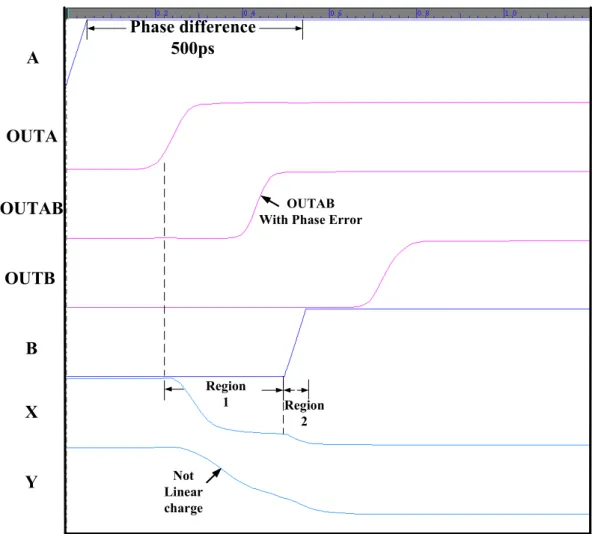
Fig 3.7 The smooth charge phase blender (SCPB)………44
Fig 3.8 The voltage curve of SCPB when phase difference is 400 ps……..45
Fig 3.9 The performance comparison of SCPB and conventional phase blender………..46
Fig 3.10 The voltage curve of SCPB when phase difference is 500 ps……….47
Fig 3.11 The modified dynamic controlled SCPB……….………..………..48
Fig 3.12 The performance of the modified SCPB…………...………..49
Fig 3.13 The architecture of the DDPS………..………….………...50
Fig 3.14 The clock multiplier and duty cycle circuit proposed in [34]….……51
Fig 3.15 The edge combiner………..52
Fig 3.16 The toggle pulsed latch………...53
Fig 3.17 The two examples of frequency synthesis…………...………..54
Fig 3.18 The rising edge pulse scheme to handle the 50% duty cycle………….56
Fig 3.19 The low power delay cell………..………...57
Fig 3.20 The control signal to select coarse stage...58
Fig 3.21 The digital charge-detecting controller (DCD controller)………..59
Fig 3.22 The charge-detecting line (CDL)………60
Fig 3.23 The detecting condition of coarse tune signals………..61
Fig 3.24 The locking procedure……….64
Fig 3.25 The output frequency of six multiplied factors...65
Fig 3.26 The dual clock output and dynamic frequency scaling example……….66
Fig 3.27 The advance power management concept……….68
Fig 4.1 The proposed type I low voltage delay cell...70
Fig 4.2 General voltage controlled delay cell………...72
Fig 4.3 Type I oscillator with 7 stages………...72
Fig 4.4 The delay time of the proposed type I low oscillator using different control step……….73
Fig 4.5 The output frequency of the proposed type I low oscillator using different control step……….74
Fig 4.6 The range of frequency and delay time of proposed type I low voltage oscillator with different power supply voltage ...75
Fig 4.7 The net-bias circuit...76
Fig 4.8 The proposed type II low voltage oscillator………77
Fig 4.9 (a) The delay time of the proposed type I low oscillator using different control step (b) The output frequency of the proposed type I low oscillator using different control step...79
Fig 4.10 The range of frequency and delay time of proposed type II low voltage oscillator with different power supply voltage ...80
Fig 4.11 The power consumption of proposed type II low voltage oscillator with small inverter sizes……….81
Fig 4.12 The non-full swing condition when oscillator operates at low frequency.. ………..82
Fig 4.13 The power consumption of proposed type II low voltage oscillator with big inverter sizes……….83
Fig 4.14 The power consumption comparison with different oscillators ...84
Fig 5.1 The solar cell power management system………..87
Fig 5.2 The control unit………..88
Fig 5.3 The voltage level of output of regulator and output of 1V generator in the condition of loading increase and PV cell power reduce gradually……...88
Fig 5.4 The architecture of power efficiency optimization unit……….91
Fig 5.5 The oscillating voltage detector………92
Fig 5.6 The detecting point of oscillating voltage detector versus different temperature conditions...93
Fig 5.7 The bias voltage detector………...94
Fig 5.8 The power efficiency measurement of the 1V generator………95
Fig 5.9 The power efficiency of the 1V generator (oscillating voltage detector)..96
Fig 5.10 The power efficiency of the 1V generator (bias voltage detector)……...97
Fig 5.11 The three different output voltage with variation of current from PV cell ………..98
Fig 5.12 Comparison of power management system with CU and without CU...99
Fig 5.13 The layout view of solar cell power management system………...100
List of Tables
Table I Frequency/Phase combination and program signals……….55 Table II The performance of proposed clock generator………...63 Table III Power management system for solar energy harvesting………….100
1
Chapter 1
Introduction
The need for low cost, low power communication systems has motivated the use of deep-submicron CMOS processes. Technology scaling improves digital blocks, but complicates the design of RF and analog circuits. Thus the replacement of analog intensive architectures with more digital ones will become unavoidable. Analog frequency synthesizers are used in both wireless transceivers and wire line digital links. Recently All Digital Phase-Locked Loop (ADPLL) and All Digital Delay-Locked Loop (ADDLL) have appeared featuring good scalability, programmability and robustness but performance still inadequate for high end applications.
The PLL and DLL are very important clocking IPs for many digital systems such as digital communication and microprocessor. The PLL has been widely used for digital system, communication system and interconnection system. It can be used to eliminate the delay between external and internal clock signals caused by the on-chip clock delay. Among the main applications of PLLs are noise and jitter suppression in communications, skew suppressions in digital systems, data synchronization between chips, and frequency synthesis in RF transceivers. DLLs are also widely used as de-skew buffers and clock generators in microprocessors, DSPs, multi-core SoCs , DRAM interfaces and application-specified integrated circuits. In recent years, the DLL has become an important component for safe clocking of SoCs with block-based power-down mechanism, and thus low power, small jitter, and fast lock-in become three equally important design goals.
2
Compared to most phase-locked-loop-based clock generators and local oscillators, delay-locked loop-based counterparts exhibit less jitter and phase noise because of no jitter accumulation. This is true even under severe supply noise which is becoming common and critical in many SoCs. Furthermore, they show stable operation with process, voltage and temperature (PVT) variations, are easier to design, and occupy smaller area due to a simpler loop filter.
1.1
Research Motivation
In this thesis, a dual output clock generator with dynamic frequency/phase tuning ability is proposed first. It generates two independent clock signal sources, and the architecture is extensible to provide more sources. Two low voltage oscillators with wide tuning range are researched for applied in solar cell power management system. Finally the power efficiency optimization unit using low voltage oscillator is developed and applied to the solar cell power management system.
The fast growing IC industry makes the trend of more complicate system integration and minute operation. The dynamic frequency scaling technique is widely used in system power management aspect. Huge demand of multiple clock domain are also be desired by multi-core system, which need a clock generator capable of multi-frequency/phase ability to operate. Under this demand, clock generator with multiple clock outputs and dynamic frequency/phase tuning ability is essential for system aspect and power management.
The research motivation of proposed dual output clock generator with dynamic frequency/phase tuning ability is make the clock generator more capable of the trend of multi clock domains and dynamic scaling. The advance power management concept is also proposed as the application concept of multi outputs clock generator.
3
In the recent years, the market of portable devices likes notebook, cell phone, PDA and smart phone is grow up rapidly and more new portable products will be developed in the near future. In the developing of portable devices, more and more functions are integrated into a product. At the same time, people concern that whether the product can use for a long time without charging the battery in charge socket. Recently, the price of oil keeps going up. This will impact the electric bill and cost of expense. To increase the utility time and lower the cost of expense, the low power techniques are urgent need. In alternative way, people look for the new alternative energy actively. Environmental energy like solar power, heat power and wind power is used for generating electric power. Due to energy crisis and eco-awareness, the research of energy harvesting application is getting popular.
The energy harvesting system of the solar cell power management system is proposed by me and Tung-Hau Tsai as the energy platform power by solar cell. The efficient power management system harvest energy from the solar and transfer it efficiently to computation circuit and battery. The power efficiency optimization unit is also proposed to optimize the power efficiency of 1V generator according to the loading condition. The solar cell power management system is proposed in the trend of neutral energy harvesting.
1.2
Thesis Organization
The thesis is organized as follows:
Chapter 2 gives the PLL/DLL design concepts. Including the architecture of analog/digital PLL/DLL, and the block circuit is introduced.
Chapter 3 introduces the dynamic frequency scaling system and proposed dual output clock generator with dynamic frequency/phase tuning ability. The advance power
4
management concept is also presented.
Chapter 4 introduces two low voltage oscillators with wide tuning range, which is researched to use in power efficiency optimization unit. The power efficiency optimization unit is applied to solar cell power management system.
Chapter 5 presents the power efficiency optimization unit and the solar cell power management system. The simulation results and layout also implemented and be presented.
5
Chapter 1
PLL/DLL Design Concepts
2.1
Introduction
Clock source is essential circuit block in digital circuits, since every digital circuit needs clock to trigger. The performance and stability of clock source has great impact to circuit operation. Although the clock source, like PLL, had been widely researched for a long time, the increasing operation frequency and more complicated system brings new challenges to clock source, include more widely frequency range supply, low jitter, low power consumption, dynamic scaling, even the fast locking. The advance deep-sub-micro process also gives more challenges to mix-signal and analog intensive circuits design, thus makes all digital style clock generator become popular.
In this chapter, the conventional PLL/DLL design concepts will be discussed, Include the architecture of both structures and circuit design. The common issue of PLL/DLL will also be discussed.
In section 2.2, the architecture of PLL will be shown; also the analog type and digital type PLL will be studied. The difference of two types will be presented. In section 2.3, the architecture of DLL will be shown.
Several common block circuits will be studied in section 2.4. Phase detector which is used to capture phase difference between two signals will be studied in section 2.4.1. Charge pump is an essential circuit in analog style voltage control PLL/DLL, and time-to-digit converter is also very important circuit in digital style PLL/DLL, both will studied in section 2.4.2 and section 2.4.3.
6
In both PLL/DLL, the oscillator/delay cell is the key of entire circuits. Most of the jitter sources are contributed by this blocks, the range of frequency also bounds by it, and over 50% power consumption come from oscillator/delay cell. The studied of oscillator/delay cell will presented in section 2.4.4. The divider which used in some architecture will be studied in section 2.4.5.
Finally the common issue in all PLLs/DLLs will studied in section 2.5, include power issue and jitter issue.
2.2
The Architecture of PLL
2.2.1 Analog PLL
Phase-locked loop (PLL) is a very important clocking IP for many digital systems such as digital communication and microprocessor. It can be used for frequency synthesis, clock de-skew, and duty-cycle enhancement. The typical PLL used negative feedback loop to synchronize the output clock and the reference clock. Fig 2.1 shows the architecture of analog PLL. There are phase detector(PD) or phase frequency detector(PFD), charge pump(CP), loop filter(LPF), voltage control oscillator(VCO), and frequency divider(/N). If the PLL was locked, the phase and frequency of two periodic input signals of PD were ideally the same, and the frequency of the output of VCO(fout) will be N times of reference clock.
PD
CP
LPF
VCO
/N
fout
ref
7
Just like most analog circuits, the analog PLL shows superior performance over digital style PLL, especial in output frequency range. But the design of analog loop needs more effort, the loop have to be convergent. The analog circuit is sensitive to noise, thus brings the hard working condition in deep-sub-micro process. The analog feature make analog PLL can not be portable with process, and any change to the spec will easily lead to redesign the whole loop. These drawbacks lead digital style PLL to rise and widely use in many applications.
2.2.2 All Digital PLL
The advance technology makes system design to be more integrated. The system-on-chip(SOC) makes traditional circuit design to become system design, and mostly digital systems. Integrating an analog block into a digital system needs to take more design efforts, and also the deep-sub micro process environment is unfriendly to analog designs, all of these give the rising of all digital style PLL.
In a deep-submicron CMOS process, time-domain resolution of a digital signal edge transition is superior to voltage resolution of analog signals. Thus the ADPLL has the higher immunity for switching noise, and process, voltage and temperature (PVT) variations. The ADPLL can be ported to different process as a soft intellectual property (IP), and make it can be easily integrated into the system. And it also shows the better testability, programmability, and stability.
The architecture of standard all digital PLL is shown in Fig 2.2[1]. As Fig 2.2(a), there are phase detector(PD) or phase frequency detector(PFD), direction circuit, up/down counter, digitally controlled oscillator(DCO), and frequency divider(/N). The direction circuit and up/down counter can be replaced by time-to-digit converter(TDC), as Fig 2.2(b).
8
The direction circuit can provide signal that decide the “lead” or “lag” condition between two input signals of PD, then up/down counter tracing the direction signal until the output of DCO is synchronized to the reference clock. The time-to-digit converter can form analog timing condition directly to digital oscillator controlled signals. The loop function is just like analog PLL, but each block circuit is replaced by the digital one.
2.3
The Architecture of DLL
2.3.1 Analog DLL
9
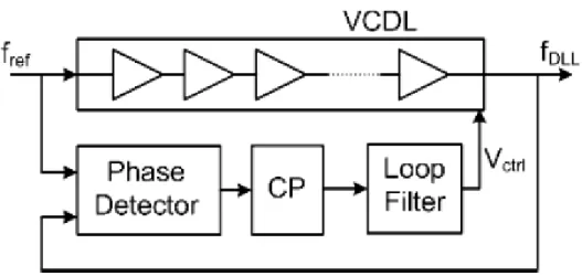
The delay-locked loop(DLL) is another widely used clocking source for clock de-skew, clock synchronize, and clock synthesis. Unlike PLL, the operation of DLL is used delay line to delay reference clock, when the total delay of delay line is one reference cycle, the DLL is locked, and the reference clock and the output of delay line is synchronized.
Fig 2.3 shows the architecture of analog DLL. There are phase detector(PD) or phase frequency detector(PFD), charge pump, loop filter, and voltage controlled delay line(VCDL). The main difference of architecture between DLL and PLL is the delay line in the DLL did not form a loop which as oscillator of PLL, it simply delayed the input reference clock. The basic function of the rest component is the same as in the PLL.
The most attractive feature of DLL is the jitter reduction, comparing to PLL, DLL shows better jitter performance over PLL since no jitter accumulation.
10
2.3.2 All Digital DLL
The all digital delay-locked loop (ADDLL), like all digital phase-locked loop (ADPLL), is a DLL using digital component. There are phase detector (PD) or phase frequency detector (PFD), tine-to-digit converter (TDC), and digital controlled delay line (DCDL). Except TDC scheme, there are counter-controlled based scheme, D flip-flop scheme, binary search scheme, and successive approximation register controlled scheme (SAR).
2.4
The Common Block Circuits
2.4.1 Phase Detector
There are several considerations when design a phase detector or a phase frequency detector, one is the minimum detectable phase error, another is the maximum operation frequency, the linear characteristic is also very important. Fig 2.4(a) shows the conventional phase frequency detector, it was consist of two D flip-flop and a AND gate. The timing diagram is shown in Fig 2.4(b), the “lead” and “lag” condition will be quantified to DOWN and UP signals. The UP and DOWN signals thus can provide the direction and value of phase condition.
11
Fig 2.5 shows another conventional phase frequency detector using nine NAND gates, and the state diagram is shown in Fig 2.6. Several issue of this PFD should be considered, there are glitch, dead-zone, and maximum operation frequency limit. To the glitch, there are two ways to reset UP signals, from point X to UP or from point Y to UP. To avoid glitch, it can insert more delay on point X to match the delay of point Y. Even the REF and FBAK is at the same phase, the minimum pulse still will happen at UP and DOWN signals. Insert more delay at the output of NAND gates can increase the width of the minimum pulse, but maximum operation frequency of the PFD will also be limited.
12
2.4.2 Charge Pump
Charge pump is used to convert the PD output signals, usually the UP, DOWN signals, to the controlled voltage. The basic concept of charge pump is shown in Fig 1.7. The UP, DOWN signals works as a switch, through the switch the current Ip will charge or discharge the control voltage (Vctrl), which is going to control the oscillator in the PLL or the delay line in the DLL.
Fig 2.6 the state diagram
13
In the analog CMOS switch and dynamic digital circuits there are many undesirable effects, like charge sharing and current leakage. In the charge pump the switch current could exceed the UP/DOWN controlled main current due to the charge sharing. When the PLL or DLL was locked and stable, PFD still generating the minimum width pulse UP/DOWN signals, suppose the width of the pulse is ts, the current mismatch(∆I) could be happened due to channel length modulation, the offset charge(DQ) will be DQ=(Iup-Idn)*ts. DQ will introduce static offset phase error, to minimum this error, the current mismatch of UP/DOWN switch should be minimum.
There several conventional charge pump circuits, Fig 2.8(a), this is single-end charge pump, and the switch is on the drain of the current mirror. When DN opened, the drain voltage of M1 will be low, when DN connected, the drain voltage of M1 will rise to output control voltage. M1 will operate at linear region, until the drain voltage was high enough to put M1 into saturated region. There should be noticed that the charge sharing effect could be happened at the drain node of M1 and M2. Fig 2.8(b) shows another conventional charge pump. It used current mode circuit to achieve high operation speed. Because of the constant bias current, the voltage noise could be reduced. It only used NMOS switch to prevent the current mismatch between NMOS and PMOS.
14
2.4.3 Loop Filter
Analog style PLL or DLL used loop filter to convert the current signal of the charge pump’s output to the voltage signal, and it filtered the high frequency noise. Fig 2.9 shows the first order, second order, and third order loop filter. The design of loop filter should consider the stability of the loop and the operation frequency. The passive component will occupy lots of area, especially capacitor. Area issue should be noticed when design loop filter.
2.4.4 Time to Digit Converter
The time to digit converter (TDC) is used in ADPLL or ADDLL to convert timing information directly to the digital code. The TDC usually consist of the delay that is identical or multiple or fractional to the single delay cell in the delay line or oscillator, the concept is let timing signal to pass this delay then extracting the information to the digital code.
Fig 2.10(a) shows the structure of a TDC[2]. It consists of several inverters to form the delay. There are flip-flops connect to each output of inverters, and operated with high frequency. The timing signal pass the delay line consists of the inverters with high frequency flip-flops to sample the information, and converted to the digital code. Since the conventional phase/frequency detector
15
and charge pump are replaced by the TDC, the phase-domain operation does not fundamentally generate any reference spurs thus allowing for the digital loop filter to be set at an optimal performance point between the reference phase noise and oscillator phase noise. Fig 2.10(b) shows quantization of the timing difference between the DCO and reference clock edges.
Level structure technique could reduce circuit complexity and area. Fig 2.11 shows the two levels TDC[3]. There are several functional blocks, namely one long delay chain, one short delay chain, 1st level flash TDC, 2nd level flash TDC, path selection multiplexer, and cycle time calculator. The long delay chain consists of 32 delay cells, and these delay cells are partitioned into four sections
Fig 2.10 Time-to-digital converter (TDC): (a) Structure (b) Quantization of the timing difference between the DCO and FREF edges
16
(Secs.0-3). In contrast to long delay chain, the short delay chain has only 8 delay cells. All delay cells used in long and short delay chain remain the same as those for DCO coarse-tuning stage. When the TDC is enabled, Ref N is sent to the long delay chain, and all outputs (DL [3:0]) are sent to the 1st level flash TDC. When the first falling edge of Ref N arrives, the 1st level flash TDC generates the section selection signal (Li_SEL) to select one of section outputs for the short delay chain. Then the 2nd level flash TDC generates the delay selection signal (L2 SEL) based on the delay outputs (BL[7:0]). The section and delay outputs are thermometer code type that can be used to generate selection signals easily. When both LI SEL and L2_SEL have been generated, the cycle time calculator can estimate the period of Ref N. The conversion equation can be given as
Tr= (LI _SEL x8+L2 SEL) x2 (1) Where Tr is the period of Ref N.
2.4.5 Oscillator/Delay Line
The oscillator is constructed by the LC oscillator or several delay cells to form the loop. Traditional analog PLL used LC-tank style oscillator, as shown in Fig 2.12, it’s a typical voltage controlled LC oscillator. The LC oscillator under certain voltage condition could generate a sin wave. The LC oscillator has superior performance, but the analog characteristic make it hard to design in deep-sub micro environment, and the passive component would occupy huge area.
17
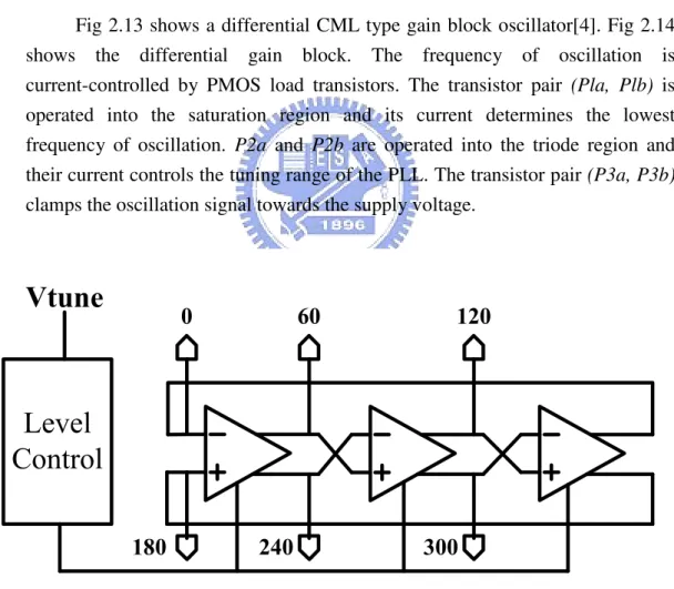
Fig 2.13 shows a differential CML type gain block oscillator[4]. Fig 2.14 shows the differential gain block. The frequency of oscillation is current-controlled by PMOS load transistors. The transistor pair (Pla, Plb) is operated into the saturation region and its current determines the lowest frequency of oscillation. P2a and P2b are operated into the triode region and their current controls the tuning range of the PLL. The transistor pair (P3a, P3b) clamps the oscillation signal towards the supply voltage.
Vc
Vc
Fig 2.12 Typical voltage controlled LC oscillator
Level
Control
Vtune
180
240
300
0
60
120
18
To the digital controlled delay cells, there are delay cells used one transistor to realize the tuning capacitance, but it will limited the native resolution to the smallest transistor achievable by a process. The native resolution can be refined by increasing the driving strength, but the power consumption will be increased.
Fig 2.15 shows the binary weighted digital controlled differential delay cell[5]. One path comprises of a fixed capacitance realized with the minimum-sized transistor and the other path comprises of a tuning capacitance that is realized by adjusting the size of transistor. The difference of capacitance determines the finest delay resolution, which can be made sufficiently small. The BWDC also has two distinct features that contribute to low power. First, there is no need for large driving and so logic gates can be minimally sized. Second, the de-multiplexing gates are placed at the input side so that only the components in one path are activated.
19
Except MOS capacitor style digital controlled delay cell, there are also NAND gate style digital controlled varactor(DCV)(all dpll optical). Fig 2.16 illustrates a varactor cell using a two-input NAND gate. The gate-to-channel capacitance contributes to total gate capacitance. This method controls the capacitance between gate and source or between gate and drain. The NAND gate capacitance at CL depends on the value of the Bctr.
2.4.5 Frequency Divider
Frequency divider used in PLL to divide VCO or DCO output frequency. The synchronized divider will consume very high power, and it need high frequency respond. Practically PLL used two-mode divider to down the system
Fig 2.15 Binary weighted digital controlled differential delay cell
20
speed.
Fig 2.17 shows the basic /4/5 two mode divider. It consists of three D flip-flops and two NAND gates. If the MOD=0, Q1,Q2 will be Fin/4 each with different phase, if the MOD=1, Q1,Q2,Q3 will be Fin/5 each with different phase. The feedback delay of Q2 should be considered, the NAND gate delay plus Q1 to Q2 delay must less than one Fin period to avoid wrong operation.
2.5
PLL/DLL System Noise Analysis and Design
Technique
Higher clock rates in many applications such as video, audio, and data processors, clock recovery applications, such as data communications and disk drive read channels, as well; higher speeds require better performance from the PLLs or DLLs. In both types of applications clocks are generated to drive mixers or sampling circuits in which the random variation of the sampling instant, or jitter, is critical performance parameter.
D
Q
Q
clkD
Q
Q
clkD
Q
Q
clk MODFin
Q1
Q2
Q3
21
2.5.1 PLL/DLL rms Jitter Analysis
Timing jitter in a ring-oscillator PLL depends on the interaction of noise in the oscillator with the dynamics of the phase-locked loop. It has been shown in [6] that the timing jitter variance at the end of a chain of inverters is given by the sum of the contributions of each stage. If each stage contributes a timing error with variance 2
n
t
∆ , then the total jitter at the end of N stages is Nx 2
n
t
∆ .
In a ring-oscillator this timing e m determines the starting point of the next cycle and therefore creates a permanent phase shift in the output signal. If the ring-oscillator is conFigured in a phase locked-loop, however, the phase difference between the reference clock and the oscillator output is detected and compensated for by the dynamics of the loop. The phase detector will sense the shift and create an error signal to change the frequency of the ring-oscillator VCO in a way which moves the phase of the output in the right direction.
Since the amount of phase adjustment is usually small, the phase error is not corrected in one clock cycle, but it is reduced gradually over the course of several cycles. The phase error may remain for up to several hundreds of cycles, depending on the bandwidth of the loop filter in the PLL. Analysis of the accumulated phase jitter and its relation to the loop bandwidth is important for both clock synthesis and clock recovery applications. In most PLL clock synthesizer designs. The reference clock comes from a very low jitter source such as crystal oscillator. Therefore the jitter in the ring-oscillator is the main source of the phase error in the synthesized clock. In this case the bandwidth of the loop filter determines how large the accumulated timing jitter gets.
To find the accumulated rms jitter, a PLL which uses a sequential phase detector and a charge-pumping circuit is represented by a simple discrete-time model as shown in Fig 1.18. The transfer function for jitter in the PLL due to the internal jitter sources is represented by eq1 in z-transform domain.
( ) ( ) 1 1 ( ) n on d w F z z K K Z z z− Θ Θ = + (eq1)
22
Here the phase detector gain,
2 S d I K π
= and VCO gain,
w
dw K
dv = respectively, and IS indicates the charge pumping current. ZF( )z is the z-transform H(s)/s, where H(s) is the transfer function of the PLL loop filter in s domain. In most PLL designs, eq1 can be re-written as eq2.
1 1 (1 ) ( ) ( ) 1 (1 ) on n z z z z
ε
− − − Θ = Θ − − (eq2)Where K =K K aTd w and is actually replaced with the term
ε
sinceK<<1. ais the DC filter gain.
The phase jitter from the ring oscillator can be modeled as a sequence of unit step phase jumps with random magnitude. A single phase jump at time nT can be represented by eq3 in the z-domain.
1 2 ( ) (1 ) n n t z T z
π
− ∆ Θ = − (eq3)Here the magnitude of the error step is ∆tn. The variance of this error is shown in [6] to be proportional to the number of stages in the ring-oscillator, and the timing jitter variance contributed by each stage. Hence the output jitter in z-domain is, 1 2 ( ) (1 (1 ) ) n n t z T z
π
ε
− ∆ Θ = − − (eq4)For all events up to time nT , the sum of output phase shifts is represented by eq5. 2 ( ) (1 ) n n k n tot k t nT T π ε − =−∞ ∆ Θ =
∑
− (eq5)To find the rms output jitter, the expectation of the square of the sum is calculated and given by eq6. since ∆tk and
l
t
∆ are not correlated, the
[ k l] 0 E ∆ ∆t t = when k ≠l. When k=l, [ ] k l E ∆ ∆t t can be replaced by 2 N τ ∆ . 2 2 2 2 2 2 2 [ ( )] ( ) ( ) ( ) (2 ) 2 N N tot E nT T T
τ
τ
π
π
ε
ε
ε
∆ ∆ Θ = ≅ − (eq6)Note that the expectation of the phase jitter is independent of nT , the time instant. Hence the rms. Phase jitter is,
2 1 2 2 [ ( )] 2 rms rms tot E nT T T
π τ
π τ
α
ε
∆ ∆ Θ ≈ = (eq7) where ∆τrms is 2 N τ ∆ ,and 1 2K K aTd wα
= is defined as the accumulation23
the result, the rms timing jitter in a phase-locked-loop is seen to be
α
times larger than the intrinsic jitter in the delay chain. The accumulation factorα
is inversely proportional to the square-root of K K aTd w and in this case shows little dependency on Cl and Cp. Therefore, as long as stability requirements are met in [7], the jitter accumulation factor can be lowered by increasing the bandwidth of the loop filter.An alternative scheme for clock synthesis is to use a delay-locked loop [8]. In this case, the reference clock is fed to the input of the delay line, and the rising edge of the output of the delay line is compared to that of the reference clock. Since the rising edge of the reference clock reaches the output of the delay line after passing through all delay cells, the total delay is driven to be the same as one period of the reference clock. Also, since the output of the loop filter just changes the phase of the output of the delay line, the loop does not have any extra poles as a PLL does.
Therefore, the stability problem is relaxed and a simple capacitor loop filter can be used without any stability consideration. In a DLL, phase jitter is not passed on from one period of the clock to the next since the output of the delay-line is not fed back to the input. Therefore we expect the jitter in a DLL to be much smaller than in a ring-oscillator based PLL. To show this quantitatively we proceed with an analysis similar to that in the previous section but with the simplified discrete time DLL model. In this case, the transfer function for output phase noise in terms of the internal jitter from the delay line is represented by eq8. 1 ( ) ( ) 1 ( ) n on d P F z z K K TZ z z− Θ Θ = + (eq8)
Here the phase detector gain, 2 S d I K π =
and phase gain P d K dv θ = when voltage controlled delay line is assumed. If the loop filter in the DLL is a single capacitor
and given by 1 a
sC s
= , the transfer function becomes eq9.
1 1 (1 ) ( ) ( ) 1 ( 1) on n z z z z
ε
− − − Θ = Θ + − (eq9)where K =K K aTd w and is actually replaced with the term
ε
. The jitter introduced by the delay line is represented by eq10 in the z-domain since in the24
time domain the effect of one pass down the chain is just an error impulse. ( ) 2 n n t z T π∆ Θ = (eq10)
Therefore, the variance of the total output jitter can be shown to be
2 2 2 2 2 2 2 [ ( )] ( ) (1 ) ( ) (2 ) tot N N E nT T T π ε π τ τ ε Θ = ∆ + ≅ ∆ − (eq11)
and the rms output jitter is therefore given by eq12.
[ 2 ( )] 2 rms tot E nT T π τ∆ Θ ≈ (eq12)
This expression is very similar to the result for the PLL, given in eq7, except now there is no noise enhancement factor
α
. Therefore a DLL provides superior timing jitter performance. How much better depends on the size ofα
.This analysis has shown that, including the results of [6], the jitter in a ring-oscillator is proportional to three factors; the number of stages, the jitter contribution per stage, and a PLL accumulation factor
α
, which is inversely proportional to the square-root of the bandwidth of the PLL. For a DLL the result is the same, except the noise enhancement factor is 1. Therefore in applications such as clock synthesis, where a DLL can be used, it is the better choice for jitter performance. To reduce the jitter enhancement in a PLL a larger loop bandwidth should be used. For applications such as clock-recovery, however, this bandwidth cannot be increased too much or it will enhance the jitter seen in the input signal.25
2.5.2 Impedance Level Scaling Technique
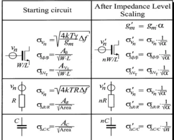
It is a well-known fact that increasing the area of on-chip MOS-transistors improves the matching properties of those transistors [9]. The same also goes for the matching of resistors and capacitors on an IC [10]. This leads us to investigate the effect of increasing the area of a complete circuit in a systematic manner that we call impedance level scaling. The concept of impedance level scaling is fairly simple, yet leads to very useful design considerations. This technique enables a decoupled optimization of the noise and mismatch properties of a circuit independent of other properties such as speed and linearity, thus, simplifying the task of the designer. Starting from a circuit that has been optimized with respect to specifications other than noise and mismatch, one can scale the width of every component of that circuit by a certain factor
α
. This is shown conceptually in Fig. 2.18, where the effect on the component values is also shown.Using the analogy that scaling is similar to putting identical circuits in parallel, as illustrated in Fig. 2.18,
α
=2, it is easy to deduce that the nodevoltages of the scaled circuit are equal to those of the original circuit, provided the circuit is no heavily loaded externally. From this analogy it is also clear that the scaling will not change linearity and speed of the circuit.
A fact that is familiar to many designers is that impedance level scaling will improve the signal to noise ratio of the circuit at the cost of increased power usage. More precisely, scaling the circuit by a factor
α
will decrease the26
rms-value of the noise voltages by a factor α while increasing the power
usage by a factor
α
, meaning there is a direct tradeoff between power usage and noise.A less familiar but important property of impedance level scaling is the effect it has on the mismatch errors of a circuit. Assume the relative change in the value of a certain component changes some circuit parameter ( for example, the offset voltage, or the delay of a delay cell) linearly. This is reasonable as long as mismatch changes the value of a component just slightly. The same relative change of the corresponding component in the scaled circuit will result in the same change of the output parameter, which can again be understood by the scaling analogy depicted in Fig. 2.19 the mismatch of the component value of the scaled circuit will reduce by a factor α , which means the sensitivity of circuit
parameters such as offset and delay errors will be α times less in the scaled
circuit than in the starting circuit, at the cost of increased power usage. For a delay cell, the implication of the impedance level scaling is that increasing the power by a factor
α
yields a stochastic jitter reduction of α (which alsofollows from the jitter analysis in [11]). Also the mismatch of the delay between different cells will improve by a factor α .
27
2.5.3 Analysis of PLL Jitter Caused by Digital
Switching Noise
When combining an analog chip and a digital chip into one mixed-mode design, a particular area of concern is on-chip noise coupling from the digital to the analog circuitries which do not exist in either of the two original chips. In the PLL, the noise generated by digital logic couples through the substrate to an analog circuit will result to large jitter.
The principle of substrate noise coupling is shown in Fig. 2.20. An MOS transistor in the digital section of the chip turns on and discharges a capacitive load generating a brief current pulse in the Vss network. The current pulse is forced through the inductive bonding wire in the Vss path and generates a voltage bounce on Vss. This noise couples through the resistive substrate or through a shared supply network into the analog section of the chip. The amount of noise reaching the analog circuitry is proportional to the inductance and the amplitude of the current spike, but inversely proportional to the impedance of the connecting path. Here it is assumed that noise coupling due to resistance/inductance/capacitance of the on-chip power distribution network can be avoided by proper layout.
Fig 2.20 Noise generated by digital logic couples through the substrate to an analog circuit
28
There are several techniques attempting to reduce the noise injected into the analog circuitry ([12]–[14]). Each of the techniques focuses on one of the three components above(inductance of power supply path, amplitude of current pulse, impedance of connecting path), but often several techniques are combined to achieve a better noise reduction.
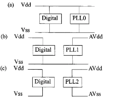
To demonstrate to effect of digital switching noise coupling, the phase-locked loop (PLL) is analyzed for three different power supply schemes. The main mechanisms for noise coupling are identified by comparing different PLLs and varying their bandwidths. The three different power supply distribution schemes in Fig. 2.21 will be studied in the following. In the first case, the digital circuitry and the analog PLL share both Vdd and Vss. Since the switching noise appears on both Vdd and Vss with opposite phase [14], we can expect large noise coupling resulting in large PLL jitter. In the second case, a separate Vdd is used for the analog PLL. Intuitively, we would expect a noise reduction by a factor of two, since half of the noise (the noise coupled through Vdd) is eliminated. With large amount of decoupling capacitance between Vdd and Avdd, the noise would turn into common-mode noise that cannot disturb the PLL, ideally giving no jitter. However, even with ideal capacitive Avdd-Vss coupling, resonance effects where Avdd and Vss resonate at opposite phase will turn the common-mode noise into differential- mode noise [14]. In the third case, the PLL is supplied with both separate Vdd and Vss. With infinite-impedance substrate, this would completely eliminate any noise coupling, but in the case of standard low-resistivity substrate, there is still some coupling. In all three cases, the local Vss is used for substrate contacts. The three power supply schemes are compared in a single chip containing several PLLs and noise generators.
29
The measured jitter at 4-MHz PLL bandwidth is plotted in Fig. 2.22. It shows the RMS jitter as function of the NCk frequency which is the noise generator frequency. In this case, the reference clock was 100 MHz and the division ratio in the PLLs was set to 8, such that the VCOs were running at 800 MHz. For a PLL that shares Vdd and Vss with the digital circuitry, the main jitter source is supply coupling into the VCO. Using separate Vdd and Vss for a PLL causes substrate noise to couple into the loop filter node. The reason for this coupling is parasitic resistances in the epi layer below the MOS transistor used as filter capacitor. A PLL with separate Vdd but sharing Vss with the digital circuitry exhibits far less jitter than the other PLLs. The main cause of jitter in this case is delay variations in the feedback divider that mixes the PLL reference frequency into a low-frequency beat note. If this beat note frequency is lower than the PLL bandwidth, the PLL tracks the beat note. This occurs only when a harmonic of the clock of the noise generating digital circuitry is close to the reference clock driving the PLL.
Fig 2.21 Three power supply schemes under investigation. (a) PLL0: common Vdd and Vss , (b) PLL1: separate analog Vdd , (c) PLL2: separate analog Vdd and Vss
30
The same PLL was also fabricated in a triple-well process. Triple-well technology [15]–[17] is a relatively cheap process enhancement which can be made compatible with standard CMOS processing. It requires an additional implant layer, which is the buried well that extends the standard PMOS tub underneath the NMOS devices. This well breaks the resistive path from the digital noise source into the analog circuits, indicating that it can work as a noise blocking feature when using separate Vdd and Vss networks for the digital and analog circuits. However, there is still finite impedance between the digital and analog sections, since the triple-well has capacitive coupling to the substrate. The cross section in Fig. 2.23 shows a triple-well beneath the analog circuit, but it can also be located under the digital circuitry or both.
31
Test chip was processed in a triple-well technology enabling measurements of three different triple-well conFigurations. For a PLL with separate supplies residing in a triple-well, the jitter in Fig. 2.24(a) was obtained when the NG31 noise generator was active. The jitter of PLL2 in Fig. 2.22 caused by substrate noise coupling into the filter is not present for the triple-well PLL. Furthermore, no noise peaks can be observed at harmonics of the noise clock in Fig. 2.24(a), indicating that the PD/divider noise coupling also is eliminated. A buried well was added to the noise generator NG31s. The jitter of the PLL with a triple-well is shown in Fig. 2.24(b), indicating that the additional benefit in using triple-well beneath both the analog and digital circuits is minor. However, this cannot be a general statement, since the jitter when using triple-well only under PLL2 is very close to the limit of 5–6 ps that was observed without any noise source. When activating NG31s having a triple-well and observing the jitter of a PLL without triple-well, there is still significant coupling causing large jitter at harmonics of the noise clock frequency as shown in Fig. 2.24(c). From this, we conclude that it is more effective to place the PLL in a triple-well than the digital circuitry. The main difference between these two schemes is the effective area of the noise blocking triple-well. The area of the PLL was about 200 x 250um while the area of the noise generator was 1100 x 700m. The area is a direct measure of the capacitive coupling from the substrate to the triple-well. With larger area, the impedance is lower and therefore placing the triple-well under the noise generator is less efficient in blocking the noise.
Fig 2.23 Triple-well processing provides a buried well that breaks the resistive noise coupling path
32
As the measurement results in [18], the jitter performance of three power supply schemes PLLs has been discussed. It is shown that with triple-well process both the noise coupling through the filter and the divider noise at harmonics are eliminated. The importance of keeping the triple-well area small to reduce capacitive coupling was also demonstrated.
Fig 2.24 Jitter induced by NG31 into PLLs having a bandwidth of 4 MHz. Prefix 3W indicates that the block resides in a triple-well
33
Chapter 3
Overview
of
Dynamic
Frequency
Scaling Technique and Proposed Dual
Output Clock Generator with Dynamic
Frequency/Phase Tuning Ability
3.1
Dynamic Frequency Scaling System
In recent years, the power and Energy consumption has become a critical design issue in embedded systems, which have been rapidly and widely spread, especially mobile systems and portable systems. Most embedded devices are operated using batteries so that their working duration is limited. Maintain high performance while extending the battery life is an interesting challenge for system designers. Dynamic Voltage Scaling (DVS) and Dynamic Frequency Scaling (DFS) have established itself as an important technique for saving energy on mobile embedded systems. Dynamic Voltage Scaling and Dynamic Frequency Scaling allow adjusting processor voltage and frequency at runtime to adapt to the workload demand for better energy management. Usually, higher processor voltage and frequency leads to higher system throughput while energy reduction can be obtained using lower voltage and frequency. The dynamic power consumed by a microprocessor is proportional toV f2 , where V refers to the voltage supplied to the processor while f is the frequency at which it is clocked. The expression indicates that the power savings achieved through voltage reduction is quadratic in terms of the voltage change. Similarly a linear energy saving is obtained by reducing the frequency.
34
However, reduction of processor voltage and frequency increases the circuit delay, causing slowdown in the execution. So these two factors cannot be reduced arbitrarily due to primarily two reasons. First, the performance constraints of the concerned applications. Second, the maximum frequency at which the processor can be clocked is limited by the voltage level [19]. Hence, the dynamic selection of the processor voltage and frequency are essentially parts of the same problem. Furthermore the time taken to switch frequencies is typically much less than that taken for changing the voltage level of the processor. Hence, for very short intervals, only the processor frequency may be changed without changing the processor voltage level.
The amount of power or energy savings possible through dynamic voltage and frequency scaling is essentially dependent on the computational requirements of the applications. The mechanism of DFS and DVS is critical to achieve both power saving and performance. According to different system concern, the Dynamic Voltage Frequency Scaling(DVFS) mechanism may be different. In the following sections we will review several dynamic frequency scaling systems. The mechanism of DFS and performance will be discussed.
3.1.1
The Dynamic Frequency Scaling Technique
Most conventional microprocessors are designed using synchronous clock distribution mode. The clock distribution network is designed very carefully to meet the constraints of clock skew. It contributes to the complexity of clock interconnection and the significant increase of microprocessor power. So the designers present asynchronous system which need not clock. But there are so many difficulties in design of the complete asynchronous signals. Globally Asynchronous Locally Synchronous (GALS) [20], which is a compromise between asynchronous systems and synchronous systems, has been focused on. Most current researches on GALS are based on superscalars [21-26], and not been applied to EPIC architecture, because there are much difficulties in its implementation. In [27], it presents multiple clock domains (MCD) EPIC which is done with GALS style. The dynamic frequency scaling technique has been applied, and the simulation results of power saving and performance has been presented.
35
Fig 3.1 shows the conventional EPIC architecture and the MCD partition EPIC architecture. The EPIC microprocessor is partitioned to six clock domains according to the rules 1) this partition can’t change the organization structure of the microprocessor pipelines too much; 2) the domain boundaries are set between the components having a loose coupling with each other. According to the above rules the partition of six domains: a fetching instruction domain (Domain1), a dispatch domain (Domain2), a L2 Cache domain (Domain 3), a load/store domain (Domain4), an integer domain (Domain5), and a floating-point domain (Domain6). The function of Domain1 contains branch prediction, instruction address generation, and I-Cache read. Domain2 accomplishes dispatch of instructions. Domain3 includes L2 Cache read/write operation. L1D-Cache read/write is completed in Domain4. Domain5 completes the load/store operation of integer operands, and execution of arithmetic logic. Domain6 consists of the load/store operation of floating-point operands, and execution of floating-point computing. Each domain has its own local clock. The units within same domain operate in synchronous mode. The queue structures based on the hybrid clock FIFO has been used as the asynchronous communication among different domains.
36
By analyzing processor resource utilization, a correlation is revealed, over an interval of instructions, between the valid entries in the input queue and the desired frequency for the domain. Queue utilization is thus an appropriate metric for dynamically determining the desired domain frequency. The dynamic, adaptive control algorithm of clock domain’s frequency is based on this idea to reduce the power consumption of the clock network. The dynamic, adaptive control attack/decay algorithm [24] is used independently in each back-end domain. When the entries in the domain issue queue is in excess of 10,000-instructions interval, the hardware counts. Using the number and the corresponding number from the previous interval, the algorithm determines whether there is a significant change that threshold is 1.7 percent, in which case the algorithm uses the attack mode: The frequency changes by 7 percent. If no significant change occurs, the algorithm uses the decay mode: It reduces the domain frequency slightly by 0.17 percent.
In order to evaluate it, the basic technology parameter of CACTI 0.8µm is used [28], and scaling down method to implement power consumption evaluation model [29]. Since IMPACT [30] provides a comprehensive infrastructure for modeling and simulation of EPIC microarchitecture feature, the Lsim simulator [30, 31] of the IMPACT compile framework is adopted as the simulation engine. Also, three strategies of frequency voltage control have been simulated to evaluate the dynamic scaling mechanisms:
SVF Strategy: Each of clock domains works on condition that the voltage is same, and frequency is also same, called SVF for simple, which represents same voltage and frequency.
DVF Strategy: Each of clock domains works on condition that the voltage may be different, and frequency may be different, too. The frequency and voltage are not adjusted during the system running. This strategy is called DVF for simple, which denotes different voltage and frequency. The voltage and the frequency of each of domains are set as Table 3.1, according to the architecture characteristic of Itanium 2.
37
DVF+DAA Strategy: Each clock domain works on condition that voltage and frequency maybe different with each other domain. They are also set as Table 2. Furthermore, during the system running, the frequency of each back-end domains is adjusted dynamically and adaptively as the attack/decay algorithm
Fig 3.2 shows the power consumption of the MCD EPIC relative to the basic EPIC processor under three strategies described above. All three MCD EPIC strategies can decrease the microprocessor’s power consumption. Comparing with SVF and DVF, Using DVF+DAA strategy can more effectively decrease the power consumption of the microprocessor, which decreases the power by 40 percent, as a result of using the fine-grained dynamic adaptive frequency adjustment.
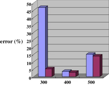
Fig 3.3 shows the impact on the performance that using the different MCDE strategy. The SVF strategy results in a slight degradation, within 1 percent. Comparing with SVF, DVF and DVF+DAA result in more performance degradation owing to clock frequency being decreased. For DVF, the average performance degradation is approximately 6.5 percent. For DVF+DAA, the average performance degradation is about 7.3 percent.
![Fig 2.15 shows the binary weighted digital controlled differential delay cell[5]](https://thumb-ap.123doks.com/thumbv2/9libinfo/8262728.172256/29.892.155.753.127.649/fig-shows-binary-weighted-digital-controlled-differential-delay.webp)