具有超薄非晶矽層之高效能雷射退火複晶矽薄膜電晶體之製作與特性研究
65
0
0
全文
(2) 具有超薄非晶矽層之高效能雷射退火複晶矽薄膜電晶 體之製作與特性研究 The Fabrication and Characterization of High Performance Laser-annealed Polycrystalline Silicon Thin-Film Transistors with an Ultra-Thin Amorphous-Silicon Layer. 研 究 生:楊學人. Student:Hsueh-Jen Yang. 指導教授:張國明 博士. Advisor:Dr. Kow-Ming Chang Dr. Cheng-May Kwei. 國. 立. 電子工程學系 碩. 交. 通. 大. 學. 電子研究所碩士班 士. 論. 文. A Thesis Submitted to Institute of Electronics College of Electrical Engineering and Computer Science National Chiao Tung University In Partial Fulfillment of the Requirements for the Degree of Master In Electronics Engneering June 2004 Hsinchu, Taiwan, Republic of China 中華民國九十三年六月.
(3) 具有超薄非晶矽層之高效能雷射退火複晶矽薄膜電晶 體之製作與特性研究. 研究生:楊學人. 指導教授:張國明 博士 桂正楣 博士. 國立交通大學 電子工程學系 電子研究所碩士班. 摘 要. 本 篇 論 文 中 , 我 們 對 具 有 超 薄 非 晶 矽 層 之 準 分 子 雷 射 退 火 ( excimer laser-annealed)低溫複晶矽薄膜電晶體之特性做了一系列的研究與比較,在不需 要額外的光罩下,藉著覆蓋一層超薄非晶矽層,不僅降低了雷射退火通道之表面 粗糙度也使開/關電流的比值改善了約一個數量級; 另外,也進一步的抑制了扭節 現象的產生。我們發現到超薄非晶矽的最佳覆蓋厚度為 5nm; 研究結果顯示,開 /關電流之比值在汲極電壓為 5V 時可從 4.15 x 10⁴ 提升至 3.45 x10⁵,臨界電壓輕 微的偏移到 2.43V,通道表面粗糙度之方均根(RMS)可改善至 8.52nm,除此之 外,和傳統結構的薄膜電晶體(無超薄非晶矽層)相比,此新穎結構具有較佳的熱 電子應力承受能力。 i.
(4) The Fabrication and Characterization of High Performance Laser-annealed Polycrystalline Silicon Thin-Film Transistors with an Ultra-Thin Amorphous-Silicon Layer. Student: Hsueh-Jen Yang. Advisor: Dr. Kow-Ming Chang Dr. Cheng-May Kwei. Institute of Electronics National Chiao Tung University. Abstract. In this thesis, the characteristics of excimer laser annealed low temperature polycrystalline silicon TFT's with/without an ultra-thin a-Si layer have been investigated and compared. With capping an appropriate ultra-thin a-Si layer, the surface roughness of laser-annealed channel is not only decreased, but also the On/Off current ratio is improved about one order without extra mask step and kink effect is. ii.
(5) further suppressed. We also find that the optimum thickness of capping ultra-thin a-Si layer is about 5-nm. In our study, the On/Off ratio is rose from 4.15 x 10⁴ to 3.45 x 10⁵ for Vds = 5 V, Threshold voltage slightly shift to 2.43 V and RMS surface roughness of channel can be improved to 8.52-nm. And it has better hot-carrier stress endurance than conventional TFTs without an ultra-thin a-Si layer.. iii.
(6) 誌 謝. 謹將這本論文獻給我的父母,楊璨璵先生與賴素香女士。感謝他們從小到大 對我的栽培跟養育,讓我在沒有後顧之憂之下可以順利完成學業研究跟這本論 文,爸爸、媽媽,謝謝!我愛你們! 感謝我的指導教授張國明老師,老師的開明態度跟指導教誨讓我的研究生生 涯受益匪淺,謝謝老師!此外也向交大諸位教導過我的教授們獻上最深的敬意, 因為你們的用心讓我在學術知識上能有所長進。 感謝林俊銘學長在實驗及課業方面給我明確的方向,讓我找到努力的目標。 非常感謝同門師弟葉冠華同學的幫忙與砥礪,讓我在實驗技巧跟許多問題的尋求 解答中,又有了更多的進步。還要感謝雷添福老師實驗室的賴久盟、羅韋翔兩位 同學在實驗過程中的大力協助與指導,以及鄭晃忠老師實驗室的謝振宇同學,沒 有你跟葉冠華在無塵室相陪與談笑,相信從事研究的過程必定是黯然無光的。 謝謝交大奈米中心與國科會 NDL 提供了完整的機台讓我可以順利進行實 驗,也感謝技術員黃月美女士跟林主庫先生的大力幫忙,以及鄭老師實驗室的常 鼎國學長在準分子雷射上的支援,你們都是本論文能夠完成的大功臣。 謝謝一路上陪我走過風風雨雨的同學、學長以及我的好朋友們,因為你們對 我的重情重義、不離不棄,才有今天的我!謝謝各位!. iv.
(7) Contents Chinese Abstract ………………………………………………………………. i English Abstract ………………………………………………………………..ii Acknowledgements …………………………………………………………....iv Contents ………………………………………………………………………...v Table Captions ………………………………………………………………...vii Figure Captions ……………………………………………………………….viii. Chapter 1 Introduction ……………………………………………………….1 1.1 An Overview of Low Temperature Polycrystalline Silicon(LTPS)TFTs 1.2 Recrystallization of Amorphous Si(a-Si)Thin Films 1.2.1 Solid Phase Crystallization 1.2.2 Excimer Laser Annealing Crystallization 1.2.3 Metal-Induced Lateral Crystallization 1.3 Several Novel High Performance Structures for LTPS TFTs 1.4 Reliability Issues in LTPS TFTs 1.5 Motivation 1.6 Thesis Organization Chapter 2. Experimental of Low-Temperature Poly-Si TFTs with an Ultra-Thin a-Si layer …………………………………………….7 2.1 The Fabrication Process flow of Low-temperature Poly-Si TFTs 2.2 Methods of Device Parameter Extraction 2.2.1 Determination of Threshold Voltage 2.2.2 Determination of Subthreshold Swing 2.2.3 Determination of Field Effect Mobility 2.2.4 Determination of On/Off Current Ratio Chapter 3. The Physical Property of Polycrystalline Silicon Thin Films With/Without capping an Ultra-Thin a-Si layer ………………..12. 3.1 The Introduction of SEM and AFM Micorscope Systems 3.1.1 Scanning Electron Microscope System 3.1.2 Atomic Force Microscope System. 3.2 Scanning Electron Microscope Analysis 3.3 Atomic Force Microscope Analysis. v.
(8) Chapter 4. The Electrical Property of Low-Temperature Poly-Si TFTs with an Ultra-Thin a-Si layer ………………….…………………………...16. 4.1 The Characterization of Low-Temperature Poly-Si TFTs with an Ultra-Thin a-Si Layer 4.2 The Reliability of Low-Temperature Poly-Si TFTs with an Ultra-Thin a-Si Layer Chapter 5. Conclusions and Future Work ……………………………………20. 5.1 Conclusions 5.2 Future Work Reference ...............................................................................................................22. vi.
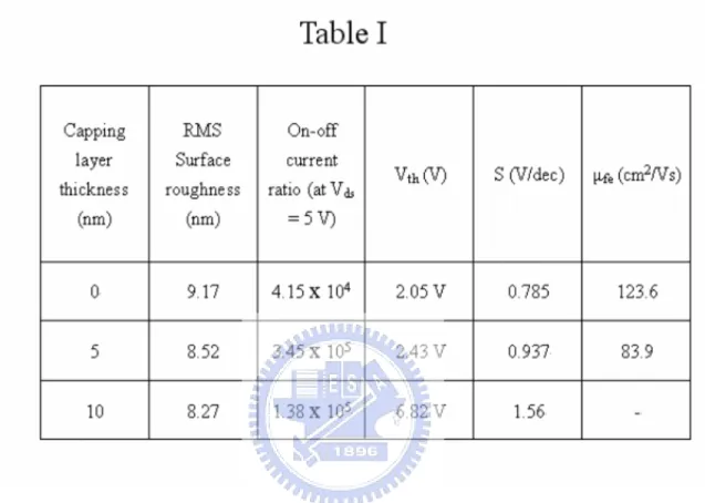
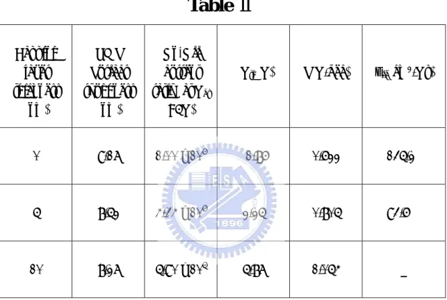
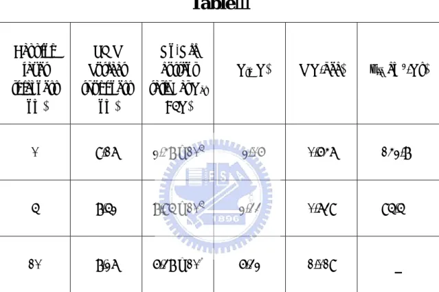
(9) Table Captions Table 1. Major electrical parameters of the ELA Poly-Si TFTs with capping ultra-thin α-Si layer versus with α-Si thicknesses. The On/Off current ratio is measured at Vgs = 5 V. The field-effect mobility (µfe) is measured in the linear region at a Vds of 0.1 V. The threshold voltage is defined at a normalized drain current of (100 nA) x (W/L) at Vgs = 5 V; W/L = 50/10 (µm/µm) Table 2. Major electrical parameters of the ELA Poly-Si TFTs with capping ultra-thin α-Si layer versus with α-Si thicknesses. The On/Off current ratio is measured at Vgs = 5 V. The field-effect mobility (µfe) is measured in the linear region at a Vds of 0.1 V. The threshold voltage is defined at a normalized drain current of (100 nA) x (W/L) at Vgs = 5 V; W/L = 20/20 (µm/µm) Table 3. Major electrical parameters of the ELA Poly-Si TFTs with capping ultra-thin α-Si layer versus with α-Si thicknesses. The On/Off current ratio is measured at Vgs = 5 V. The field-effect mobility (µfe) is measured in the linear region at a Vds of 0.1 V. The threshold voltage is defined at a normalized drain current of (100 nA) x (W/L) at Vgs = 5 V; W/L = 10/10 (µm/µm). vii.
(10) Figure Captions Chapter 2 Figure.2-1 Process flow of fabricating LTPS n-channel poly-Si TFTs Chapter 3 Figure 3-1 Schematic of the primary components of a typical SEM. Figure 3-2 Schematic of the major components of an AFM showing the feedback loop for TappingModeTM operation. Figure.3-3 The SEM image of SPC (solid phase crystallization) poly-Si film Figure.3-4 The SEM image of ELA (excimer laser annealing) poly-Si films Figure.3-5 AFM images of laser annealed poly-Si film. (a)ELA without a-Si layer, (b)ELA with 50 Å a-Si layer, (c)ELA with 100 Å a-Si layer, (d)ELA with 150 Å a-Si layer, (e)ELA with 200Å a-Si layer. The average RMS values were 9.17, 8.52, 8.27 , 7.35 and 6.99nm respectively Chapter4 Figure.4-1 Ids-Vgs transfer characteristics of laser-annealed LTPS TFT’sversus thickness of capping α-Si layer for Vds= 5 V; W/L= 50/10 (µm/µm). Figure.4-2 Ids-Vgs transfer characteristics of laser-annealed LTPS TFT’s versus thickness of capping α-Si layer for Vds= 5 V; W/L= 20/20 (µm/µm).. Figure.4-3 Ids-Vgs transfer characteristics of laser-annealed LTPS TFT’s versus thickness of capping α-Si layer for Vds= 5 V; W/L= 10/10 (µm/µm).. Figure.4-4 Ids-Vgs transfer characteristics of laser-annealed LTPS TFT’s compared with adding 5nm α-Si for Vds=0.1V, 1V and 5V; W/L=50/10 (µm/µm). Figure.4-5 Ids-Vds output characteristics of laser-annealed LTPS TFT’s with/without α-Si layer with versus Vgs; W/L= 50/10 (µm/µm).. viii.
(11) Figure.4-6 The variations of the threshold voltage shifts as a function of the stress time (sec). Figure.4-7 The variations of the maximum transconductance as a function of the stress time (sec).. Figure.4-8 Threshold voltage variation under static hot-carrier stress with various thickness of a-Si. Figure.4-9 The degradation of maximum transconductance under static hot-carrier stress with various thickness of a-Si. Figure 4-10. The variations of the threshold voltage shifts as a function of the stress time (sec).. Figure 4-11 The variations of the maximum transconductance as a function of the stress time (sec). Figure.4-12 Threshold voltage variation under static hot-carrier stress with various thickness of a-Si. Figure.4-13. The degradation of maximum transconductance under static hot-carrier stress with various thickness of a-Si.. ix.
(12) Chapter 1 Introduction 1.1 An Overview of Low Temperature Polycrystalline Silicon(LTPS) TFTs Recently, polycrystalline silicon thin-film transistors(poly-Si TFTs)have been applied to peripheral driving circuits in AMLCDs [1], high density SRAMs [2][3], thermal printer heads [4], linear image sensors [5] and nonvolatile memories [6], photodetector amplifier [7] etc. Most importance of all, poly-Si TFTs are the most promising pixel switching controller in AMLCDs. Traditionally, amorphous silicon thin-film transistors(a-Si:H TFTs) are mainly used for active-matrix addressed LCDs [8]. The a-Si:H TFTs exhibit high OFF-state resistivity which can reduce the leakage current. Unfortunately, they have extremely low field-effect mobility(typically below 1 cm2/V sec).However, poly-Si TFTs have better characteristics than amorphous silicon thin-film transistors, including higher mobility, lower photocurrent and better reliability [9]. Most important advantage of poly-Si TFTs is for their use on the peripheral driving circuit in large-area active matrix liquid crystal displays (AMLCDs). Therefore, we can achieve the goal to system on panel (SOP). But one of the disadvantages of poly-Si TFTs is their high processing temperature which requires the use of an expensive substrate. And the performance of poly-Si TFTs are strongly influenced by grain size, grain boundary and intragranular defects [10]. Thus, the key process for fabricating low temperature process poly-Si TFTs (LTPS TFTs)on glass is the recrystallization technology, such as: solid-phase crystallization (SPC) [11], eximer laser annealing (ELA) [12]-[14], metal-induced lateral crystallization (MILC) [15]-[17], rapid thermal annealing (RTA) [18], and microwave crystallization [19]. Besides, various device architectures which are 1.
(13) different from the conventional self-aligned source/drain structure have also been adopted to enhance TFT performance and reliability. In the following sections, more detail information about the key processes and those useful device architectures, such as offset gate [20]-[21], gate-overlapped LDD [22]-[24], lightly doped drain (LDD) [25]-[26] are introduced to enhance LTPS TFTs’ parameters such as on/off current ratio, subthreshold swing and field-effect mobility[27].. 1.2 Recrystallization of Amorphous Si(a-Si)Thin Films The performance of LTPS TFTs is strongly influenced by grain boundary and intragranular defects. In order to increase the grain size of poly-Si films as possible as lower temperature, several methods have been proposed. In the following, three kinds of low temperature crystallization methods are roughly reviewed.. 1.2.1. Solid Phase Crystallization Amorphous silicon thin films deposited by low-pressure chemical vapor. deposition(LPCVD)below 600℃ annealed in furnace at 600℃ several hours(~24 h). The films will be converted into polycrystalline form, and the grain sizes obtained by this method(SPC)is more larger and smoother morphology than as-deposited poly-Si films. However, due to the low deposition temperature used, long crystallization duration is necessary, and large defect density exists in crystallized poly-Si.. 1.2.2. Excimer Laser Annealing Crystallization Laser crystallization is a much faster process than others. Especially, excimer. laser crystallization is by far most widely used method now [12]-[14]. Because excimer laser is the strong absorption of UV light in silicon, most of the laser energy is deposited close to the surface of the a-Si films. The laser process heats the a-Si 2.
(14) films to the melting point in a very short duration(several nanoseconds)without damaging the glass substrate, and the silicon films will melt and recrystallize. Because ELA process has the highest annealing temperature among the other methods, we can obtain the higher quality poly-Si films.. 1.2.3. Metal-Induced Lateral Crystallization A certain metal, for example, Al [28], Cu [29], Ag [30], or Ni [31], are. deposited on a-Si. By annealing in furnace they will transform to metal silicide. Considering the metal-Si eutetic temperature, an a-Si thin tilm can be crystallized below 500℃. Consequently, the metal-induced crystallized (MIC)process is lower than SPC annealing temperature to get low temperature process. However, in spite of low crystallization temperature, metal contamination is a serious problem in MIC poly-Si. To improve its property, metal-induced lateral crystallization(MILC)process has demonstrated that high performance LTPS TFTs can be fabricated using Ni-MILC.. 1.3 Several Novel High Performance Structures for LTPS TFTs Generally speaking, poly-Si TFTs have two different structures : top-gate coplanar structure and bottom-gate structure. The top-gate TFTs have mainly used in AMLCD applications because their self-aligned source/drain regions provide low parasitic capacitances and is suitable for device scaling down. On the other hand, thought bottom-gate TFTs have better interface and higher plasma hydrogenation rate than top-gate TFTs, They have lower current and need extra process steps for backside exposure. The dominant leakage current mechanism in poly-Si TFTs is the field emission via grain boundary traps by a high electric field near the drain [32]. Thus, reducing the 3.
(15) electric field near the drain junction is required. Today, many device structures have been proposed to improve poly-Si TFTs performance. For example, Offset Gated Structure(Offset TFTs)[20]-[21] and Lightly Doped Drain Structure(LDD TFTs) [25]-[26] are two kinds of new TFT structures. Both of them were proposed due to suppress the off-state leakage current, but the on-state current is lowered at the same time. Besides, an extra mask in LDD structures and misalignment in Offset TFTs are two major problems. Thus, how to reduce off-state current without degrade ton-state current too much is a trade-off. Finally, the reliability of new structures is quite concerned because all TFTs are worked for long-term.. 1.4 Reliability Issues in LTPS TFTs The stability of device characteristics under long-term operation is indispensable for circuit applications. As a result, the reliability of LTPS TFTs must be taken into consideration when they are applied to advanced circuitry such as data-driver in AMLCDs or driving elements in AMOLEDs. The special processes used in the fabrication of LTPS TFTs and nature properties of crystallized poly-Si make the reliability issues in LTPS TFTs different from those in the conventional MOSFETs. The gate oxide used in LTPS TFTs is generally deposited at low temperature by CVD method. Consequently, it always exhibits poorer physical and electrical quality, such as low density, high gate leakage current, and low breakdown field, compared to high-temperature thermal grown oxide used in MOSFETs. Crystallized poly-Si is generally full of weak strain Si-Si bonds and dangling bonds. Besides, the hydrogenation process also creates a large amount of weak Si-H bonds in poly-Si. These weak bonds can easily be broken during devices operation,. 4.
(16) which will result in the variation of devices characteristics [33]. The surface roughness of poly-Si resulting from laser crystallization will enhance the local electrical field near the interface between gate oxide and channel poly-Si, which will also degrade the reliability of TFT under high gate bias operation. The hot carrier effects which originate from high electric field near the drain junction have been widely investigated in MOSFETs. Meanwhile, it is also another important reliability issue in LTPS TFTs. Generally, introducing electric-field-relief TFT structures, such as LDD, offset drain, and gate-overlapped LDD, can reduce the hot carrier degration.. 1.5 Motivation Excimer laser crystallized polycrystalline silicon (poly-Si) films are promising for active layer of high performance poly-Si thin film transistors (TFT’s), which are utilized as driving or switching devices in active-matrix liquid-crystal-displays (AMLCD’s), However, the surface of the laser crystallized poly-Si films is rather rough due to the explosive protrusion of grain boundaries during the grain growth [34], which results in the increase of the roughness at the poly-Si/SiO2 interface. It is also reported that the field-effect mobility of TFT devices is affected by the roughness of the gate insulator. Considerable efforts have been paid to improve the surface roughness of poly-Si because the electrical characteristics of TFT’s are seriously affected by the interface roughness of the gate insulator. In this thesis, we introduce an ultra-thin a-Si layer on the poly-Si channel layer. And we will show the AFM images of the improvement channel layer. In order to investigate the effect of the surface roughness on the device performance, we have studied the electrical characteristics. Besides, the reliability of the device will be discussed. 5.
(17) 1.6 Thesis Organization In chapter 1, a brief overview of LTPS TFT technology and related applications were introduced. In chapter 2, the fabrication process flow of the new TFT device, experimental recipes, and device parameter extraction methods will be described. In chapter 3, we will show the physical property of the poly-Si film, includes AFM and SEM images of the interface roughness and the poly-Si grain size. In chapter 4, we will show the electrical property of the new TFT device, includes transfer characterization, output characterization and the reliability issue. Finally, conclusions and future work as well as suggestion for further research are given in chapter 5.. 6.
(18) Chapter 2 Experimental of Low-Temperature Poly-Si TFTs with an Ultra-thin a-Si layer. 2.1 The Fabrication Process flow of Low-temperature Poly-Si TFTs The poly-Si TFTs were fabricated on 4-inch-diameter p-type silicon wafer. Fig.2-1 shows the process flow of unhydrogenation poly-Si TFTs. The 100nm undoped amorphous silicon (a-Si) films were initially deposited on 500nm thermally oxidized silicon (100) wafers by low-pressure chemical vapor deposition (LPCVD) system with silane (SiH4) gas at 550。C. The deposition pressure was 100 mtorr and the silane flow rate was 40 sccm. Afterward semi-gussiam shaped KrF excimer laser crystallization was carried out with wavelength of 248 nm in 10-4 Torr at 320mJ/cm2 energy density and 400。C substrate heating [35]-[36]. Then, an ultra-thin a-Si layer was deposited on the recrystallized poly-Si layer. After defining the device active areas, a 50 nm-thick TEOS oxide film was deposited at 350。C to serve as the gate dielectric by PECVD. Then, a 300 nm thick poly-Si was deposited by LPCVD at 600。C with SiH4 for the gate electrode. Gate areas were patterned and the regions of source, drain, and gate electrode were doped by a self-aligned 5x10¹⁵ ions/cm2 phosphorus implantation with a He-diluted PH3 gas , at 50 KeV of acceleration voltage. The dopant were activated at 600。C in N2 ambient for 24 hr. Next, a 500nm TEOS oxide was deposited by PECVD at 350。C as a passivation layer, and contact lithography was carried out. After opening contact holes, a 500 nm Al was deposited by evaporation and the metal layer was patterned. Finally, the samples were sintered at 400。C for 30min in N2 gas ambient.. The detailed fabrication process flow is listed as follows. 7.
(19) 1.. (100) orientation Si wafer. 2.. Initial cleaning. 3.. Thermal wet oxidation at 1050。C to grow 5000Å thermal SiO2 in furnace. 4.. 1000 Å a-Si was deposited by LPCVD at 550。C in SiH4 gas. 5.. KrF excimer laser crystallization was carried out in 10-4 Torr at 320 mJ/cm2 energy density and 400。C substrate heating. 6.. 50 Å,100 Å,150 Å,200 Å a-Si were deposited by LPCVD at 550。C in SiH4 gas. 7.. Mask#1 : define active regions (poly-Si dry etch by Poly-RIE system). 8.. RCA cleaning. 。 9. 500 Å gate dielectric deposition by PECVD at 350 C. 10.. 3000 Å poly-Si was deposited by LPCVD at 620。C in SiH4 gas. 11.. Mask#2: Define gate regions (poly-Si dry etch by Poly-RIE system). 12.. Ion implantation: P31 , 50KeV, 5x10¹⁵ ions/cm2. 13.. Dopant activation in N2 ambient at 600。C for 24hrs in furnace. 14. 5000 Å TEOS oxide was deposited by PECVD as passivation layer 15.. Mask#3: Open contact holes. 16.. 5000 Å Al thermal evaporation. 17. Mask#4: Al pattern defined 18.. Etching Al and removing photoresist. 19.. Al sintering at 400。C in N2 ambient for 30 min. 2.2 Methods of Device Parameter Extraction. 8.
(20) Many methods have been proposed to extract the characteristic parameter of poly-Si TFT. In this section, the methods of parameter extraction used in this research are described.. 2.2.1 Determination of Threshold Voltage (Vth) The threshold voltage Vth is an important MOSFET parameter required for the channel length-width and series resistance measurement. However, Vth is a voltage that is not uniquely defined.Various definition exist and the reason for this can be found in the ID-VGS curves. One of the most common threshold voltage measurement technique is the linear extrapolation method with the drain current measured as a function of gate voltage at a low drain voltage of typically 50-100 mV to ensure operation in the linear MOSFET region [37]. But the drain current is not zero below threshold and approaches zero only asymptotically. Hence the ID verus VGS curve is extrapolated to ID=0, and the threshold voltage is determined from the extrapolated or intercept gate voltage VGSi by Vth = VGSi − VDS 2. (Eq. 2.1). Equation (2.1) is strictly only valid for negligible series resistance. Fortunately series resistance is usually negligible at the low drain currents where threshold voltage measurement are made. The ID-VGS curve deviate from a straight line at gate voltage below Vth due to subthreshold currents and above Vth due to series resistance and mobility degradation effects. It is common practice to find the point of maximum slope on the ID-VGS curve by maximum in the transconductace fit a straight line to the ID-VGS curve at that point and extrapolate to ID=0.. 2.2.2 Determination of Subthreshold Swing. Subthreshold swing S.S (V/dec) is a typical parameter to describe the control 9.
(21) ability of gate toward channel. That is the turn on/off speed of a device. It is defined as the amount of gate voltage requires to increase/decrease drain current by one order of magnitude. The subthreshold swing should be independent of drain voltage and gate voltage. However, in reality, the subthreshold swing might increase with drain voltage due to short channel effect such as charge sharing, avalanche multiplication, and punchthrough effect. The subthreshold swing is also related to gate voltage due to undesirable and inevitable factors such as serial resistance and interface state. In my thesis, the subthreshold swing is defined as one-third of the gate voltage required to decrease the threshold current by three orders of magnitude. The threshold current is specified to be the drain current when the gate voltage is equal to threshold voltage. 2.2.3 Determination of Field Effect Mobility ( µ FE ). Usually, µ FE is extracted from the maximum value of transconductance (gm) at low drain bias (VDS=1V). The drain current in linear region (VDS< VGS-Vth) can be approximated as the following equation:. I DS = µ FE Cox (. W 1 2 )[(VGS − Vth )VDS − VDS ] L 2. (Eq. 2.2). where W and L are width and length, respectively. Cox is the gate oxide capacitance. Thus, gm is given by. gm =. ∂I DS W = µ FE Cox ( )VDS ∂VGS L. (Eq. 2.3). L g m (max) VDS →0 CoxWVDS. (Eq. 2.4). Therefore,. µ FE =. 10.
(22) 2.2.4 Determination of On/Off Current Ratio. On/Off current ratio is one of the most important parameters of poly-Si TFTs Since a good performance means not only large On current but also small Off (leakage) current. The leakage current mechanism in poly-Si TFTs is not like it in MOSFET. In MOSFET, the channel is composed of single crystalline and the leakage current is due to the tunneling of minority carrier from drain region to accumulation layer located in channel layer region. However, in poly-Si TFTs, the channel is composed of poly crystalline. A large amount of trap densities in grain structure attribute a lot of defect state in energy band gap to enhance the tunneling effect. Therefore, the leakage current due to the tunneling effect is much larger in poly-Si TFTs than in single crystalline devices. When the voltage drops between gate voltage and drain voltage increase, the band gap width decrease and the tunneling effect becomes much more severe. Normally we can find this effect in typical poly-Si TFT ID-VG characteristics where the magnitude of leakage current will reach a minimum and then increase as the gate voltage decrease/increase for n/p-channel TFTs. There are a lot of ways to specify the On and Off current. In my thesis, take n-channel poly-Si TFTs for examples, the On current and Off current is defined as the drain current when gate voltage equal to 15V and drain voltage is 1 V(linear operation mode). The Off current is specified as the minimum leakage current in linear operation mode for usual cases. I ON Maximum current of I DS − VGS plot at VDS = 1V = I OFF Minimum current of I DS − VGS plot at VDS = 1V. 11. (Eq. 2.5).
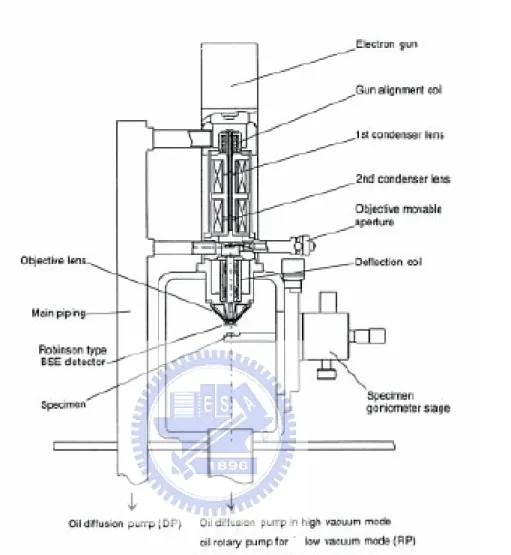
(23) Chapter 3 The Physical Property of Polycrystalline Silicon Thin Films with/without Capping an Ultra-Thin a-Si Layer. 3.1 The Introduction of SEM and AFM Micorscope Systems. 3.1.1. Scanning Electron Microscope (SEM) System. The operation of the SEM consists of applying a voltage between a conductive sample and filament, resulting in electron emission from the filament to the sample. This occurs in a vacuum environment ranging from 10-4 to 10-10 Torr. The electrons are guided to the sample by a series of electromagnetic lenses in the electron column. A schematic of a typical SEM is shown in Figure. 3-1. The resolution and depth of field of the image are determined by the beam current and the final spot size, which are adjusted with one or more condenser lenses and the final, probe-forming objective lenses. The lenses are also used to shape the beam to minimize the effects of spherical aberration, chromatic aberration, diffraction, and astigmatism. The electrons interact with the sample within a few nanometers to several microns of the surface, depending on beam parameters and sample type. Electrons are emitted from the sample primarily as either backscattered electrons or secondary electrons. Secondary electrons are the most common signal used for investigations of surface morphology. They are produced as a result of interactions between the beam electrons and weakly bound electrons in the conduction band of the sample. Some energy from the beam electrons is transferred to the conduction band electrons in the sample, providing enough energy for their escape from the sample surface as secondary electrons. Secondary electrons are low energy electrons (<50eV), so only those formed within the first few nanometers of the sample surface have enough 12.
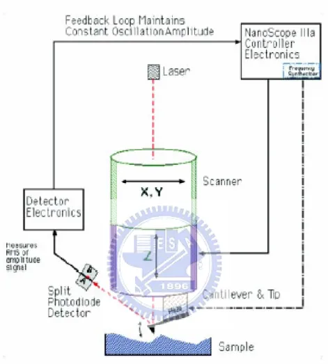
(24) energy to escape and be detected. High energy beam electrons which are scattered back out of the sample (backscattered electrons) can also form secondary electrons when they leave the surface. Since these electrons travel farther into the sample than the secondary electrons, they can emerge from the sample at a much larger distance away from the impact of the incident beam which makes their spatial distribution larger. Once these electrons escape from the sample surface, they are typically detected by an Everhart-Thornley scintillator-photomultiplier detector. The SEM image formed is the result of the intensity of the secondary electron emission from the sample at each x,y data point during the rastering of the electron beam across the surface.. 3.1.2. Atomic Force Microscope (AFM) System. AFM consists of scanning a sharp tip on the end of a flexible cantilever across a sample surface while maintaining a small, constant force. An integrated silicon tip and cantilever can be seen in Figure. 3-2. The tips typically have an end radius of 2nm to 20nm, depending on tip type. The scanning motion is conducted by a piezoelectric tube scanner which scans the tip in a raster pattern with respect to the sample (or scans to the sample with respect to the tip). The tip-sample interaction is monitored by reflecting a laser off the back of the cantilever into a split photodiode detector. By detecting the difference in the photodetector output voltages, changes in the cantilever deflection or oscillation amplitude are determined. The two most commonly used modes of operation are contact mode AFM and TappingMode AFM, which are conducted in air or liquid environments. Contact mode AFM consists of scanning the probe across a sample surface while monitoring the change in cantilever deflection with the split photodiode detector. A feedback loop maintains a constant cantilever deflection by vertically moving the scanner to 13.
(25) maintain a constant photodetector difference signal. The distance the scanner moves vertically at each x,y data point is stored by the computer to form the topographic image of the sample surface. This feedback loop maintains a constant force during imaging, which typically ranges between 0.1 to 100nN. TappingMode AFM consists of oscillating the cantilever at its resonance frequency (typically ~300kHz) and lightly “tapping” on the surface during scanning. The laser deflection method is used to detect the root-mean-square (RMS) amplitude of cantilever oscillation. A feedback loop maintains a constant oscillation amplitude by moving the scanner vertically at every x,y data point. Recording this movement forms the topographical image. The advantage of TappingMode with respect to contact mode is that it eliminates the lateral, shear forces present in contact mode. This enables TappingMode to image soft, fragile, and adhesive surfaces without damaging them, which can be a drawback of contact mode AFM.. 3.2 Scanning Electron Microscope (SEM) Analysis For device applications, the physical properties of the poly-Si thin films are of major interest. The primary concerns are the grain size, quality of grains and the grain size distribution, and these properties will strongly influence the electrical characteristics of poly-Si. It is believed that electrical properties of the TFTs can be improved if the grain size can be enhanced and the number of grain boundaries can be minimized in the channel [38]-[39]. Fig. 3-3, and Fig. 3-4 show the grain size of SPC (solid phase crystallization) poly-Si and ELA (excimer laser annealing) poly-Si films. In the case of SPC, a-Si films were crystallized at 600。C for 24hr. In the other case of ELA, KrF excimer laser crystallization was carried out in 10-4 Torr at 320 mJ/cm2 energy density and 400。C substrate heating. The SEM images clearly show that the ELA poly-Si film has larger grain size than that of SPC poly-Si film. However, the 14.
(26) surface of the laser crystallized poly-Si films is rather rough due to the explosive protrusion of grain boundaries during the grain growth, which results in the increase of the roughness at the poly-Si/SiO2 interface [38]. It is also reported that the field-effect mobility of TFT devices is affected by the roughness of the gate insulator [39]. Considerable efforts have been paid to improve the surface roughness of poly-Si because the electrical characteristics of TFT’s are seriously affected by the interface roughness of the gate insulator [40]-[42].. 3.3. Atomic Force Microscope (AFM) Analysis According to section 3.2, we know that the surface roughness of poly-Si is an. important issue to the electrical characteristics and reliability of TFT’s [43]. In order to decrease the surface roughness of poly-Si, many efforts have been introduced [44]-[46]. In this thesis, we introduce an ultra-thin a-Si layer which deposited onto the poly-Si layer. Different thickness of a-Si layer were used to optimize the best physical and electrical performance. Furthermore, in order to investigate the surface morphology of the interface between oxide film and poly-Si, we use atomic force microscope (AFM) to measure the surface roughness of poly-Si films which were recrystallized by KrF excimer laser with and without an ultra-thin a-Si layer. Fig. 3-5(a), (b), (c), (d) and (e) show that the average rms values of roughness were 9.17, 8.52, 8.27, 7.35 and 6.99 nm respectively. It can be saw that the pure ELA poly-Si. film has the maximum average rms value of roughness. When we increase the thickness of a-Si nano layer, the average rms value of roughness was decreased obviously. Besides, the average rms value will approach to saturation as the thickness of a-Si is up to 200 Å . Consequently, we successfully decrease the surface roughness by introducing an ultra-thin a-Si layer and the thickness of a-Si layers is lower than 200 Å . 15.
(27) Chapter 4 The Electrical Property of Low-Temperature Poly-Si TFTs with an Ultra-Thin a-Si Layer. In this chapter, we will discuss the device performance and reliability of poly-Si TFTs with/without an ultra-thin a-Si layer. We measured the thickness of the films by n&k analyzer, and the I-V characteristics of poly-Si TFTs by HP4156 semiconductor parameter analyzer.. 4.1 The Characterization of Low-Temperature Poly-Si TFTs with an Ultra-Thin a-Si Layer Ids-Vgs transfer characteristics of laser-annealed LTPS TFT’s with/without a-Si layer are shown in Figure 4-1. It is clearly that the optimum condition is ELA with 5-nm a-Si layer. Obviously, Both turn-on currents (measured at Vgs= 20 V) and off-state leakage currents (measured at Vgs= -8 V) are reduced with a-Si layer thickness increasing. The main reason for lower off-state leakage current of the ELA TFT capping with ultra-thin a-Si layer is that the drain electric field is greatly reduced due to high-resistively a-Si layer near the drain side [47]. In the other hand, higher grain boundary trap density of a-Si layer also suppressed turn-on current. For the optimum condition, Ioff, min is suppressed about one order but turn-on current almost close to conventional ELA TFT. We considered that the degree of surface roughness improved by capping with 5-nm a-Si layer will effectively raise turn-on current even though capping with a-Si layer will decrease turn-on current. Therefore, turn-on current finally is not reduced obviously in this optimum condition. However, turn-on 16.
(28) current was significantly reduced with the thickness of capped a-Si layer increasing. It was inferred that the reduction of the turn-on current due to higher grain boundary trap density of a-Si layer became dominate. At Vds = 5 V, the on-off current ratios of the ELA TFT and the ELA TFT with 5-nm α-Si layer are 4.15 x 10⁴ and 3.45 x 10⁵, respectively. The on-off current ratio is defined as that ratio of the maximum turn-on current to the minimum off-state current. The detail parameters are shown in Table 1. In Figure 4-2 and Figure 4-3, we also show the same trend with different sizes of TFT devices. All the detail parameters are shown in Table 2 and Table 3, respectively. Fig. 4-4 shows the transfer characteristics of optimum condition compared with conventional laser-annealed TFT for Vds=0.1V, 1Vand 5V. In Figure 4-5, Ids-Vds output characteristics of laser-annealed LTPS TFT’s with/without ultra-thin a-Si layer are shown. Obviously, less kink effect can be observed in ELA TFT with ultra-thin a-Si layer to further confirm that the drain electric field can be effectively reduced as a-Si layer thickness increasing for both Vgs= 5 V and 10 V. It is because that the kink current in TFT devices is basically due to the avalanche or impact ionization in the device and is strongly influenced by grain boundary traps [48]. The grain boundary traps can prevent the channel carriers from gaining higher energy, and therefore the impact ionization probability can be reduced as the grain boundary trap density is increased [48]. It is well known that the grain boundary trap density of a-Si layer is usually higher than that of Poly-Si layer. Therefore, laser-annealed Poly-Si channel capping with ultra-thin a-Si layer will effectively reduce the drain electric field and further suppress kink effect generation. Above all, we can see that laser-annealed LTPS TFT’s with appropriate a-Si layer thickness will not only improve the surface roughness of laser annealed poly-Si. 17.
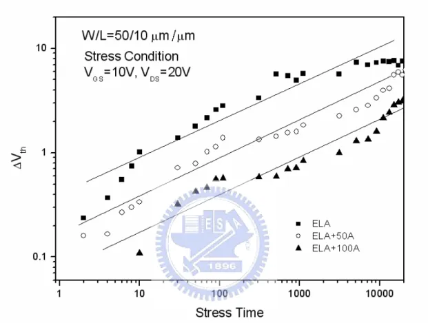
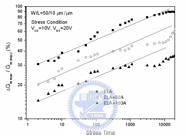
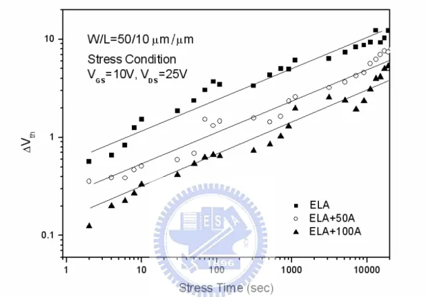
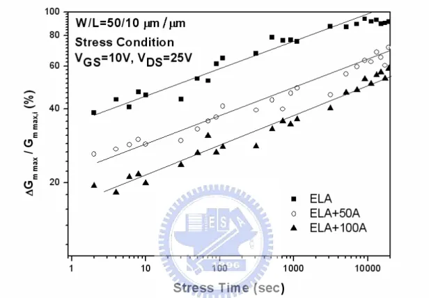
(29) and on-off current ratio, but also effectively suppress kink effect for suitable condition. The optimization of a-Si layer thickness is 5-nm in our study.. 4.2 The Reliability of Low-Temperature Poly-Si TFTs with an Ultra-Thin a-Si Layer Fig. 4-6 , Fig. 4-7, Fig. 4-10 and Fig. 4-11 show the threshold voltage variations and the degradation of the maximum transconductance under static hot-carrier stress which is defined as the TFT being kept at a high electric field in the drain junction. Notably, the dc stress conditions are (1)VGS =10V and VDS =20V (2) VGS =10V and VDS =25V. The △Vth is defined as Vth,s –Vth, i where Vth, i denotes the initial Vth and Vth, s represents the Vth for etch stress time. Moreover, the degradation of the Gm max is defined as △Gm max /Gm max, i ,where △Gm max = △Gm max, s - △Gm max, i,. Gm max, i denotes the initial Gm max and Gm max, s represents the Gm max for each stress. time. The △Vth and △Gm max /Gm max, i are measured at 1.0 V for etch stress time. Both △Vth and △Gm show the same power-time dependence. Therefore, acceptor-like trap states are generated at the gate oxide / channel interface and silicon grain boundaries [49]. Because some of the holes will be injecting into the gate oxide at high drain bias, the other holes will migrate to the minimum of potential within the channel. Therefore, some of holes are trapped in the gate oxide / channel interface near drain and the other are accumulated / trapped near the channel / bottom oxide interface near source. The acceptor-like trap states at gate oxide / channel interface are the dominating factor for △Vth and △Gm. Fig. 4-8, Fig. 4-9, Fig. 4-12 and Fig. 4-13 also show the threshold voltage variations and the degradation of the maximum transconductance under static hot-carrier stress with different thickness of a-Si layer. When we increase the thickness of a-Si, we improve the interface roughness and decreace the trap states between gate oxide and channel. So one can see that △Vth 18.
(30) and △Gm degrade slightly as the thickness of a-Si increased.. 19.
(31) Chapter 5 Conclusions and Future Work. 5.1 Conclusions In this thesis, we have utilized ultra-thin amorphous silicon layers deposited by low pressure chemical vapor deposition (LPCVD) to solve the main problem of the explosive protrusion of grain boundaries during the grain growth for using laser annealing. Furthermore, it also improved the reliability, the characteristics of conventional excimer laser annealed Poly-Si TFT’s and suppressed kink effect without extra mask step. For our optimum condition which α-Si layer thickness is 5-nm, The on-off current ratio is improved from 4.15 x 10⁴ to 3.45 x 10⁵ at Vds = 5 V, Threshold voltage is 2.43 V and the RMS surface roughness can improve to 8.52-nm. Therefore, the use of ultra-thin a-Si layers for fabricated TFTs exhibit significantly superior electrical characteristics and reliability to the conventional Poly-Si TFTs. Hence, the proposed high performance Poly-Si TFTs are promising for the application of integrated circuits on LCD panel.. 5.2 Future Work We have proposed a low-temperature Poly-Si TFTs with an ultra-thin a-Si layer to improve conventional low-temperature Poly-Si TFTs performance. However, in order to further improve device electrical characteristics and apply to glass substrates, there are still some works worthy of being investigated. We could use various CVD systems such as PECVD, ECR-CVD to deposited a-Si layers and we can use RTA process instead of furnace thermal annealing to further confirm the optimal condition. Moreover, the dynamic stress is closer to real operation conditios than static stress [50], we could study the degradation mechanism. 20.
(32) by analyzing the evolution of device parameters including transconductance, threshold voltage, and sub-threshold slope.. 21.
(33) Reference. [1] T.Serilawa, S.shirai, A. Okamoto, and S. Suyama, “Low-temperature fabrication of high-mobility Poly-Si TFTs for large-area LCD’s,” IEEE Trans. Electron Dev., vol. 36, no. 9, pp. 1929,1989. [2] S. Ikeda et al., “A polysilicon transistor technology for large capacity SRAMs,” IEDM Tech. Dig., pp. 469, 1990. [3] F. Hayashi and M. Kitakata, “A high performance polysilicon TFT using RTA and plasma hydrogenation applicable to highly stable SRAMs of 16 Mbit and beyond, “ VLSI Technology, 1992. Digest of Technical Papers. 1992 Symposium on, 1992, p36-37 [4] Y. Hayashi et al., “A thermal printer head with CMOS thin-film transistor and heating elements integrated on a chip,” ESSCC Digest, pp. 266, 1988. [5] S. Morozumi et al., “Completely integrated contact-type linear image sensor,” IEEE Trans. Electron Devices., vol. 21, no. 8, p. 1546, 1985 [6] H. C. Lin et al., “Deposition and Device application of in situ Boron doped Polycrystalline SiGe Films Grown at Low Temperature,” J. Appl Phys., vol. 42, no. 9, pp. 835-837, 1993. [7] N. Yamauchi, Y. Inaba, and M. Okamura, “An integrated photodetector amplifer using α − Si p-i-n photodiodes and poly-Si thin-film transistors,” IEEE Photonic Tec. Lett.,vol. 5, no. 3, p.319, 1993. [8] H. C. Tuan, “Amorphous silicon thin film and its applications to large-area elements,” Master. Rec. Soc. Ump. Proc., vol. 33, p.247, 1984. [9] J. R. Ayres and N. D. Young, “Hot carrier effects in devices and circuits formed from poly-Si,” IEEE proc. Circuits Devices Syst., vol. 131, no. 1, p.38, 1994. [10] Tien-Fu Chen, Ching-Fa Yeh, and Jen-Chung Lou, “Investigation of Grain Boundary 22.
(34) Control in the Drain Junction on Laser-Crystalized Poly-Si Thin Film Transistors,” IEEE Electron Device Lett., vol. 24, no. 7, 2003. [11] A. Nakamura, F. Emoto, E. Fujii, and A, Tamamoto “A High-Reliability, Low-Operation-Voltage Monolithic Active-Matrix LCD by Using Advanced Solid-Phase growth Technique,” IEDM Tech. P.847, 1990. [12] G. K. Giust and T. W. Sigmon, “Low-Temperature Polysilicon Thin-Film Transistors Fabricated from Laser-Processed Sputtered-Silicon Films,” IEEE Electron Device Lett., vol. 19, pp. 343-344, Sept. 1998. [13] N. Kubo, N. Kusumoto, T. Inushima, and S. Yamazaki, “Characterization of polycrystalline-Si thin-film transistors fabricated by excimer laser annealing method,” IEEE Trans. Electron Devices, vol. 40, pp. 1876-1879, Oct. 1994. [14] G. K. Giust and T. W. Sigmon, “High-Performance Laser-Processed Polysilicon Thin-Film Transistor,” IEEE Electron Device Lett., vol. 20, no. 2, pp. 77-79, Feb. 1999. [15] Won Kyu Kwak, Bong Rae Cho, Soo Young Yoon, Seong Jin Park, And Jin Jang, “A High Performance Thin-Film Transistor Using a Low Temperature Poly-Si by Silicide Mediated Crystallization,” IEEE Electron Device Lett., vol. 21, no. 3 March 2000. [16] Seok-Woon Lee, Tae-Hyung Ihn, and Seung-Ki Joo, “Fabrication of High-Mobility P-Channel Poly-Si Thin Film Transistors by Self-Aligned Metal-Induced Lateral Crystallization,” IEEE Electron Device Lett., vol. 17, no. 8 Aug. 1996. [17] Zhiguo Meng, Mingxiang Wang, and Man Wong, Member, IEEE, “High Performance Low Temperature Metal-Induced Unilaterally Crystallized polycrystalline. Silicon. Thin. Film. transistors. for. System-on-Panel. Application,” IEEE Trans. Electron Devices, vol. 47, no. 2, Feb. 2000. 23.
(35) [18] Eric Campo, Emmanuel Scheid, Danielle Bielle-Daspet, and Jean-Paul Guillemet, “Influence of Rapid Thermal and Low Temperature Processing on the Electrical Properties of Polysilicon Thin Film Transistors,” IEEE Trans. On Semi. Manufacturing, vol. 8, no.3 Aug. 1995. [19] Yong Woo Choi, Jeong O Lee, Tae Woong Jang, and Byung Tae Ahn, “Thin-Film Transistors Fabricated with Poly-Si Films Crystallized at Low Temperature by Microwave Annealing,” IEEE Electron Device Lett., vol. 20, no. 1, pp. 2-4, Jan. 1999. [20] K. Tanaka, H. Arai, and S. Kohda, “Characteristics of offset-structure polycrystalline-silicon thin-film transistors,” IEEE Electron Device Lett., vol. 9, pp. 23-25, 1988. [21] B. H. Min, C. M. Park, and M. K. Han, “A novel offset gated polysilicon thin film transistor without an additional offset mask,” IEEE Electron Device Lett., vol. 16, pp. 161-163, 1995. [22] Yasuyoshi Mishima and Yoshiki Ebiko, “Improved lifetime of poly-Si TFTs with a self-aligned gate-overlapped LDD structure,” IEEE Trans. Electron Devices, vol. 49, pp. 981-985, 2002. [23] M. Hatano, H. Akimoto, and T. Sakai, “A novel self-aligned gate-overlapped LDD poly-Si TFT with high reliability and performance,” in IEDM Tech. Dig., 1997, pp. 523-526. [24] Kwon-Young Choi, Jong-Wook Lee, and Min-Koo Han, “Gate-overlapped lightly doped drain poly-Si thin film transistors for large area-AMLCD,” IEEE Trans. Electron Devices, vol. 45, pp. 1272-1279, 1998. [25] Byung-Hyuk Min and Jerzy Kanicki, “Electrical characteristics of new LDD poly-Si TFT structure tolerant to process misalignment,” IEEE Electron Device Lett., vol. 20, pp. 335-337, 1999. 24.
(36) [26] Shengdong Zhang, Ruqi Han, and Mansun J. Chan, “A novel self-aligned bottom gate poly-Si TFT with in-situ LDD,” IEEE Electron Devices Lett., vol. 22, pp. 393-395, 2001. [27] I. W. Wu, T. Y. Huang, W. B. Jackson, A. G. Lewis, and A. Chiang, “Passivation kinetics of two types of defects in polysilicon TFT by plasma hydrogenation,” IEEE Electron Devices Lett., vol. 12, no.4, p. 181, 1991. [28] G. Radnoczi, A. Robertsson, H. T. G. Hentzell, S. F. Gong, and M. A. Hasan, “Al induced crystallization in of a-Si,” J. Appl. Phys., vol. 69, pp. 6394-6399, 1991. [29] S. W. Russel, Jian Li, and J. W. Mayer, “In situ observation of fractal growth during a-Si crystallization in a Cu3Si matrix,” J. Appl. Phys., vol. 70, pp. 5153-5155, 1991. [30] Bo Bian, Jian Yie, Boquan Li, and Ziqin Wu, “Fractal formation in a-Si:H/Ag/a-Si:H films after annealing,” J.Appl.Phys., vol. 73, pp. 7402-7406, 1993. [31] Yunosuke Kawazu, Hiroshi Kudo, Seinosuke Onari, and Toshihiro Arai, “Low-temperature crystallization of hydrogenated amorphous silicon induced by nickel silicide formation,” Jpn. J. Appl. Phys. Part1, vol. 29, pp. 2698-2704, 1990. [32] K. R. Olasupo, M. K. Hatalis, “Leakage current mechanism in sub-micron polysilicon thin-film transistors,” in IEDM Tech. Dig., 1993, pp. 385-388 [33] I-Wei Wu, Warren. B. Jackson, Tiao-Yuan Huang, Alan G. Lewis, and Anne Chiang, “Mechanism of device degradation in n- and p-channel polysilicon TFT’s by electrical stressing,” IEEE Electron Device Lett., vol. 11, pp. 167-170, 1990. [34] Jae-Hong Jeon, Juhn-Suk Yoo, Cheol-Min Park, Hong-Seok Choi, and Min-Koo Han, “ A Novel Method for a Smooth Interface at Poly-SiOx/SiO2 by Employing 25.
(37) Selective Etching,” IEEE Electron Device Letters, vol. 21, no.4, p. 152, 2000. [35] C. W. Lin, M. Z. yang, C.C. Yeh, L. J. Cheng, T. Y. Huang, H. C. Cheng, H. C. Lin, T. S. Chao, and C. Y. Chang, “Effect of plasma treatment, substrate types and crystallization methods on performance and reliability of low temperature polisilicon TFTs,” in IEDM Tech. Dig., 1999, pp.305-308. [36] C. H. tseng, C. W. Lin, T. K. Chang, H. C. Cheng, and A. Chin, “Effects ofexcimer laser dopant activation on the low temperature polysilicon thin-film transistors with lightly doped drains,” Electrochem. Solid-State Lett., vol. 4, no. 11, pp. G94-97, 2001. [37] Dieter K. Schroder, “Semiconductor Material and Device Characterization,” Wiley-INTERSCIENCE, 1998. [38] H. Wang, S. Jagar, S. Lam, and M. Chan, ”High frequency performance of large-grain polysilicon-on-insulator MOSFETs, ” IEEE Trans. Electron Devices, vol. 48, pp. 1480-1482. JUL. 2001. [39] S. Jagar, M. Chan, M. C. Poon, H. Wang, M. Qin, P. K. Ko, Y. Wang, “Single grain thin-film-transistor (TFT) with SOI CMOS performance formed by metal-induced-lateral crystallization,” International Electron Device Meeting Technical Digest, pp. 293-296, 1999. [40] Jae-Hong Jeon, Juhn-Suk Yoo, Cheol-Min Park, Hong-Seok Choi, and Min-Koo Han, “A Novel Method for a Smooth Interface at Poly-SiOx/SiO2 by Employing Selective Etching,” IEEE Electron Device Letts., VOL. 21, NO. 4, APRIL 2000. [41] K. Takechi, H. Uchida, and S. Kaneko, “Mobility improvement mechanism in a-Si : H TFT’s with smooth a-Si : H/SiNx interface,” in Proc. Mat. Res. Soc. Symp., 1992, vol. 258, p. 955. [42] K. Takechi, H. Uchida, and S. Kaneko, “Mobility improvement mechanism in a-Si:H TFT’s with smooth a-Si:H/SiN interface,” in Proc. Materials Research 26.
(38) Soc. Symp., vol. 258, 1992, p. 955. [43] R. Moazzami and C. Hu, “A high-quality stacked thermal/LPCVD gate oxide technology for ULSI,” IEEE Electron Device Lett., vol. 14, p. 72, 1993 [44] C. Y. Chang et al., “Fabrication of thin film transistors by chemical mechanical polished polycrystalline silicon films,” IEEE Electron Device Lett., vol. 17, p. 100, 1996. [45] J. Y. Lee., C. H. Han, and C. K. Kim, “ECR plasma oxidation effects on performance and stability of polysilicon thin-film transistors,” in IEDM Tech. Dig., 1994, p.523. [46] R. Moazzami and C. Hu, “A high-quality stacked thermal/LPCVD gate oxide technology for ULSI,” IEEE Electron Device Lett., vol. 14, Feb. 1993. [47] A. C. Ipri, “Method of forming an improved gate dielectric for a MOSFET on an insulating substrate,” U.S. Patent 4 758 529, Hopewell Township, NJ, July 1988. [48] Kow Ming Chang, Yuan Hung Chung, Gin Ming Lin, Jian Hong Lin and Chi Gun Deng, “ A novel high-performance poly-silicon thin film transistor with a self-aligned thicker sub-gate oxide near the drain/source regions,” IEEE Electron Device Letters, vol. 22, no. 10, p. 472, 2001. [49] Anish Kumar K.P., Johnny K. O. Sin, Cuong T. Nguyen, and Ping K. Ko, “Kink-Free Polycrystalline Silicon Double-Gate Elevated-Channel Thin-Film Transistors,” IEEE Trans. Electron Devices, vol. 45, no. 12, p. 2514. 1998 [50] Kow Ming Chang, Yuan Hung Chung, and Gin Ming Lin,”Anomalous Variation of OFF State Leakage Current in Poly-Si TFT under Static Stress,” IEEE Electron Device Letters, Vol. 23, No. 5, pp. 255-257, May 2002. 27.
(39) Table 1. Major electrical parameters of the ELA Poly-Si TFTs with capping ultra-thin α-Si layer versus with α-Si thicknesses. The On/Off current ratio is measured at Vgs = 5 V. The field-effect mobility (µfe) is measured in the linear region at a Vds of 0.1 V. The threshold voltage is defined at a normalized drain current of (100 nA) x (W/L) at Vgs = 5 V; W/L = 50/10 (µm/µm).
(40) Table Ⅱ Capping layer thickness (nm). RMS Surfacr roughness (nm). On-Off current ratio (at Vds =5V). 0. 9.17. 5. 10. Vth(V). S(V/dec). µfe(cm2/Vs). 1.00 x 10⁶. 1.86. 0.622. 135.2. 8.52. 4.34 x 10⁶. 2.25. 0.805. 93.6. 8.27. 5.90 x 10⁵. 5.87. 1.054. _. Table 2. Major electrical parameters of the ELA Poly-Si TFTs with capping ultra-thin α-Si layer versus with α-Si thicknesses. The On/Off current ratio is measured at Vgs = 5 V. The field-effect mobility (µfe) is measured in the linear region at a Vds of 0.1 V. The threshold voltage is defined at a normalized drain current of (100 nA) x (W/L) at Vgs = 5 V; W/L = 20/20 (µm/µm).
(41) TableⅢ Capping layer thickness (nm). RMS Surfacr roughness (nm). On-Off current ratio (at Vds =5V). 0. 9.17. 5. 10. Vth(V). S(V/dec). µfe(cm2/Vs). 2.48 x 10⁵. 2.06. 0.647. 142.8. 8.52. 8.95 x 10⁵. 2.33. 0.739. 95.5. 8.27. 6.38 x 10⁴. 6.32. 1.019. _. Table 3. Major electrical parameters of the ELA Poly-Si TFTs with capping ultra-thin α-Si layer versus with α-Si thicknesses. The On/Off current ratio is measured at Vgs = 5 V. The field-effect mobility (µfe) is measured in the linear region at a Vds of 0.1 V. The threshold voltage is defined at a normalized drain current of (100 nA) x (W/L) at Vgs = 5 V; W/L = 10/10 (µm/µm).
(42) (a) Thermal oxidation. (b) LPCVD a-Si, recrystallization, capped a-Si and define active layer.
(43) (c) Deposit SiO2 dielectric by PECVD and define poly-Si gate. (d) Ion implantation (self-align) and dopant activation.
(44) (e) Deposit PECVD TEOS oxide as passivation layer. (f) Define contact holes and Al electrode Fig.2-1 Process flow of fabricating LTP n-channel poly-Si TFTs.
(45) Fig 3-1. Schematic of the primary components of a typical SEM..
(46) Fig 3-2. Schematic of the major components of an AFM showing the feedback loop for TappingModeTM operation..
(47) Fig.3-3 The SEM image of SPC (solid phase crystallization) poly-Si film.
(48) Fig.3-4 The SEM image of ELA (excimer laser annealing) poly-Si films.
(49) (a)ELA without a-Si layer. (b)ELA with 50 Å a-Si layer.
(50) (c)ELA with 100 Å a-Si layer. (d)ELA with 150 Å a-Si layer.
(51) (e)ELA with 200Å a-Si layer. Fig.3-5 AFM images of laser annealed poly-Si film. (a)ELA without a-Si layer, (b)ELA with 50 Å a-Si layer, (c)ELA with 100 Å a-Si layer, (d)ELA with 150 Å a-Si layer, (e)ELA with 200Å a-Si layer. The average RMS values were 9.17, 8.52, 8.27 , 7.35and 6.99nm respectively.
(52) Fig.4-1 Ids-Vgs transfer characteristics of laser-annealed LTPS TFT’s versus thickness of capping α-Si layer for Vds= 5 V; W/L= 50/10 (µm/µm)..
(53) Fig.4-2 Ids-Vgs transfer characteristics of laser-annealed LTPS TFT’s versus thickness of capping α-Si layer for Vds= 5 V; W/L= 20/20 (µm/µm)..
(54) Fig.4-3 Ids-Vgs transfer characteristics of laser-annealed LTPS TFT’s versus thickness of capping α-Si layer for Vds= 5 V; W/L= 10/10 (µm/µm)..
(55) Fig.4-4 Ids-Vgs transfer characteristics of laser-annealed LTPS TFT’s compared with adding 5nm α-Si for Vds=0.1V, 1V and 5V; W/L=50/10 (µm/µm)..
(56) Fig.4-5 Ids-Vds output characteristics of laser-annealed LTPS TFT’s with/without α-Si layer with versus Vgs; W/L= 50/10 (µm/µm)..
(57) Fig 4-6 The variations of the threshold voltage shifts as a function of the stress time (sec)..
(58) Fig 4-7 The variations of the maximum transconductance as a function of the stress time (sec)..
(59) Fig.4-8 Threshold voltage variation under static hot-carrier stress with various thickness of a-Si..
(60) Fig.4-9 The degradation of maximum transconductance under static hot-carrier stress with various thickness of a-Si..
(61) Fig 4-10 The variations of the threshold voltage shifts as a function of the stress time (sec)..
(62) Fig 4-11 The variations of the maximum transconductance as a function of the stress time (sec)..
(63) Fig.4-12 Threshold voltage variation under static hot-carrier stress with various thickness of a-Si..
(64) Fig.4-13 The degradation of maximum transconductance under static hot-carrier stress with various thickness of a-Si..
(65) 簡歷. 姓. 名:楊學人. 性. 別:男. 出生日期:民國 69 年 04 月 05 日 出 生 地:台灣省台北市 住. 址:台北市文山區萬利街 30 巷 39 弄 16 號 4 樓. 學. 歷:台北市立成功高級中學. (民國 84 年 9 月~87 年 6 月). 國立中興大學物理學系. (民國 87 年 9 月~91 年 6 月). 國立交通大學電子工程所碩士班. (民國 91 年 9 月~93 年 6 月). 碩士論文:具有超薄非晶矽層之高效能雷射退火複晶矽薄膜電晶體之製作與特性 研究 The Fabrication and Characterization of High Performance Laser-annealed Polycrystalline Silicon Thin-Film Transistors with an Ultra-Thin Amorphous-Silicon Layer..
(66)
數據
+6
相關文件
• 後段工程是從由矽晶圓切割成一個一個的晶片 入手,進行裝片、固定、接合連接、注模成 形、引出接腳、按印檢查等工序,完成作為元
在1980年代,非晶矽是唯一商業化的薄膜型太 陽能電池材料。非晶矽的優點在於對於可見光
雙極性接面電晶體(bipolar junction transistor, BJT) 場效電晶體(field effect transistor, FET).
“Polysilicon Thin Film Transistors Fabricated at 100℃ on a Flexible Plastic Substrate,” IEEE Electron Device Meeting, p. “Polysilicon Thin Film Transistors
―Low-Temperature Polycrystalline Silicon Thin Film Transistor Nonvolatile Memory Using Ni Nanocrystals as Charge-Trapping Centers Fabricated by Hydrogen Plasma
Keywords:Micro-array Biological Probes, E-Beam Evaporator, Active RFID, Laser Annealing, Bioelectric Impedance, Thin Film Transistor
• 雙極性電晶體 (bipolar junction transistor , BJ T) 依結構區分,有 npn 型及 pnp 型兩種. Base
X-ray diffractograms of liquid crystalline polymers.... TGA results of polymers
