國
立
交
通
大
學
顯示科技研究所
碩
碩
碩
碩
士
士
士
士
論
論
論
論
文
文
文
文
具氧化物之電阻式隨機存取記憶體
Oxide-Based Resistive Random Access Memory
研 究 生:鄭又瑋
指導教授:李柏璁 教授
中
中
中
中
華
華
華
華
民
民
民
民
國
國
國
國
九
九
九
九
十
十
十
十
九
九
九
九
年
年
年
年
七
七
七
七
月
月
月
月
i
具氧化物之電阻式隨機存取記憶體
學生:鄭又瑋
指導教授:李柏璁 博士
國立交通大學顯示科技研究所碩士班
摘
要
本篇論文中,我們使用磁控濺鍍的二氧化矽薄膜來實現無機的電阻式記憶體, 以及探討後退火製程對元件電性的影響。結果發現經過後退火處理的元件可以展 現較好的電性,由其在可靠性量測得到大幅的改善。此外,我們也分析元件在高 導電態的載子傳輸行為,探討了記憶體元件在不同退火條件下的載子傳輸機制。 為了朝向更低成本以及大量生產的目標發展,我們製作了兩種結構的有機電
阻式記憶體元件,分別是 AlOx/Alq3雙層和 Alq3/MoO3/Alq3三層結構。實驗結果
顯示:雙層結構的 AlOx/Alq3之介面缺陷態主導元件的記憶體特性,使得元件在電
性上展現近 6 個數量級的高開關電流比;三層結構的記憶體特性源自具奈米結構
的 MoO3與 Alq3的能帶差所形成的載子捕捉中心,並且該元件展現了 4 個數量
Oxide-Based Resistive Random Access Memory
student:You-Wei Cheng
Advisors:Dr. Po-Tsung Lee
Display Institute,
National Chiao Tung University
Abstract
In this thesis, we demonstrate inorganic resistive random access memory (RRAM) using sputtered SiO2 thin films, and investigate the influences of electrical characteristics
of the devices with various post-annealing conditions. The results show that devices with RTA treatment can exhibit better electrical characteristics, especially in the significant improvement of endurance. We also analyze carrier transport behaviors in the high conductance state of devices and propose carrier transport mechanisms under different RTA treatments.
In addition, we fabricate two different structures of organic RRAM: AlOx/Alq3
bi-layer and Alq3/MoO3/Alq3 tri-layer structures. It is found that interface defects at the
AlOx/Alq3 interface dominate the resistive switching of organic RRAM using the bi-layer
structure, and the high ON/OFF current ratio near 106 is obtained; the switching behavior of organic RRAM using the tri-layer structure originate from carrier confinement barriers produced by the difference of energy bands between the nano-structure MoO3 and Alq3
layers, and this devices exhibit a high ON/OFF current ratio about 104 and provide many write-read-erase-read cycles.
iii
Acknowledgements
首先我要感謝我的父母,因為你們做為我的後盾,我才得以升學念書進而取得碩 士班學位,你們的辛苦我都知道,謝謝你們。也謝謝其他家人,你們的關心帶給我溫 暖及勇氣。特別要感謝祐祐表姊,在北部的求學過程蒙受妳很多的照顧,謝謝。 再來要感謝我的指導老師李柏璁教授,感謝老師兩年來的指導與教誨。在學術研 究上老師循循善誘並且教導我們正確的知識觀念和邏輯,因此我才可以順利的完成這 份論文。更謝謝老師的支持和推薦,讓我們可以出國參加學術研討會。也要感謝博班 學長張資岳,提供我研究的方向和協助我解決實驗上的問題。另外要感謝明峰學長、 家揚學長、光揚學長幫我修改論文初稿;謝謝學弟書維和學妹文齡在我們趕實驗時幫 我去洗 wafer 和做 RTA。還要特別感謝兩個人,一個是胖胖蔡宜恆,你是我見過最隨 性無私的人之一,感謝你在 sputter 上的支援;另外一個是光揚,雖然你說話很機車, 但是你滿實在的。謝謝 PTLee lab.贊文學長、小博士品佐,學弟雋威、紹平、立勛 和 401 室其他同學,小瓜呆、趴趴、光廷、治翔、俊傑等,因為有你們,使我在研究 生的生活增添了色彩,謝謝你們。 另外,我的好朋友介瑋、孟詰、映佑、胖卓…等,謝謝你們一路走來的關心,有 你們我才能樂觀堅持。最後要感謝的是我的女朋友可欣北鼻,是妳在我身邊分享我的 喜悅,分擔我的憂愁,持續地、不間斷地一直鼓勵我照顧我支持我忍受我幫助我欺負 我,謝謝妳,有妳真好。 2010/07/05 于新竹 國立交通大學 交映樓 401 室Content
Abstract (in Chinese) ……….……… i
Abstract (in English) ……….…... ii
Acknowledgements ……… iii
Content ……… iv
List of Tables ……… vi
List of Figures ……… vii
Chapter 1
Introduction
1 1.1 Introduction ... 11.2 Oxide-based Resistive Random Access Memory ... 2
1.2.1 Inorganic RRAM ... 2
1.2.2 Organic RRAM ... 5
1.3 Models of Carrier Transport ... 10
1.3.1. Fowler-Nordheim Tunneling ... 10
1.3.2. Foole-Frenkel Emission ... 11
1.3.3. Schottky Emission ... 12
1.3.4. Space Charge Limited Current (SCLC) ... 13
1.4 Motivation ... 14
Chapter 2
Inorganic RRAM Using Sputtered SiO
2Films
15 2.1 Fabrication of the RRAM with Ag/SiO2/p+-Si Structure... 152.2 Electrical Characteristics of Ag/SiO2/p+-Si RRAM Devices ... 16
2.3 Mechanism and Discussion ... 25
2.3.1. Mechanism ... 25
2.3.2. Curve Fitting of I-V Currents ... 28
v
Chapter 3
Organic RRAM Using Metal Oxide
383.1 Introduction ... 38
3.2 Fabrication of the Organic RRAM ... 39
3.2.1. AlOx/Alq3 Bi-layer Structure ... 39
3.2.2. Alq3/MoO3/Alq3 Tri-layer Structure ... 40
3.3 Organic RRAM with AlOx/Alq3 Bi-layer Structure ... 42
3.3.1. Electrical Characteristics ... 42
3.3.2. Mechanism ... 44
3.3.3. Summary ... 50
3.4 Organic RRAM with Alq3/MoO3/Alq3 Tri-layer ... 51
3.4.1. Introduction ... 51
3.4.2. Electrical Characteristics ... 52
3.4.3. Mechanism ... 56
3.4.4. Electrode Effect on Re-writing characteristic ... 62
3.4.5. Summary ... 65
Chapter 4
Conclusion and Future Work
67 4.1 Conclusion ... 674.2 Future Work ... 68
Reference
71List of Tables
Table 2.1 The parameters of fabrication process of Ag/SiO2/p+-Si devices…...……...16
Table 2.2 The parameters of electrical measurements of Ag/SiO2/p+-Si devices……..19
Table 2.3 The measurements of retention time of Ag/SiO2/p+-Si structure with different
RTA conditions………...……...21 Table 2.4 The measurements of endurance of Ag/SiO2/p+-Si structure with different
RTA conditions………..…24 Table 2.5 Fitting results of the high conductance states of Ag/SiO2/p+-Si structure with
different RTA conditions………..……….31 Table 2.6 The performances of Ag/SiO2/p+-Si structure under different RTA
conditions………..………….37 Table 3.1 Th e p ar am e t e rs o f fa b ri ca t i o n p r o c es s o f Al / Al Ox/ Al q3/ n+- S i
device……….…40 Table 3.2 The parameters of fabrication process of Al/Alq3/MoO3/Alq3/p+-Si
vii
List of Figures
Fig 1.1 Schematic structure of a conventional flash memory………….……….……...2 Fig 1.2 Electrical characteristics of Pt/Ti/Al2O3/Pt structure.………..4
Fig 1.3 Electrical characteristics of Cu/ZrO2:Cu/Pt memory devices.…………..……5
Fig 1.4 Current-voltage characteristics of AIDCN/Al nano-cluster/AIDCN sandwich structure.………7
Fig 1.5 AFM image of Al nano-cluster.……….………....7
Fig 1.6 Current-voltage characteristics of Al/PCm: Au nano-particles/Al sandwich structure.………..……..8 Fig 1.7 Cross session TFM image of Au nano-particles in PCm matrix.…………..…9
Fig 1.8 Depiction of F-N tunneling………..11
Fig 1.9 Depiction of P-F emission………12
Fig 1.10 Depiction of Schottky emission………...……….13
Fig 2.1 Schematic diagram of Ag/SiO2/p+-Si structure with different RTA conditions
on SiO2 thin film: (a) as-deposited, (b) RTA 600oC, (c) RTA 800oC.….…...16
Fig 2.2 The current-voltage characteristics of Ag/SiO2/p+-Si structure with different
RTA conditions on SiO2 thin film: (a) as-deposited, (b) RTA 600oC, (c) RTA
800oC……….…...19
Fig 2.3 The retention times of Ag/SiO2/p+-Si structure with different RTA conditions
on SiO2 thin film: (a) as-deposited, (b) RTA 600oC, (c) RTA 800oC…...…...21
Fig 2.4 The write-read-erase-read cycles of Ag/SiO2/p+-Si structure with different
RTA conditions on SiO2 thin films: (a) as-deposited, (b) RTA 600oC, (c) RTA
800oC.……….………..….24
Fig 2.5 Raman spectrum of SiO2/p+-Si structure with as-deposited, RTA 600oC, and
Fig 2.6 The c-AFM images of SiO2/p+-Si structure: (a) 2-D, and (b) 3-D…….……...27
Fig 2.7 The current-voltage measurements of as-deposited, RTA 600oC, RTA 800oC treated samples under various temperatures from 298K to 398K.…………...28 Fig 2.8 Curve fitting of the I-V curves of the high conductance state of Al/SiO2/p+-Si
structure in a log-log plot: (a) as-deposited, (b) RTA 600oC, (c) RTA
800oC.……….………..30
Fig 2.9
Fig 2.10
Path of carrier transport for as-deposited and RTA 600oC treated samples: (a) path1: conductive filaments, and (b) path2: SCLC……….……...…..32 Depiction of Mechanisms of carrier transport in the high conductance state for
RTA 800oC treated sample.……….………...…..33
Fig 2.11 C-V characteristics of Ag/SiO2/p+-Si/Au structure of the as-deposited, RTA
600oC, and RTA 800oC treatments.………..………....34
Fig 2.12 Fitting of the I-V curve of the low conductance state of Ag/SiO2/p+-Si structure
under different RTA conditions in a log (I) - E1/2 plot: (a) as-deposited, (b)
RTA 600oC, and (c) RTA 800oC……….……….…...36
Fig 3.1 (a) Schematic diagram of Al/AlOx/Alq3/n+-Si structure.………..……...39
(b) Structural formula of Alq3……….39
Fig 3.2 Schematic diagram of (a) Alq3/ MoO3 nano-clusters/Alq3 structure. (b)
Standard devices of Alq3 single layer.……….………...41
Fig 3.3 Typical I-V curves of the Al/AlOx/Alq3/n+-S structure……….…...43
Fig 3.4 Retention measurement of the reported Al/AlOx/Alq3/n+-Si structure…...…..44
Fig 3.5 Schematic diagram of the (a) Ag/Alq3/n+-Si structure, and (b) Ag/AlOx /n+-Si
structure……….……….…...…45 Fig 3.6 Current-voltage (I-V) curves of the Ag/AlOx/n+-Si structure……….….…….46
ix
Fig 3.8 Schematic band diagram of the Al/AlOx/Alq3/n+-Si structure……..…..……..48
Fig 3.9 Depictions of proposed mechanisms for the Al/AlOx/Alq3/n+-Si structure…..49
Fig 3.10 Fitting of the I-V curve of the high conductance state of Al/AlOx/Alq3/n+-Si
structure in a log (I/V)-V1/2 plot..………...…………..50 Fig 3.11 Schematic band diagram of the Al/Alq3/MoO3/Alq3/p+-Si structure……...….52
Fig 3.12 I-V characteristics of an organic RRAM with an Al/Alq3/ MoO3 nano-clusters
(5nm)/Alq3/p+-Si structure………...………..…………...54
Fig 3.13 Fig 3.14 Fig 3.15 Fig 3.16 Fig 3.17 Fig 3.18 Fig 3.19 Fig 3.20 Fig 3.21 Fig 3.22
Retention time measurement of the organic RRAM.……….…..55 Write-read-erase-read cycles measurement for Al/Alq3/ MoO3 nano-clusters
(5nm)/Alq3/p+-Si structure………..………..56
(a) The depiction of the writing process for the organic RRAM…….………57 (b) The depiction of the erasing process for the organic RRAM……….……57 I-V characteristics of the standard device with an Al/Alq3 (100nm)/p+-Si
structure……….………59 I-V characteristics of the sample with the Al/Alq3/ MoO3 nano-clusters
(3nm)/Alq3/p+-Si structure……….………...………59
I-V characteristics of the sample with the Al/Alq3/ MoO3 nano-clusters
(8nm)/Alq3/p+-Si structure………..………..………60
Surface morphology of the 3 nm-thick MoO3 layer deposited on the Alq3
/p+-Si………...………..….………61
Surface morphology of the 5 nm-thick MoO3 layer deposited on the Alq3
/p+-Si………..………..….….………61
Al (2p) XPS curve of the Al/Alq3 interface of the Al/Alq3/MoO3/Alq3/p+-Si
structure………..………..…….…………62 I-V characteristics of an organic RRAM with an Ag/Alq3/ MoO3 nano-clusters
Fig 3.23 Fig 3.24 Fig 4.1 Fig 4.2 Fig 4.3 Fig 4.4
(5nm)/Alq3/p+-Si structure…..………..………64
Write-read-erase-read cycles measurement for Ag/Alq3/ MoO3 nano-clusters
(5nm)/Alq3/p+-Si structure.……….…….…….……64
More than 35 cycles of write-read-erase-read measurement for Ag/Alq3/ MoO3
nano-clusters (5nm)/Alq3/p+-Si structure……….………….……65
Schematic diagram of Ag/Alq3/ MoO3 nano-clusters (5nm) /Alq3/Au/PET
structure……….………69 Typical I-V curves of the Ag/Alq3/ MoO3 nano-clusters (5nm)/Alq3/Au/PET
structure before bending………….………..………69 Typical I-V curves of the Ag/Alq3/ MoO3 nano-clusters (5nm)/Alq3/Au/PET
structure after bending ten times………..……….……70 Surface morphology of the PET substrate..……….….……70
1
Chapter 1.
Introduction
1.1.
Introduction
Nonvolatile storage device of flash memory is one of the most famous memories
in recent years due to the advantages of fast read access time, robust, portable, and
high density of data storage. However, a tremendous demand for large amount of data
and information storage is necessary, because we are in the information explosion and
a rapid development of computer and electronic devices of times. Therefore, the
nonvolatile memory (NVM) for next generation has attracts extensive attention due to
the conventional flash memory approaching its scaling limits. The memories with
capacity of three-dimension (3-D) stacking have most potential for high density data
storage.
Fig. 1.1 depicts the schematic structure of a conventional flash memory, and this
transistor-based structure is complicated and unsuitable for 3-D stacking. Moreover,
when the tunneling oxide thickness is below 10nm, the charge stored in the floating
Fig. 1.1: Schematic structure of a conventional flash memory
The potential
next-ferroelectrical random access memory, magnetic random access memory, and
resistive random access memory has been widely
random access memory is more
fabrication process, fast read access time,
capability of 3-D stacking.
1.2.
Resistive Random Access Memory (RRAM)
1.2.1.
Inorganic RRAM
The change of resistivity in
by T.W. Hickmoot [1]. After that, various
TiO2 [7], Nb2O5 [8], and ZrO
simple compositions which are easy
Fig. 1.1: Schematic structure of a conventional flash memory
-generation memory such as phase-changed memory,
random access memory, magnetic random access memory, and
resistive random access memory has been widely studied. Among those
random access memory is more promising due to the simple structure
process, fast read access time, low operation voltage, and especially the
D stacking.
Resistive Random Access Memory (RRAM)
Inorganic RRAM
The change of resistivity in insulator has been discovered in the early 1962 years
. After that, various insulators such as Al2O3 [2
, and ZrO2 [9-11]have been extensively investigated due to the
le compositions which are easy to control during the fabrication process. Fig. 1.1: Schematic structure of a conventional flash memory
changed memory,
random access memory, magnetic random access memory, and
. Among those, resistive
structure, simple
low operation voltage, and especially the
has been discovered in the early 1962 years
[2-4], NiO [5-6],
have been extensively investigated due to the
3
However, the mechanism of resistive switching property is not clearly understood
until now. So far, the formation and fracture of filamentary paths are most acceptable
to elucidate the resistivity switching occurring in oxide films.
It has been proposed that filamentary paths consist of oxygen vacancies and
oxygen-related defects in nonstoichiometry oxide [2], and penetrated metal particles
[3], metal ions in solid electrolyte [12]. For example, Tseung-Yuen Tseng et al
propose a structure of Pt/Ti/Al2O3/Pt/Ti/SiO2/Si, where resistive switching is
dominated by filamentary paths formation in Al2O3 layer. Because of the strong
oxygen-gettering ability of Ti, the oxygen ions will escape from Al2O3 and getter with
Ti under a suitable applied voltage, called forming voltage. Therefore, the oxygen
vacancies and oxygen-related defects are generated and modified to form conducting
paths in Al2O3 thin film.
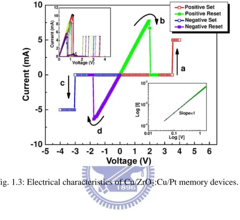
Fig. 1.2 displays the typical electrical characteristics of Pt/Ti/Al2O3/Pt structure,
and its mechanism is dominated by filamentary paths. Compliance current is set in the
writing process during the electrical measurement. Because the joule heat of a large
current in erasing process (where arrow points in Fig. 1.2) may burn the conducting
filamentary paths, the devise will be changed from high conductance state (ON state)
to low conductance state (OFF state). In their work, they also discover the forming
600oC post-annealing treatment do not need a forming p
of Ti into Al2O3 thin film which connect two electrodes.
Fig. 1.2: Electrical
In the other hand, some researches of metal doped oxide as the
in MIM structure of RRAM have been manifested. For example, W. Guan et al
propose an RRAM with Cu doped ZrO
the electrical characteristics
ON-state. This ohmic conductio
filamentary paths, which originate
such as Cu doped MoO3
annealing treatment do not need a forming process due to the
thin film which connect two electrodes.
Electrical characteristics of Pt/Ti/Al2O3/Pt structure.
In the other hand, some researches of metal doped oxide as the
f RRAM have been manifested. For example, W. Guan et al
propose an RRAM with Cu doped ZrO2. As shown in a linear-linear plot of Fig. 1.
characteristics exhibit a linear relation between current and voltage in
his ohmic conduction is ascribed to the formation of conducti
amentary paths, which originate from Cu ions diffusion. Moreover, other studies
[13] and Cu doped SiO2 [14] are also proposed due to the
rocess due to the penetration
structure.
In the other hand, some researches of metal doped oxide as the insulator layer
f RRAM have been manifested. For example, W. Guan et al
linear plot of Fig. 1.3,
exhibit a linear relation between current and voltage in
n is ascribed to the formation of conducting
from Cu ions diffusion. Moreover, other studies
5
great diffusion ability of Cu ions in oxide films. This kind RRAM with metal doped
oxide can provide better memory performance.
Fig. 1.3: Electrical characteristics of Cu/ZrO2:Cu/Pt memory devices.
1.2.2.
Organic RRAM
In recent years, there has been an increasing interest in organic electronic devices
such as OTFT [15], OPV [16], OLED [17]…etc, owing to low cost, simple fabrication
process, massive production, low power driving, and flexibility. Therefore, many
researchers in nonvolatile memory field have widely developed RRAM devices using
organic materials, for instances, nano-structure based devices, donor-acceptor type,
and charge-transfer complexes based devices have been proposed to demonstrate the
The nano-structure based devices can be classified according to the organic
materials. One is organic small molecular materials blended with core-shell
nano-particles/nano-clusters [18], and the other one is polymeric material blended
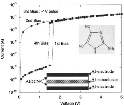
with metal nano-particle [19-20]. Yang Yang et al proposes a more promising device
with sandwich structure of organic/ core-shell nano-clusters/ organic [21]. In their
study, they use AIDCN as matrix and interpose a thin Al layer which is oxidized
during thermal evaporation and formed Al nano-clusters. The device structure and
resistive switching characteristics are shown in Fig 1.4. According to measurements
of electrical characteristics and AFM image of Al nano-clusters as shown in Fig 1.5,
they evaluate that the mechanism of resistive switching is ascribed to charging and
decharging of carriers in Al nano-clusters. Due to the charging of carriers in Al
nano-cluster, the organic thin films will be polarized and then a built-in electrical filed
is formed. This built-in electrical filed induced large amount of carrier pass through
thin films, and this device is switched to high conductance state (ON state) from
initial low conductance state (OFF state). In addition, this device with sandwich
structure can exhibit high on/off current ratio about six orders in magnitude (106)
7
Fig. 1.4: Current-voltage characteristics of AIDCN/Al nano-clusters/AIDCN
sandwich structure.
Fig. 1.5: AFM image of Al nano-cluster
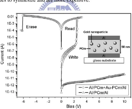
In the other hand, some research groups have proposed that organic RRAM
material with Au nano-particles. H. T. Lin et al. synthesized PCm
(4-Cyano-2,4,4-trimethyl-2-methylsulfanylthio- carbonylsulfanyl-poly (butyric acid
1-adamantan-1-yl-1-methyl-ethyl ester) with Au nano-particles as the active layer of
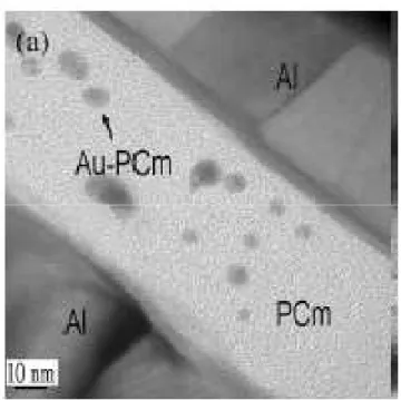
the organic RRAM [22]. The current-voltage characteristics with/without Au
nano-particles and the TEM image with Au nano-particles in PCm are shown in Fig.
1.6 and 1.7, respectively. Au nano-particles synthesized with parylene-C by B. Park
et al. [23] and Au nano-particles are blended in PVK by P.Y. Lai et al. are also be
demonstrated successfully as memory devices [24]. However, these materials need
specific techniques to synthesize and are more expensive.
Fig. 1.6: Current-voltage characteristics of Al/PCm: Au nano-particles/Al sandwich
9
Fig. 1.7: Cross session TFM image of Au nano-particles in PCm matrix.
Some proposed that memory effect and resistive switching of organic RRAM
come from its organic materials. Donor-Acceptor typed materials such as
m-NBMN/DAB, DC-BDCP complex…etc have been demonstrated as the active
layers of the organic RRAM. Y. Ma et al. investigated the arrangement of the donor
and the acceptor unit in molecular structure affected the device performance [25].
They classify that the devices based on the D–π–A–π–D molecule exhibit better
write–read–erase characteristics with a high ON/OFF ratio than devices based on the
A–π–D–π–A molecules.
Charge transfer complexes such as copper 7, 7_, 8,
RRAM. According to the current research results, Cu-TCNQ acts as solid ionic
conductor (SIC) providing mobile Cu cations, indicates that the mechanism originates
from growth and dissolution of conductive Cu filamentary paths [26]. In order to
improve the electrical properties of Cu-TCNQ-based device, a porous oxide layer
need to add in the device architecture. R. Muller et al. report an inverted device
structure which improves the possible damage of Cu-TCNQ layer during the oxide
deposition, and they also investigate the device performance with various porous
oxides such as SiO2, Al2O3, HfO2, and ZrO2. The mechanism of Cu-TCNQ-based
organic RRAM is interpreted by growth and dissolution of conducting filamentary
paths, and it provides another choice for next generation memory device. However, it
needs complicated device architecture and/or expensive process equipments such as
atomic layer deposition (ALD) to grow the dedicated layer.
1.3.
Models of Carrier Transport
1.3.1.
Fowler-Nordheim Tunneling
As depiction in Fig. 1.8, when applied a bias on device, the barrier potential will
drop. If we increase the applied bias, the barrier potential will reduce dramatically that
cause carrier tunnel through the triangle barrier. The current through the device in
case of F-N tunneling is given by [27]:
where Φ is the energy barrie
tunneling distance, m* is the reduced mass of
1.3.2.
Poole-Frenkel Emission
If the dielectrical layer contains lots of defects, carrier transport is hopping
between defects under a bias
case of P-F emission is given by
I=C V exp[
where Φ is the energy barrier height,
V is applied bias, ε is the t
11
is the energy barrier height, q is electronic charge, V is applied bias,
tunneling distance, m* is the reduced mass of the charge carrier, and C is a constant.
Fig. 1.8: Depiction of F-N tunneling
Frenkel Emission
layer contains lots of defects, carrier transport is hopping
between defects under a bias as shown in Fig. 1.9. The current through the device in
is given by [27]:
I=C V exp[-q/kT(Φ-(qV/πεl)1/2)] (Eq. 1.2)
barrier height, q is electronic charge, k is Boltzmann constant
is the tpermittivity, T is the temperature, and C is a constant. q is electronic charge, V is applied bias, d is the
the charge carrier, and C is a constant.
layer contains lots of defects, carrier transport is hopping
current through the device in
Boltzmann constant,
1.3.3.
Schottky Emission
Schottky emission is also called thermionic
carrier increases due to the absorption of thermal energy which cause
across the barrier as shown
given by:
I=A* T
where Φ is the energy barrier height,
V is applied bias, ε is the
Richard son constant.
Fig. 1.9: Depiction of P-F emission
Schottky Emission
is also called thermionic emission. The kinetic energy of
carrier increases due to the absorption of thermal energy which cause
across the barrier as shown in Fig. 1.10. The device in case of Schottky
I=A* T2 exp[-q(ΦB-β V1/2)/kT] (Eq. 1.3)
is the energy barrier height, q is electronic charge, k is Boltzmann constant
is the permittivity, T is the temperature, and A*
The kinetic energy of
s carriers inject
Schottky emission is
Boltzmann constant,
Fig. 1.10:
1.3.4.
Space Charge
Following are some as
1. The distribution of the
2. Neglect the diffusion of charge carriers
3. No recombination of
4. Neglect the thermal equilibrium charge car
The current through the device in case of
, and for the trap case is given by
Ispc
where µ is mobility, L is thickness
nf is the density of free carrier
13
Fig. 1.10: Depiction of Schottky emission
Space Charge Limited Current (SCLC)
some assumptions:
1. The distribution of the electric is uniform
2. Neglect the diffusion of charge carriers
3. No recombination of holes and electrons (monopolar injection)
4. Neglect the thermal equilibrium charge carriers
The current through the device in case of trap-free is given by [28]:
Ispc=(9/8) ε εo µV2/L3 (Eq. 1.4)
is given by [28]:
spc=(9/8) (nf/nf+nt)ε εo µV2/L3 (Eq. 1.5)
thickness, V is applied bias, εεo is the dielectrical
density of free carrier, and nt is density of trapped carrier.
1.4.
Motivation
In recent years, the demands of cost down in production lines and products are
becoming most important for device production. The selection of materials and design
of device structure are two of the key points to reduce cost. Therefore, we want to
demonstrate a potential resistive random access memory (RRAM) with cheap
materials and simple fabrication process which can integrates with the well
developing process in semiconductor industry nowadays. Moreover, we expect the
RRAM can apply to organic electronic products and even manifest the flexible
property.
In this work, we demonstrate an inorganic RRAM with low cost materials and
simple MIM structure of Ag/SiO2/p+-Si. Furthermore, we improve the endurance of
device by post-annealing treatment on SiO2 thin film. The performance and
mechanisms of devices are also investigated. Later, we fabricate organic RRAM with
bi-layer and tri-layer structure, respectively and both devices exhibit high ON/OFF
current ratio. Moreover, we observe the endurance improvement by substituting the
15
Chapter 2.
Inorganic RRAM Using Sputtered
SiO
2films
In this chapter, we focus on the research on Ag/SiO2/p+-Si structure with
different post-annealing SiO2 conditions. We observe that the device with RTA 800oC
exhibits the best performance of a memory device. Furthermore, we observe a
transition of mechanism for the high conductance states which are different from the
filamentary mechanism dominated RRAM with MIM structure.
2.1.
Fabrication of the RRAM with Ag/SiO
2/p
+-Si
Structure
The metal-insulator-metal (MIM) device structure of the inorganic RRAM in this
study is shown in Fig. 2.1. First, p+-type silicon substrate is cleaned according to a
standard RCA clean process. Then, silicon dioxide (SiO2) is deposited onto cleaned
p+-type silicon substrate at 5x10⁻³ torr using sputter at room temperature. The
sputtering power is at 100W, and the thickness is fixed at 100nm. After deposition,
two samples are treated as post-annealing using rapid thermal annealing (RTA) with
600oC and 800oC, respectively. Finally, an Ag electrode, 100nm thick is evaporated
through metal mask with 2mm x 2mm square pattern onto as-deposited, 600oC and
800oC RTA treated samples. The parameters of fabrication process are shown in Table
Fig. 2.1: Schematic diagram of
on SiO2 thin film: (a) as-deposited, (b) RTA
Table 2.1: The parameters of fabrication process of Device
SiO2 thin film
RTA temp.
Electrode (Ag)
2.2.
Electrical Characteristics
In our experiment, the
Hewlett Packard 4156A (HP 4156A) semiconductor
The p+-silicon substrate is
electrode. In addition, the scanning interval of voltage
sweeping mode. Fig. 2.2
and 800oC RTA treated samples, respectively
: Schematic diagram of Al/SiO2/p+-Si structure with different RTA conditions
deposited, (b) RTA 600oC, (c) RTA 800oC.
The parameters of fabrication process of Al/SiO2/p+-Si
Sample A Sample B Sample C
100nm
as deposited 600oC 800o
100nm
Characteristics of Ag/SiO
2/p
+-Si
RRAM Devices
n our experiment, the electrical characteristics of devices are measured using
Hewlett Packard 4156A (HP 4156A) semiconductor analyzer in ambient environment.
is grounded, and all bias conditions are applied on the
In addition, the scanning interval of voltage is set to 100mV per step in
Fig. 2.2 shows the electrical characteristics of as-deposited, 600
RTA treated samples, respectively. Initially, this device ke
with different RTA conditions
Si devices Sample C o C
RRAM Devices
measured using a in ambient environment., and all bias conditions are applied on the silver
set to 100mV per step in
deposited, 600oC
17
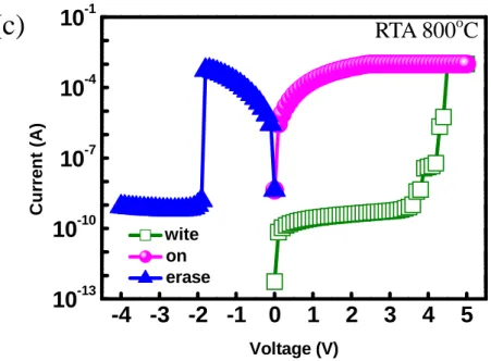
conductance state with low current level. However, when sweeping voltage exceed to
threshold voltage, 4V, 4V and 4.5V, which are individually corresponding to
as-deposited, RTA 600oC and 800oC treated samples, an abruptly increase of current is
observed. Then, devices keep at high conductance state with a high current level. The
sweeping process switches the device form low conductance state (OFF state) to high
conductance state (ON state), which is called writing process (green squares line).
When the sweeping voltage from 0V to 5V is applied again, these devices still hold at
high conductance state with high current level, which is called reading process
(magenta circles line). At third sweeping process, the reverse voltage from 0V to -4V
is applied. A noticeable drop of current from high conductance state to low
conductance state is observed. After the reducing of current, all devices are turn back
and kept at low conductance state with a low current level, which is called erasing
process. The parameters of performance of as-deposited, RTA 600oC and 800oC
treated samples are listed in Table 2.2. The Vt, Vth, and ON/OFF current ratio increase
-4 -3 -2 -1
0
1
2
3
4
5
10
-1310
-910
-510
-1 write on erase C u rr e n t (A ) Voltage (V)-4 -3 -2 -1
0
1
2
3
4
5
10
-1310
-1010
-710
-410
-1 C u rr e n t (A ) Voltage (V) write on eraseRTA 600
oC
as-deposited
(a)
(b)
19
-4 -3 -2 -1
0
1
2
3
4
5
10
-1310
-1010
-710
-410
-1 wite on erase C u rr e n t (A ) Voltage (V)Fig 2.2: The current-voltage characteristics of Al/SiO2/p+-Si structure with different
RTA conditions on SiO2 thin film: (a) as-deposited, (b) RTA 600oC, (c) RTA 800oC.
Table 2.2: The parameters of electrical measurements of Al/SiO2/p+-Si devices
Condition ON/OFF ratio Transition Voltage Threshold Voltage
as-deposited 105 ~2.5V 4V
600oC RTA 105 ~3V 4V
800oC RTA 106 ~4V 4.5V
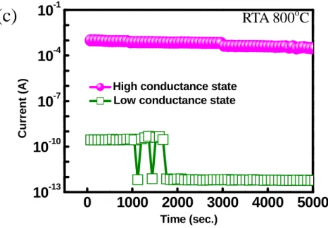
Fig. 2.3 shows the long retention time over 5000 seconds of samples with
different RTA conditions, and exhibited quite stable ON/OFF current ratio without
any degradation during the retention time measurement. The current level of ON and
RTA 800
oC
OFF states for samples with different RTA conditions in retention time measurement
are shown in Table 2.3.
0
1000 2000 3000 4000 5000
10
-1310
-1010
-710
-410
-1High conductance state Low conductance state
C u rr e n t (A ) Time (sec.)
0
1000 2000 3000 4000 5000
10
-1310
-1010
-710
-410
-1High conductance state Low conductance state
C u rr e n t (A ) Time (sec.)
as-deposited
(a)
RTA 600
oC
(b)
21
0
1000 2000 3000 4000 5000
10
-1310
-1010
-710
-410
-1High conductance state Low conductance state
C u rr e n t (A ) Time (sec.)
Fig 2.3: The retention times of Al/SiO2/p+-Si structure with different RTA conditions
on SiO2 thin film: (a) as-deposited, (b) RTA 600oC, (c) RTA 800oC.
Table 2.3: The measurements of retention time of Al/SiO2/p+-Si structure with
different RTA conditions
Condition ON current OFF Current Retention time
as-deposited 10-4 10-9 over 5000s
600oC RTA 10-3 10-9 over 5000s
800oC RTA 10-3~10-4 10-10~10-13 over 5000s
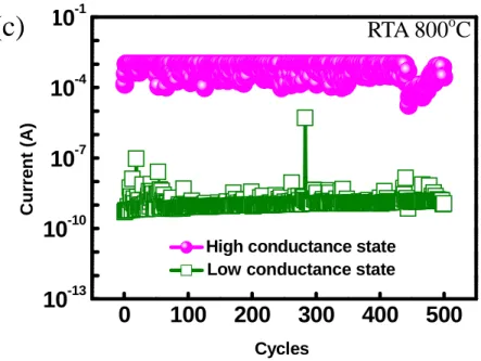
The cycle times of (operation), also called endurance test, is one of the most
important properties about the performance of a memory device. For investigation,
RTA 800
oC
the writing, reading, erasing and reading processes are executed in sequence by 5V,
1V, -4V, and 1V AC pulse for devices with different RTA conditions. To ensure the
consistence of measurement, here we apply the same writing, erasing, and reading
voltages on all devices. As shown in Fig. 2.4, the cycles of as-deposited, RTA 600oC
and 800oC treated samples are 80, 90, and 280 times, respectively. We observe that the
cycles increase with increasing RTA temperature, and the high and low conductance
currents are becoming more stable with increasing RTA temperature, especially at
800oC. Obviously, the as-deposited device shows a large perturbation between the
high and low conductance current, and device with RTA 800oC treatment shows the
most cycle times and best performance. In short, the endurance of Ag/SiO2/p+-Si
structure is improved by increasing RTA temperature on SiO2 thin film. The current
levels of ON and OFF states with different RTA conditions in endurance
23
0
20
40
60
80
100
10
-1310
-1010
-710
-410
-1High conductance state Low conductance state
C u rr e n t (A ) Cycles
0
20
40
60
80
100
10
-1310
-1010
-710
-410
-1High conductance state Low conductance state
C u rr e n t (A ) Cycles
as-deposited
(a)
RTA 600
oC
(b)
0
100
200
300
400
500
10
-1310
-1010
-710
-410
-1 C u rr e n t (A ) CyclesHigh conductance state Low conductance state
Fig 2.4: The write-read-erase-read cycles of Al/SiO2/p+-Si structure with different
RTA conditions on SiO2 thin films: (a) as-deposited, (b) RTA 600oC, (c) RTA 800oC.
Table 2.4: The measurements of endurance of Al/SiO2/p+-Si structure with different
RTA conditions
Condition ON current OFF Current Cycles
as-deposited 10-4 10-6~10-9 80
600oC RTA 10-3~10-5 10-7~10-9 90
800oC RTA 10-3~10-4 10-7~10-10 280
RTA 800
oC
25
2.3.
Mechanism and Discussion
2.3.1.
Mechanism
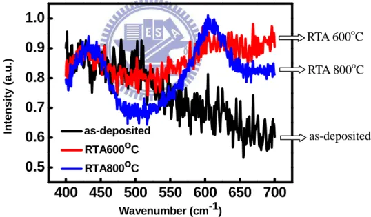
At first, we investigate the optical properties of SiO2 thin film using Raman
scattering measurements. As shown in Fig. 2.5, the intensity of the peak at 610nm
increases with increasing RTA temperature, and it indicates the 3-fold ring defects are
produced by thermal compressive stress [29]. Therefore, we know that the properties
of SiO2 thin films are varied after RTA treatment, and this result may affect the carrier
transportation and mechanism of resistive switching in the SiO2 thin films.
400 450 500 550 600 650 700
0.5
0.6
0.7
0.8
0.9
1.0
In te n s it y ( a .u .) Wavenumber (cm-1) as-deposited RTA600oC RTA800oCFig. 2.5: Raman spectrum of SiO2/p+-Si structure with as-deposited, RTA 600oC, and
RTA 800oC treatments on SiO2 thin films.
The formation of conductive filamentary paths in oxide films dominates the
resistive switching has been widely discussed and proposed. To verify the mechanism as-deposited RTA 600oC RTA 800oC
of resistive switching of the as
force microscope (c-AFM) to scan the SiO
2.6 shows the c-AFM image of the as
channels are observed. This result indicate
similar conductive filamentary property in the high conductance state. However, such
few conductive channels are probably not the only source
resistive switching.
resistive switching of the as-deposited SiO2 thin film, we use the conductive atomic
AFM) to scan the SiO2 thin film, which keeps at ON state
AFM image of the as-deposited SiO2 thin film, a few conductive
his result indicates the as-deposited SiO2 thin film m
similar conductive filamentary property in the high conductance state. However, such
few conductive channels are probably not the only source, which is
conductive atomic
keeps at ON state. Fig.
thin film, a few conductive
thin film may have
similar conductive filamentary property in the high conductance state. However, such
27
Fig. 2.6: The c-AFM images of SiO2/p+-Si structure: (a) 2-D, and (b) 3-D.
If the conductive filamentary property originates from silver cations, we can
expect the current in high conductance state will decrease with increasing temperature
due to the metallic property. To verify the point above mentioned, the current-voltage
measurements of as-deposited, RTA 600oC, and 800oC treated samples under different
temperature are investigated. As shown in Fig. 2.7, the current-voltage relation versus
temperature shows a clear independence, it suggests the carrier transport in high
conductance state isn’t dominated by metallic filamentary path. In addition, the
temperature-independent property also implies the high conductance current, in the
300
320
340
360
380
400
10
-710
-610
-510
-410
-310
-2 O N -s ta te C u rr e n t (A ) Temperature (K) as-deposited RTA600oC RTA800oCFig. 2.7: The current-voltage measurements of as-deposited, RTA 600oC, RTA 800oC
treated samples under various temperatures from 298K to 398K.
2.3.2.
Curve Fitting of I-V Currents
Mechanism of filamentary path formation and rupture has been proposed to
explain the resistive switching. According to the filamentary model, the high
conductance current exhibits an ohmic conduction property, it also means that current
(I) will proportion to biased voltage (V1). Therefore, we investigate the transport
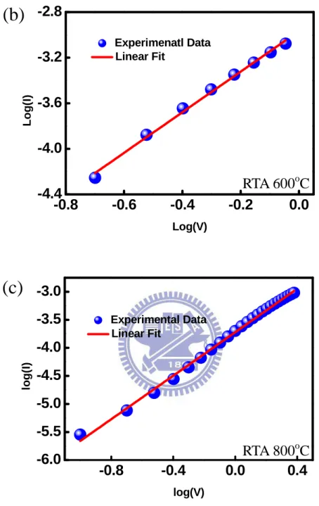
characteristics by analyzing the I-V relationship. Fig. 2.8 illustrates the I-V
relationship of the high conductance state in a log-log scale for the various treated
samples. As can be seen, all of the curves are well fitted with the linear form, meaning
29
carrier transport at the high conductance state. However, the slopes of the fitting curve
are about 1.6 and 1.8 for as-deposited, and RTA 600oC treated samples, respectively,
suggesting not only SCLC properties but also resistive properties in both samples. In
addition, the slope of the fitting curve for RTA 800oC treated sample is close to 2. Due
to the results of the curve fitting about the high conductance state, we observe a
transition of carrier transport mechanism from SCLC combined with resistive
property to pure SCLC property with different RTA conditions. The results of curving
fitting are sorted out and displayed in Table 2.5.
-0.8
-0.4
0.0
0.4
-5.5
-5.0
-4.5
-4.0
-3.5
-3.0
lo g (I ) log(V) Original Data Linear Fitas-deposited
(a)
-0.8
-0.6
-0.4
-0.2
0.0
-4.4
-4.0
-3.6
-3.2
-2.8
L o g (I ) Log(V) Experimenatl Data Linear Fit-0.8
-0.4
0.0
0.4
-6.0
-5.5
-5.0
-4.5
-4.0
-3.5
-3.0
lo g (I ) log(V) Experimental Data Linear FitFig. 2.8: Curve fitting of the I-V curves of the high conductance state of Al/SiO2/p+-Si
structure in a log-log plot: (a) as-deposited, (b) RTA 600oC, (c) RTA 800oC.
RTA 800
oC
(b)
(c)
31
Table 2.5: Fitting results of the high conductance states of Al/SiO2/p+-Si structure
with different RTA conditions
Condition Slope (S) Indicated Mechanism
as deposited 1<S<2 SCLC and ohmic property
600oC RTA 1<S<2 SCLC and ohmic property
800oC RTA S~2 SCLC
In order to confirm the probable mechanism for carrier transport in the high
conductance state, the device with RTA at 800oC is compared with the as-deposited
and RTA at 600oC ones. Since a large amount of defects exist in SiO2 thin films, the
defects should be very close to each other. When we applied a suitable bias on device,
the defects will form some localized filamentary paths, providing carrier transport
through the device, since that, an ohmic conduction will be observed, as shown in Fig.
2.9 (a). On the other hand, some carriers are trapped by defects but through the
filamentary paths, and the other carriers can transport through SiO2 thin film without
any influence by defects, as a result, it shows a transport property of SCLC.
According to the previous analyses, we suggest the devices with as-deposited and
the device with RTA at 800
causes a significant increase on the average distance of defects. Hence, the carriers
trapped in defects couldn’
property, as shown in Fig. 2.
Fig. 2.9: Paths of carrier transport for as
path1: conductive filaments, and (b) path2: SCLC
(b)
(a)
the device with RTA at 800oC is more condensed and contains a fewer defects, it
significant increase on the average distance of defects. Hence, the carriers
’t tunnel through defects, and then, it exhibits a pure SCLC
property, as shown in Fig. 2.10.
of carrier transport for as-deposited and RTA 600oC treated samples: (a)
path1: conductive filaments, and (b) path2: SCLC
C is more condensed and contains a fewer defects, it
significant increase on the average distance of defects. Hence, the carriers
t tunnel through defects, and then, it exhibits a pure SCLC
Fig. 2.10: Depiction of Mechanisms of carrier transport
for RTA 800oC treated sample
To elucidate the results of curve fitting of
samples and the proposed mechanisms,
It depicts that the flat band voltage (V
RTA temperature, meaning that, the total defects in SiO
increasing RTA temperature and the quality of SiO
treatment. Such results are
carrier transport mechanisms
33
Mechanisms of carrier transport in the high conductance state
treated sample.
To elucidate the results of curve fitting of the high conductance state
proposed mechanisms, the C-V characteristics are shown in Fig. 2.1
the flat band voltage (VFB) shifts from about -7V to -1V
, meaning that, the total defects in SiO2 thin film decrease with
increasing RTA temperature and the quality of SiO2 thin film is improved by RTA
are well corresponding to the previous suggestion about
mechanisms under various RTA conditions.
in the high conductance state
high conductance states in different
are shown in Fig. 2.11.
with increasing
thin film decrease with
improved by RTA
-8
-6
-4
-2
0
0.0
0.2
0.4
0.6
0.8
1.0
C /C m a x Voltage (V) as-deposited RTA 600oC RTA800oCFig. 2.11: C-V characteristics of Ag/SiO2/p-Si/Au structure of the as-deposited, RTA
600oC, and RTA 800oC treatments.
Furthermore, the low conductance currents of devices with various RTA
cinditions are fitted with Shottky emission model in log (I) versus E1/2 plots,
respectively. As shown in Fig. 2.12, a linear relationship is observed, meaning that,
the carrier injection of the low conductance currents is limited. Unsurprising fitting
results of low conductance currents are obtained due to the existence of a large barrier
35
200
300
400
500
-9.0
-8.9
-8.8
-8.7
-8.6
-8.5
Experimental Data Linear Fit L o g ( I) E1/2200
300
400
500
-9.2
-9.0
-8.8
-8.6
Experimental Data Linear Fit L o g ( I) E1/2as-deposited
RTA 600
oC
(a)
(b)
200
300
400
500
600
-9.8
-9.6
-9.4
-9.2
L o g ( I) E1/2 Experimental Data Linear FitFig. 2.12: Fitting of the I-V curve of the low conductance state of Al/SiO2/p+-Si
structure under different RTA conditions in a log (I) - E1/2 plot: (a) as-deposited,
(b) RTA 600oC, and (c) RTA 800oC.
RTA 800
oC
37
2.4.
Summary
The RRAM device performances are list in Table 2.6. The memory properties of
Ag/SiO2/p+-Si structure with different RTA conditions are investigated and the RTA
800oC device shows the better performance. Moreover, the transition of mechanism in
the high conductance state is also proposed and discussed in this study.
Table 2.6: The performance of Ag/SiO2/p+-Si structure under different RTA
conditions SiO2 (100nm) ON/OFF Ratio Retention Time Cycles Transition Voltage Threshold Voltage As-deposited 105 Over 5000s 80 ~2.5V 4V RTA (600OC) 105 Over 5000s 90 ~3V 4V RTA (800oC) 106 Over 5000s 280 ~4V 4.5V
Chapter 3.
Organic RRAM Using Metal Oxide
3.1.
Introduction
In this chapter, we fabricate two different structures of organic RRAM. One of
them is Al/AlOx/Alq3/n+-Si bi-layer structure, and the other one is
Al/Alq3/MoO3/Alq3/p+-Si tri-layer structure (sandwich structure). Both devices of
bi-layer and tri-layer structure can achieve high on/off current ratio about six orders
and four orders in magnitude, respectively. At first, we propose a simpler device
structure exhibiting the high on/off current ratio than tri-layer structure. Therefore, the
Al/AlOx/Alq3/n+-Si bi-layer structure is fabricated. However, the deposition of AlOx
needs a high temperature process, and we deposit AlOx by e-gun system in this work.
In addition, this bi-layer structure is subjected to cycling problem which is that device
can’t be written and erased for many times. Therefore, to demonstrate an organic
RRAM with low temperature process fabrication for application of electronic
products, we fabricate Al/Alq3/MoO3/Alq3/p+-Si tri-layer structure to manifest this
ideal. Moreover, we investigate the electrical properties and the electrode effect on
3.2.
Fabrication of the Organic RRAM
3.2.1.
Al/AlO
x/Alq
3The device structure of the organic
bi-layer structure interposed between anode and cathode in this study
3.1 (a). First, n+-type silicon substrate
process. Then, tris-(8-hydroxyquinoline) aluminum (Alq
is given in Fig. 3.1 (b),
vacuum below 3x10⁻⁶ torr
the Alq3 thin film are about
aluminum oxide (AlOx) with
evaporation at pressure below 4x10
Al thin film is evaporated through metal mask with 2mm x 2mm square pat
devices as top electrode.
3.1.
Fig. 3.1: (a) Schematic diagram of Al/AlO
formula of Alq3.
(a)
39
Fabrication of the Organic RRAM
3
/n
+-Si bi-layer structure
The device structure of the organic RRAM consisting of organic/metal
layer structure interposed between anode and cathode in this study i
type silicon substrate is cleaned according to standard RCA clean
hydroxyquinoline) aluminum (Alq3), whose structural formula
is evaporated onto cleaned n+-type silicon substrate
torr at room temperature. The deposition rate and thickness of
about 0.1nm/s and 45nm, respectively. Afterwards, 10nm thick
with deposition rate of 0.01nm/s is deposited by e
below 4x10⁻⁶ torr at room temperature. Finally, 100nm thick
evaporated through metal mask with 2mm x 2mm square pat
The parameters of fabrication process are shown in Table
: (a) Schematic diagram of Al/AlOx/Alq3/n+-Si structure. (b) Structural
(b)
of organic/metal-oxide
is shown in Fig.
s cleaned according to standard RCA clean
), whose structural formula
type silicon substrate in a
at room temperature. The deposition rate and thickness of
Afterwards, 10nm thick
s deposited by e-beam
Finally, 100nm thick
evaporated through metal mask with 2mm x 2mm square pattern onto
The parameters of fabrication process are shown in Table
Table 3.1: The parameters of fabrication process of Al/AlOx/Alq3/n+-Si device
Bi-layer
structure AlOx Alq3 Al electrode
Vacuum Value 4x10⁻⁶ Torr 3x10⁻⁶ Torr 6x10⁻⁶ Torr
Thickness 10nm 45nm 100nm
Evaporation
Rate 0.01nm/s 0.1nm/s 0.2nm/s
3.2.2.
Al/Alq
3/MoO
3/Alq
3/p
+-Si tri-layer structure
The organic RRAM consisted of an Alq3/ MoO3 nano-clusters/Alq3 tri-layer
structure interposed between anode and cathode is shown in Fig. 3.2 (a). First, a
p+-type silicon substrate is cleaned according to a standard RCA clean process. A 50
nm thick Alq3 thin film is evaporated onto the cleaned p+-type silicon substrate at
pressure below 3x10⁻⁶ torr at room temperature. Then, 5 nm thick MoO3, and 50 nm
thick Alq3 thin films are evaporated in sequence onto the Alq3/p+-Si. The average
deposition rate of the Alq3 thin film and that of the MoO3 layer are about 0.1nm/s and
0.01nm/s, respectively. Finally, 100nm thick Al thin film is evaporated through metal
mask with 2mm x 2mm square pattern onto Alq3/ MoO3 nano-clusters/Alq3/p+-Si as
top electrode. Furthermore, Standard device of 100nm thick Alq3 layer is also
fabricated, and device structure is shown in Fig. 3.2 (b). The parameters of fabrication
Fig. 3.2: Schematic diagram of
Standard devices of Alq3 single layer
Table 3.2: The parameters of fabrication process of Tri-layer structure Alq Vacuum Value 3x10 -6 Thickness 50nm Evaporation Rate 0.1nm/s
(a)
(b)
41diagram of (a) Alq3/ MoO3 nano-clusters/Alq3
single layer.
The parameters of fabrication process of Al/Alq3/MoO3/Alq3
Alq3 MoO3 Alq3 A
6
torr 3x10⁻⁶ torr 3x10⁻⁶ torr
50nm 5nm 50nm 0.1nm/s 0.01nm/s 0.1nm/s 3 structure. (b) 3/p+-Si device Al electrode 6x10⁻⁶ torr 100nm 0.2nm/s
3.3.
Organic RRAM with AlO
X/Alq
3Bi-layer Structure
3.3.1.
Electrical Characteristics
In our experiment, the electrical characteristics of devices are measured using a
Hewlett Packard 4156A (HP 4156A) semiconductor analyzer in ambient environment.
The n+-silicon substrate is grounded, and all bias conditions are applied to the
aluminum electrode. In addition, the scanning interval of voltage is set to 100mV per
step in sweeping mode. Fig. 3.3 shows the current-voltage (I-V) characteristics of the
fabricated device with Al/AlOx/Alq3/n+-Si Structure. First, when a negative bias from
0V to -5V is applied on the Al electrode with 100mA current compliance, the current
is in the low conductance state with a current level of 10-13~10-6A (red solid sphere
curve). As the bias is applied at about -5V, there is an abruptly increase in current.
Then the current of the device keeps at high conductance state with a current
compliance (100mA) for the applied voltage above -5V (red solid sphere curve). This
device undergoes a resistive switching from low conductance state to high
conductance state which is called writing process. Furthermore, the device always
maintains at a high conductance state no matter the voltage sweep from -10V back to
0V or from 0V to -10V. As can be see, this device exhibits two different conductance
states with an ON/OFF current ratio close to 106. Nevertheless, when applied a
43
device undergoes a resistive switching. This similar electrical transition is called
erasing process (blue open square curve). In addition, this device can be turned to
high conductance state again when a sweeping bias from 0V to -10V is applied on
device again (green open circle curve). Due to the observed electrical characteristics,
this device exhibits memory properties which are bistability and re-writability.
-10 -5 0 5 10
10
-1410
-1010
-610
-2 1st writing erasing 2nd writing C u rr e n t (A ) Voltage (V)Fig. 3.3: Typical I-V curves of the Al/AlOx/Alq3/n+-Si structure. The red (-●-) and
green (-○-) curves are 1st and 3rd voltage sweepings from 0V to -10V, respectively.
The blue (-□-) curve is reversed bias sweeping from 0V to 10V.
Retention time is the important property of the organic RRAM. The retention
time of Al/AlOx/Alq3/n+-Si structure is measured at -0.5V in a period of 80 seconds in
conductance state is 10-7A at -0.5V, while the average current level of low
conductance state is 10-12A at -0.5V. In spite of a fluctuation in high conductance state,
there is no significantly degradation for both states over 1500 seconds. This reveals
that the Al/AlOx/Alq3/n+-Si structure can maintain quite stable ON/OFF current ratio.
Such large ON/OFF current ratio can reduce reading errors and increase the device
reliability.
0 500 1000 1500
10
-1310
-910
-5High conductance state Low conductance state
C u rr e n t (A ) Time (s)
Fig. 3.4: Retention measurement of the reported Al/AlOx/Alq3/n+-Si structure.
3.3.2.
Mechanism
The mechanisms of organic RRAM has been widely investigated and proposed.
Charging and decharging of carriers in charge trapping centers, formation and fracture
and reduction of solid electrolyte
However, the exact mechanisms are still not clearly understood and under debate
According to the electrical
different from electrical
mechanism of filamentary paths formation
To further investigate the mechanism of
Al/AlOx/Alq3/n+-Si structure
AlOx or Alq3 as shown in Fig 3.
3.2.1.
Fig. 3.5: (a) Schematic diagram of
structure.
The electrical characteristics of
structure are shown in Fig. 3
resistive switching properties observed in both
(a)
45
and reduction of solid electrolyte…etc are addressed to interpret for
wever, the exact mechanisms are still not clearly understood and under debate
electrical characteristics observed in this work, it
electrical characteristics of filamentary paths dominated. The
ilamentary paths formation is described in section 1.2.2.
To further investigate the mechanism of electrical characteristics of the
Si structure, we also fabricate two kinds of samples with single layer
as shown in Fig 3.5. The fabrication parameters are described in se
Schematic diagram of the Ag/Alq3/n+-Si structure, (b) the
characteristics of Ag/Alq3/n+-Si structure and
Fig. 3.6 and Fig. 3.7, respectively. As can be seen, there
properties observed in both of the Ag/Alq3/n+-Si structure
(b)
for their work.
wever, the exact mechanisms are still not clearly understood and under debate yet.
s observed in this work, it’s totally
characteristics of filamentary paths dominated. The
ion 1.2.2.
characteristics of the
, we also fabricate two kinds of samples with single layer
described in section
the Ag/AlOx /n+-Si
and Ag/AlOx/n+-Si
be seen, there are no
Ag/AlOx /n+-Si structure. These results indicate that neither filaments in AlOx layer
nor Alq3 single layer is the origin of resistive switching. Therefore, we suggest that
the resistive switching is attributed to charge trapping and detrapping in the interface
defects between the Alq3 and AlOx thin films.
-10
-8
-6
-4
-2
0
10
-1210
-810
-410
0 1st sweeping process 2nd sweeping process C u rr e n t (A ) Voltage (V)Fig. 3.6: Current-voltage (I-V) curves of the Ag/AlOx/n+-Si structure.