實心與空心奈米金字塔陣列之製備及其抗反射特性研究
Synthesis of Solid and Hollow Nanopyramid Array with
Antireflective Properties
研 究 生:魏宜生
Student:I-Sheng Wei
指導教授:柯富祥 教授 Advisor:Dr. Fu-Hsiang Ko
國 立 交 通 大 學
奈 米 科 技 研 究 所
碩 士 論 文
A ThesisSubmitted to Institute of Nanotechnology College of Engineering
National Chiao Tung University in partial Fulfillment of the Requirements
for the Degree of Master
in
Nanotechnology
July 2008
Hsinchu, Taiwan, Republic of China
Acknowledgment
首先還是要謝謝柯博這兩年來的諄諄教誨與指導,接下來對於佳典學長這兩 年不論是生活上的照顧以及實驗上的指點,都讓我銘記在心。俊琪學長與其昌學 長及銘清也指導了我不少實驗上的缺失,實驗室的同學們,謝謝你們這兩年的照 顧,中書的好相處,皮皮的貼心,依蓁的細膩,美蓉的直率,鄭捷的博通,丁丁 的率真,都是伴隨著我這兩年的時光。當然還要感謝奕農群芳以及志杰學長姐在 我剛進實驗室時候的照顧,以及京璋玟菲柏軒薏卉這群貼心的學弟妹。最後要感 謝的是小松的陪伴以及我的父母親,沒有偉大的父母親,我的學生生涯不會過的 如此順利。最後,是要感謝的人太多了,那就謝天吧。實心與空心奈米金字塔陣列之製備及其抗反射特性研究
研究生:魏宜生 指導教授:柯富祥 教授
國立交通大學奈米科技研究所 碩士班
摘 要
近年來,研究零維奈米結構陣列的吸引與日俱增,因為他們獨特
的物理和化學特性。其中,空心的奈米材料表現出很大的潛力應用在
光電、藥物傳遞媒介、人工細胞、光子晶體。在這篇研究中,我們發
展出一套新穎的方法透過陽極氧化鋁模板來自組裝產生實心與空心
之氧化鉭的規則奈米金字塔陣列。金字塔陣列是由陽極氧化鋁模板側
壁所定位,而空心的機制是由於氣體膨脹所造成。有趣的是,實心的
奈米金字塔陣列在矽基板上有非常良好的抗反射效果,是由於其漸進
的非均質組成所造成。此外,空心金字塔陣列具有可調控的光學性
質。可利用嚴格耦合波分析有效的模擬出準確的光學性質,在未來上
也可利用其技術在不同基板上定做出全波段抗反射膜,如:玻璃及石
英等等。
Synthesis of Solid and Hollow Nanopyramid Array with
Antireflective Properties
Student : I-Sheng Wei
Advisor : Dr. Fu-Hsiang Ko
Institute of Nanotechnology
National Chiao Tung University
Abstract
Zero-dimensional nanostructure arrays have attracted growing interests due to their enhanced properties and become building blocks for many advanced applications. In particular, recent researches of hollow 0-D nanostructures are of great importance for potential applications in drug-delivery carriers, artificial cells, photonic building blocks, catalysis, and chemical storage. In this report, a novel strategy for fabricating the self-organized, solid and hollow nanopyramid-array tantalum oxide was investigated with anodic alumina film to serve the template. The mechanism of the growth of pyramidal nanostructure localized by the side wall of the alumina also has been proposed while the gaseous pressure expanded the hillock and left a void inside to form hollow structure with thin tantalum metal. Interestingly, solid nanopyramid-array coated on silicon substrate shows well antireflective property resulted from gradient change of non-homogeneous composition. Besides, the reflectivity of hollow nanopyramid-array shows the tunable optical properties. The rigorous coupled wave analysis (RCWA) simulation predicted the results effectively and showed potentiality to customization of various antireflective coating, especially for low-n substrate such as glass or quartz.
Contents
Acknowledgment………i Chinese Abstract……….ii Abstract……….iii Contents……….iv List of Figures………vi Chapter1: Introduction………...1 1.1 General Introduction………1 1.2 Antireflective Coating………..2 1.3 Moth-Eye Effect………...5 1.4 Hollow Nanostructure………..7 1.5 Motivation………8Chapter 2: Literature Review……….9
2.1 Zero-Dimensional Nanostructure by AAO template………9
2.2 Fabrication of Hollow Nanostructure……….12
2.2.1 Colloidal Template Synthesis………13
2.2.2 Template-free Synthesis ………...18
2.3 Subwavelength Antireflection Coating………..21
2.3.1 Antireflection Coating on Solar Cell……….21
2.3.2 Antireflection Coating on Flat Panel Display………25
Chapter 3: Experimental Methods………...29
3.2 Electrochemical Process……….31
3.3 Specimen Analysis……….33
3.4 Rigorous Coupled Wave Analysis (RCWA) ………..…35
Chapter 4: Solid Nanopyramid Arrays………39
4.1 General introduction………...39
4.2 Morphology of solid nanopyramid arrays………..40
4.3 Mechanism of solid nanopyramid growth………..45
4.4 Composition Analysis……….46
4.5 Antireflective properties……….48
Chapter 5: Hollow Nanopyramid Arrays……….53
5.1 Morphology of hollow nanopyramid arrays………...…53
5.2 Mechanism of hollow nanopyramid growth………..56
5.3 Antireflective properties……….58
Chapter 6: Conclusions………..65
List of Figures
Figure 1-1………4 Reflection and transmission coefficients of an optical coating
Figure 1-2………5 SEM micrographs of corneal nipple arrays of moth eyes. Scale bar (a) 10 μm (b) 500 nm
Figure 1-3………..6 The sub-wavelength structure of moth’s eyes.
Figure 2-1………..9 Schematic drawing of the idealized structure of anodic porous alumina.
Figure 2-2………10 (a) schematic process used to fabricate nanodots arrays on surface using alumina template. (b) Ni nanodot arrays on Si wafer.
Figure 2-3……….11 (a) schematic process used to fabricate nanodots arrays on surface using alumina template. (b) Au nanodot arrays on Si wafer
Figure 2-4………12 (a) SEM image of nanodot in 1.8 M sulfuric acid at (A) 5 V, (B) 10 V, (C) 15 V, (D) 20 V, (E) 25 V, (F)30 V; 0.3 M oxalic acid at (G) 10 V, (H) 20 V, (I) 30 V, (J) 40 V, (K) 50 V, (L) 60 V. The scale bar is 100 nm. (b) The effect of applied voltage on diameter and density of tantalum oxide nanodots.
Figure 2-5………14 Illustration of the formation of the cobalt hollow sphere chainlike structure. Figure 2-6………15 (A) TEM image of the chainlike structure of hollow Co mesospheres and (B) the
corresponding nanobeam electron diffraction (NBED) pattern.
Figure 2-7………16 Schematic outline of the experimental procedure. A cross-sectional view of the cell is shown here.
Figure 2-8………17 SEM images of hollow spheres of TiO2 that were generated by templating a sol-gel
precursor solution against a crystalline array of 380 nm polystyrene beads. (A) An array of TiO2 hollow spheres after the polystyrene particles have been dissolved and
the top substrate has been separated from the cell. (B) A cross-sectional view of this array of hollow spheres, indicating the homogeneous thickness of the wall. Figure 2-9………18 An illustration of the possible formation mechanism of the hollow Ni spheres. Figure 2-10………..18 TEM images of the hollow Ni spheres.
Figure 2-11………..19 Schematic illustration of three major steps involved in the formation of PS hollow particles with holes in their surfaces.
Figure 2-12………..20 Electron microscopy images of PS hollow particles with holes in their surfaces that were derived from PS solid beads. (a), An SEM image of the original PS solid beads. (b) - (d), SEM and TEM (inset) images of PS hollow particles with holes in their surfaces. The beads in b and c were swollen by toluene.
Figure 2-13………..21 Transmission electron microscopy (TEM) image (A), selectedarea electron diffraction (SAED) pattern (inset), and field-emission scanning electron microscopy (FESEM) image (C) of core/shell-type SnO2 hollow nanostructures prepared at 150 °C for 24 h
(r=50%, c = 8.4 mM). (B) A magnified TEM image corresponding to the square-marked area in (A). (D),(E) TEM images of SnO2 hollow nanospheres
s y n t h e s i z e d u n d e r t h e s a m e c o n d i t i o n s b u t w i t h c = 4 . 7 m M . Figure 2-14………..23 SEM image of a TMAH-textured wafer after optimized etching: 20 min US+10min without agitation, 2% TMAH, 10% IPA, 80 oC.
Figure 2-15………..24 (a) SEM images showing a tilted top view of SiNTs of length 1,600 nm.(b) The reflectance of the Si wafer and the SiNTs (L =1.6 μm) as a function of angle of incidence using s- and p-polarized light of 632.8 nm wavelength.
Figure 2-16………..24 Scanning microscope photographs of the Si surface after FAB etching For an oblique view from 45°.The measured reflectivity spectra of the SWS samples fabricated by the process shown in Figure 2-20.
Figure 2-17………..26 (a) SEM image of top morphology of PMMA latex particles on glass slide. The particle layer was formed by spin coating 5W% PMMA latex at 4000 rpm (b) AFM images of the PMMA latex particles on glass slides spin coated at 1000 rpm (c) Transmission spectra of glass slides spin coated with PMMA latex: 1, uncoated; 2, single side coated; 3, both sides coated.
Figure 2-18………..27 SEM characterization of a single PEI/tunicate bilayer adsorbed on a surface of a Si wafer with 1 min PEI and instantaneous tunicate immersions.
Figure 2-19………..28 UV-vis characterization of PEI/CNWs assembly on a microscope glass slide: (A) compilation of absorbance spectra for the first 12 bilayers, (B) absorbance at 400 nm
as function of bilayer number.
Figure 3-1………..………..29 Experimental flowchart for the fabrications and analyses of TaOx hollow nanodot
arrays.
Figure 3-2………..…..30 Schematic diagram of fabrication of the tantalum oxide nanodot arrays: (A) prestructured sample, (B) first anodic oxidation step, (C) second anodic oxidation step and hollow nanodot arrays formation, and (D) hollow nanodot arrays after removing alumina film.
Figure 3-3………..………..32 The schematic diagram of experimental setup for the aluminum electropolishing and anodization.
Figure 3-4………..………..37 (a) The geometry of the diffraction configuration for RCWA. (b) Top view of the unit cell of a circular 2D periodic grating.
Figure 3-5………....38 The periodic structure with an arbitrary profile can be approximated as a stack of lamellar gratings in RCWA
Figure 4-1………..………..41 Top-view SEM image of the porous anodic alumina film anodizing after pore widening in 5-wt% H3PO4.
Figure 4-2………42 Slide-view SEM image of the tantalum oxide nanopyramidal arrays with 30 s anodization time.
Figure 4-3………43 Slide-view SEM image of the tantalum oxide nanopyramidal arrays with 35 s
anodization time.
Figure 4-4………43 Top-view SEM image of the tantalum oxide nanopyramidal arrays.
Figure 4-5………44 TEM image of the tantalum oxide nanopyramidal arrays under the porous alumina film, the inset is the SAED image.
Figure 4-6………45 Schematic diagram to describe the formation mechanism of the tantalum oxide nanopyramidal arrays at the Ta/Al interface.
Figure 4-7………48 Ta 4f XPS of tantalum oxide nanopyramids with depth profiles. Ar+ sputtering for different etching times.
Figure 4-8………49 The broadband reflectance spectra for the blank silicon wafer, anodic tantalum oxide film, RCWA simulation and measured result of TaOx nanopyramid arrays.
Figure 4-9………51 Refractive indexes of blank silicon and substrate after removing upper structure. Figure 4-10………..51 Schematic concept of tantalum oxide nanopyramid arrays for antireflective coating. The degree of oxidation in TaOx and surface silicon result in smooth changes of refractive index from air, nanostructures to substrate.
Figure 5-1………53 SEM images showing a tilted top view of hollow nanopyramids
Figure 5-2………54 SEM images showing a tilted top view of hollow nanopyramids
SEM images showing a tilted top view of hollow nanopyramids
Figure 5-4………55 Cross section SEM image of the hollow nanopyramidal arrays with AAO above. Figure 5-5………55 TEM image of the hollow tantalum oxide nanopyramid arrays under the porous alumina film
Figure 5-6………56 Schematic diagrams to describe the formation mechanism of the hollow nanopyramidal arrays at the Ta/Al interface
Figure 5-7………57 (a) SEM image of the inverted and reduced barrier layer. Anodization for this structure was performed at 100 V, yet the same barrier layer features were observed at lower anodizing voltages on n-type Si. The white bar is 200 nm long. (b) Field-emission scanning electron microscope (FESEM) images of fracture sections where alumina film full off the substrate.
Figure 5-8………59 The experimental reflectance of nanopyramidal arrays on AlN substrate
Figure 5-9………60 Schematic diagrams of effective medium theory for rigorous coupled wave analysis Figure 5-10………..61 The results of tanΨ and cosΔ of AlN
Figure 5-11………..61 The results of tanΨ and cosΔ of TaOx
Figure 5-12………..62 The refractive index (n) and extinction coefficient (k) of AlN.
The refractive index (n) and extinction coefficient (k) of TaOx.
Figure 5-14………..64 The RCWA-simulated reflection for a bare AlN substrate and nanopyramid-array coating with 200 nm base length
Chapter 1: Introduction
1.1 General Introduction
“There’s plenty of room at the bottom” is the title of a classic talk given on December 29, 1959, in which the great physicist Richard Feynman introduced a new field of physics to the annual meeting of the American Physical Society at the California Institute of Technology. Over 40 years ago, Feynman imagined a new physical world of ultra-small volumes and highlighted some difficulties that researchers might encounter when visiting it. His talk provided a vision for engineers and scientists to establish a new field, which—with subsequent developments in novel equipment and manufacturing skills—is know known as “nanotechnology.”
In recent years nanotechnology has become one of the most important and exciting forefront field in physics, chemistry, engineering and biology which the characteristic dimensions are below ca. 1000 nm. It shows great promise for providing us in the near future with many breakthroughs that will change the direction of technological advances in a wide range of applications. This kind of work is often called nanotechnology. Sub-micron lithography is clearly very profitable—ask anyone who uses a computer—but it is equally clear that conventional lithographic techniques will not let us prepare semiconductor devices in which individual dopant atoms are located at specific lattice sites. Although computer hardware capability has exhibited steady exponential growth for the last 50 years—and there is a fairly widespread belief that these trends are likely to continue for at least several more years—conventional lithographic techniques are beginning to reach their limits. As semiconductor devices become scaled down to ever-smaller sizes within the nano-regime, a variety of technological and economic problems arise, the rules of classical physics give way to quantum mechanics, and the term “molecular-scale”
becomes more accurate than “nanoscale.” At this point, the scaling of sizes that has successfully reduced device features from the microscale to the nanoscale reaches its limits, and, therefore, alternative manufacturing methods, materials, device structures, and architectures are required.
1.2 Antireflective Coating
Anti-reflective layer is a type of optical coating applied to the surface of lenses and other optical devices. The main use of antireflection layer is to reduce the refractive lights of lens, prisms and other optical surfaces. This improves the efficiency of the system since less light is lost. In complex systems such as a telescope, the reduction in reflections also improves the contrast of the image by elimination of stray light. In planetary, this technique is especially important.
The simplest form of antireflection coating was discovered by Lord Rayleigh in 1886 [1]. The optical glass available at the time tended to develop a spot of tarnish on its surface, due to chemical reactions with the environment. Rayleigh tested some old, slightly tarnished pieces of glass, and found to his surprise that they transmitted more light than new, clean pieces. The tarnish replaces the air-glass interface with an air-tarnish interface, and a tarnish-glass one. Because the tarnish has an index of refraction between that of glass and that of air, each of these interfaces exhibits less reflection than the air-glass interface did, and in fact the total of the two reflections is less than that of the "naked" air-glass interface.
When a ray of light moves from one medium to another, for example, when light enters a sheet of glass after traveling through air, some portion of the light is reflected from the surface between the two media. This can be observed when looking through a window, for instance, where a reflection from the front and back surfaces of the
window glass can be seen [2-5]. The strength of the reflection depends on the refractive indices of the two media as well as the angle of the surface to the beam of light. The exact value can be calculated using the Fresnel equations. When the light meets the interface at normal incidence (perpendicularly to the surface), the intensity of light reflected is given by the reflection coefficient or reflectance, R:
2 0 0 ⎟⎟ ⎠ ⎞ ⎜⎜ ⎝ ⎛ + − = s s n n n n R
n0 and ns are the refractive indices of the first and second media, respectively. The
value of R varies from 0.0 (no reflection) to 1.0 (all light reflected) and is usually
quoted as a percentage. Complementary to R is the transmission coefficient or
transmittance, T. If absorption and scattering are neglected, then the value T is always
1-R. Thus if a beam of light with intensity I is incident on the surface, a beam of
intensity RI is reflected, and a beam with intensity TI is transmitted into the medium.
For a typical situation with visible light traveling from air (n0≈1.0) into common glass
(nS≈1.5), value of R is 4%. Thus only 96% of the light (T=1-R=0.96) actually enters
the glass, and the rest is reflected from the surface. The amount of light-reflected is known as the reflection loss.
In Figure 1-1, a real situation when light travel through a window, light is reflected both when going from air to glass and at the other side of the window when going from glass back to air. The size of the loss is the same in both cases. Light also may bounce from one surface to another multiple times, being partially reflected and partially transmitted each time it does so. In all, the combined reflection coefficient is given by 2R/ (1+R). For glass in air, this is about 7.7%.
Figure 1-1 Reflection and transmission coefficients of an optical coating
Many antireflective coatings consist of transparent thin film structures with alternating layers of contrasting refractive index. The layer thickness is controlled precisely, such that it is exactly one quarter of the light's wavelength thick (λ/4). The layer is then called a quarter-wave coating, which produce destructive interference in the beams reflected from the interfaces, and constructive interference in the corresponding transmitted beams. This makes the structure's performance change with wavelength and incident angle, so that color effects often appear at oblique angles. A wavelength range must be specified when designing or ordering such coatings, but good performance can often be achieved for a relatively wide range of frequencies: usually a choice of IR, visible, or UV is offered.
1.3 Moth-Eye Effect
A moth is an insect closely related to the butterfly. Both are of the order Lepidoptera. Moth eyes have orderly bumps on their corneas which seem like “nipples.” The nipples appeared to be arranged in domains with almost crystalline, hexagonal packing [7-8]. The nipple distances were found to vary only slightly, ranging from about 180 to 240 nm,but the nipple heights varied between 0 and 230 nm [8].The nipples create an interface with a gradient refractive index between that of air and the facet lens material, because their distance is distinctly smaller than the wavelength of visible light so that the reflectance of the cornea surface is effectively reduced [9]. It was most likely an evolutionary defense against nocturnal predators.
Figure 1-2 SEM micrographs of corneal nipple arrays of moth eyes. Scale bar (a) 10 μm (b) 500 nm [8]
Figure 1-3 The sub-wavelength structure of moth’s eyes [9].
This type of coating found on a moth is just now being used commercially, such as for production of anti-reflective coatings on solid plastic and other lenses [10]. It would seem to be even more difficult to control these intricate small anti-reflective coating patterns on living tissue.
In industry, non-reflection glass with synthetic moth eye structure is developed which can reduce light reflection. Scientists are now looking at using the lens in optoelectronics and photovoltaic applications in semiconductors, including solar cells, where loss of light is a major problem. The lens also has potential uses in fiber optics, sensors and medical diagnostic devices.
1.4 Hollow Nanostructure
Nanomaterials have attracted growing interests due to their potential applications and enhanced properties. Interestingly, the physical and chemical properties of nanomaterials are influenced eventfully by their size, morphology, and structure [11-15]. The aspirations of the nanomaterials were realized through self-assembled technology with highly specific function and low-cost manufacture. In virtue of expeditious promotion in various methods, highly organized building blocks of metals, semiconductors, copolymers, organic-inorganic hybrid materials have been synthesized with each passing day [16-23].
However, controlled organization into hollow nanostructures remains to be challenged. Recently, hollow micro- and nanostructures are of great importance for potential applications in drug-delivery carriers, artificial cells, photonic building blocks, catalysis, and chemical storage [11-15]. In particular, hollow nanostructures made of metal present the surface plasmonic properties different from their solid correspondents. For example, the tunable SPR (surface plasmon resonance) band has been shown by hollow gold nanoparticles. The gold and silver nanoshell enclosing dielectric cores could be controlled over the spectral regime from visible to infrared region smoothly by varying their diameter and core/shell thickness [24-26]. The red-shifted to ~680nm of broader SPR band with increasing refractive index implied that hollow nanoparticles are much more sensitive to environmental change than solid colloid and make it an ideal platform to biochemical detector.
1.5 Motivation
Current technology relies heavily on composite materials, but in most cases, the size of the individual components have been micrometers or larger. The development of nanotechnology is driven in part by the desire to prepare materials that are only a few nanometers in size or that are made from components in the sub-micrometer regime. Improved preparations of various examples of monodisperse, porous, hollow, and/or core/shell metal and semiconductor nanoparticles or nanowires have been developed.
Graded-index coatings with different index profiles have been investigated for broadband antireflection properties, particularly with air as the ambient medium. However, because of the unavailability of optical materials with very low refractive indices that closely match the refractive index of air, such broadband antireflection coatings have not been realizable.
In this report, we propose a novel strategy for fabricating the hollow and solid nanopyramid arrays with anodic alumina film to serve as the template. Anodizing reaction proceeds in the sequence of growth of porous anodic alumina when the aluminum layer is consumed up to the underlying metal, growth of metal oxide under the bottoms of the alumina pores occurred. Using this approach, we can achieve highly ordered arrays of hollow and solid nanopyramid array with controllable graded refractive index.
Chapter 2: Literature Review
2.1 Zero-Dimensional Nanostructure by AAO template
Nanoporous anodic aluminum oxide (AAO) formed by anodization has been widely studied during the last few decades. Because of their relatively regular structure with narrow size distributions of pore diameters and interpore spacings, porous alumina membranes are used for the fabrication of nanometer scale composites
[1]. The pore structure is a self-ordered hexagonal array of cells with cylindrical pores
of variable sizes with diameters of 25 nm to 300nm with depths exceeding 100 mm depending on the anodizing conditions used. The geometry of anodic porous alumina may be schematically represented as a honeycomb structure which is characterized by a close-packed array of columnar hexagonal cells[2], each containing a central pore normal to the substrate, as shown in Figure 2-1 [3].
Figure 2-1 Schematic drawing of the idealized structure of anodic porous alumina [3].
In previous work, nanodot arrays (Figure 2-2) on surfaces have been fabricated using an extremely thin (~300nm) freestanding anodic aluminum oxide template that served as a mask for evaporation of nanodots onto the surface [4-6]. Anodic porous alumina membranes were formed by anodizing foil Al in an acidic electrolyte. In
addition to these applications, removal of the bottom part of the anodic porous alumina layer by an appropriate etching process can yield through-hole membranes. Anodic porous alumina membrane used as a mask for evaporation, and then removed the membranes. This approach has been limited to deposition of nanodots by vapor-based methods because the template is not in good contact with the underlying substrate.
Figure 2-2 (a) schematic process used to fabricate nanodots arrays on surface using alumina template. (b) Ni nanodot arrays on Si wafer [4].
High density nanoparticle arrays on surfaces have been created using a template-assisted approach. Templates were produced by evaporating aluminum onto substrates and subsequently anodizing the aluminum to produce nanoporous alumina films. Because the templates remain in intimate contact with the substrate throughout processing, they may be used with either vacuum-based or wet chemical deposition methods to direct the deposition of nanoparticles onto the underlying substrates. Here Sander et al. have produced gold nanodot arrays using evaporation. The diameter and
height of the nanoparticles can be controlled using the confining dimensions of the templates, resulting in high density arrays of nanoparticles over large areas.
Figure 2-3 (a) schematic process used to fabricate nanodots arrays on surface using alumina template. (b) Au nanodot arrays on Si wafer [7].
Our group has investigated a novel strategy for fabricating the tantalum oxide nanodot with anodic alumina film to serve the template [8]. Anodizing reaction proceeds in the sequence of growth of porous anodic alumina when the aluminum layer is consumed up to the underlying metal, growth of tantalum oxide under the bottom of the alumina pores occurred. Using this approach, we can achieve highly ordered arrays of tantalum oxide nanodot with a narrow size distribution and the controllable size. The top-view SEM images of the tantalum oxide nanodot arrays formed in various applied voltage and two different electrolytes after removing the overlying alumina film are shown in Figure 2-4(a). Two electrolytes have been selected because of the difference in the forming voltages and electrolyte-derived species, which affected the properties of the nanodots. The population density and
average diameter of nanodot were calculated and plotted in Figure 2-4(b) The nanodot diameter ranges between 15 nm and 70 nm and density ranges between 1011/cm2 and 1010/cm2.
Figure 2-4 (a) SEM image of nanodot in 1.8 M sulfuric acid at (A) 5 V, (B) 10 V, (C) 15 V, (D) 20 V, (E) 25 V, (F)30 V; 0.3 M oxalic acid at (G) 10 V, (H) 20 V, (I) 30 V, (J) 40 V, (K) 50 V, (L) 60 V. The scale bar is 100 nm. (b) The effect of applied voltage on diameter and density of tantalum oxide nanodots [8].
2.2 Fabrication of Hollow Nanostructure
Typically, hollow nanostructures are prepared by the template synthesis, including hard ones such as silica spheres [9], polymer cores [10], and reducing metal nanoparticles [11], as well as soft ones like emulsion droplets and gas bubbles [12]. The Template method, either hard template or soft one, are coated by surface precipitation or by direct surface reactions with specific functional groups on the cores to create core/shell composites [13]. The template particles are removed selectively by dissolution in the appropriate solvent or calcination at elevated temperatures to generate ceramic hollow spheres. Caruso et al., the pioneers of the layer-by-layer
consecutive deposition of oppositely charged polyelectrolytes from dilute aqueous solution onto charged solid substrates [14]. Furthermore, many synthetic methods of hollow nanostructures are developed including the nanoscale Kirkendall effect, corrosion-based evacuation and varied template-free synthesis [15]. Although the hollow structures presented by above pioneering works are very interesting, however, the processing routes usually suffer tedious synthetic procedures and time-consuming
[16]. For example, multi-step processes are needed for the synthesis of core-shell
composite particle and exchange of coating reaction for the template approach, or the repeated adsorption cycles for the layer-by-layer method. Mostly, the syntheses of the hollow nanostructures are dispersed in chemical solution [17]. These solution-based synthetic methods are hardly to be integrated into the state-of-the-art semiconductor technology [18]. Ideally, one would prefer a one-step method for controlled preparation of hollow structures in a wide range of sizes.
2.2.1 Colloidal Template Synthesis
Colloidal particles with hollow interiors play important roles in micro encapsulation—a process that has found widespread use in applications such as controlled release of drugs, cosmetics, inks, pigments or chemical reagents; protection of biologically active species; and removal of pollutants.[19] The hollow particles are most commonly prepared by coating the surfaces of colloidal templates with thin layers of the desired material or its precursor, followed by selective removal of the templates by means of calcinations or chemical etching. This simple and straightforward approach works for a variety of materials that include polymers, ceramics, composites and metals.
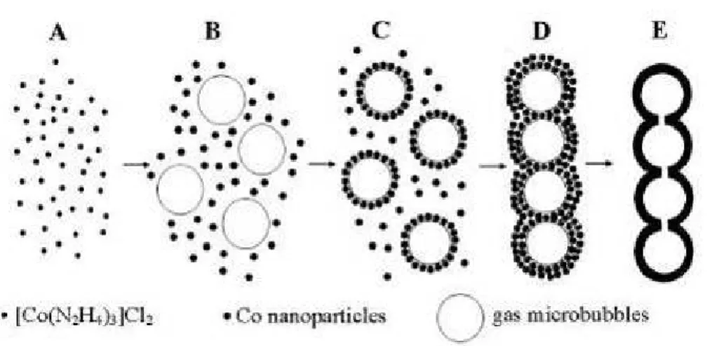
Here is a method for the synthesis of chainlike nanostructures consisting of Co hollow mesospheres in a polymer solution [20]. These hollow mesospheres were found
to form through the aggregation of small Co nanoparticles.This method, using gas bubbles and PVP(poly vinylpyrrolidone )as a dynamic template, has the advantages of being simple, having a high yield, and mild reaction conditions. Therefore, it represents an attractive path to large-scale assembly of metallic hollow nanospheres with a significantly enhanced magnetic coercivity at 300 K for the Co hollow nanospheres compared to the bulk value. The excellent stability, the hollow nanostructure, and the hierarchical self-assembled architecture afford a model system for fundamental investigations and promising applications in various fields of nanotechnology.
Figure 2-5 Illustration of the formation of the cobalt hollow sphere chainlike structure
Figure 2-6 (A) TEM image of the chainlike structure of hollow Co mesospheres and (B) the corresponding nanobeam electron diffraction (NBED) pattern [20].
Another effective method that is capable of forming ceramic hollow spheres with a well-defined void size and homogeneous wall thickness is reported by Ziyi Zhong et al [21]. The void size of these hollow spheres was determined by the diameter of the polystyrene template, and the thickness of the ceramic wall could be easily changed in the range of 30±100 nm by using Sol-gel precursor solutions with different concentrations.
Figure 2-7 Schematic outline of the experimental procedure. A cross-sectional view of the cell is shown here [21].
Figure 2-7 shows the schematic procedure. The crystalline array of polystyrene beads was fabricated between two glass substrates using a previously published method [22]. After the water had been removed by evaporation at room temperature, the hydrodynamic size of the polymer beads shrank by ~20 %, and the magnitude of this shrinkage is mainly determined by the electrostatic interactions among the polymer beads. The strength of such interactions strongly depends on the density of charges on the surface of each polymer bead and the total concentration of free electrolytes in the water[23]. Although the polystyrene beads were in physical contact in the dried sample, they became separated from each other when the packing cell was infiltrated with a sol-gel precursor solution by capillary action [24]. This separation was presumably caused by the repulsive electrostatic interactions among the charged particles.
Figure 2-8 SEM images of hollow spheres of TiO2 that were generated by templating
a sol-gel precursor solution against a crystalline array of 380 nm polystyrene beads. (A) An array of TiO2 hollow spheres after the polystyrene particles have been
dissolved and the top substrate has been separated from the cell. (B) A cross-sectional view of this array of hollow spheres, indicating the homogeneous thickness of the wall [22].
This is an effective route to fabricate mesoscale hollow spheres of oxide ceramics such as TiO2 and SnO2. These hollow spheres have a well-defined void size
that is determined by the diameter of the polystyrene template, and a homogeneous wall whose thickness is mainly controlled by the concentration of the sol-gel precursor solution. This procedure can also be applied to the fabrication of monodisperse, composite particles consisting of cores covered with shells of different chemical compositions.
2.2.2 Template-free Synthesis
Hollow metal nanometer spheres have been studied for years. A facile hydrothermal method for the formation of hollow Ni nanostructure is reported by Qi
Liu et al [25]. The hollow Ni nanometer sphere is fabricated via the redox reaction of
Ni(DS)2 ( nickel dodecylsulfate ) with NaH2PO2 micelle system [26]. This work is the
first concerning the synthesis of ferromagnetic metal nanometer-sized hollow spheres in aqueous solution. Such hollow Ni spheres have some promising application in the fields of magnetic materials and catalysis, etc.
Figure 2-9 An illustration of the possible formation mechanism of the hollow Ni spheres [25].
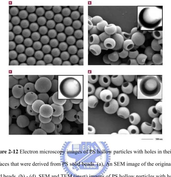
Figure 2-11 Schematic illustration of three major steps involved in the formation of PS hollow particles with holes in their surfaces [27].
Younan Xia and co-workers take polystyrene (PS) as a template to fabricate polymer hollow nanoparticles with controllable holes in their surfaces [27]. Figure 2-11 show the three major steps involved in the formation of PS hollow particles with holes in their surfaces. In the first step, PS solid beads suspended in water are swollen by toluene to expand their volumes. The system is then frozen with liquid nitrogen to create a void inside each bead as a result of volume shrinkage associated with the liquid to solid phase transition for toluene. In the last step, the system is warmed up to let the toluene evaporate at temperatures below 0 oC. A hole is formed in the surface of each PS hollow particle because of the evaporation flux of toluene.
Figure 2-12 Electron microscopy images of PS hollow particles with holes in their surfaces that were derived from PS solid beads. (a), An SEM image of the original PS solid beads. (b) - (d), SEM and TEM (inset) images of PS hollow particles with holes in their surfaces. The beads in b and c were swollen by toluene [27].
Xiong Wen Lou et al. have developed a simple one-step template- free method
for the controlled synthesis of hollow or hollow core/shell-type SnO2 nanostructures [28]. This method is based on hydrothermal treatment of stannate in a mixed solvent of
ethanol–water. With the mediation of urea or thiourea, the current method is suitable for inexpensive, mass production of SnO2 hollow nanoparticles. A novel inside-out
Ostwald ripening mechanism (growth of bigger particles at the expense of smaller ones) is proposed to account for the template-free formation of these hollow nanostructures. The as-prepared SnO2 hollow nanospheres exhibit superior lithium
batteries.
Figure 2-13 Transmission electron microscopy (TEM) image (A), selectedarea electron diffraction (SAED) pattern (inset), and field-emission scanning electron microscopy (FESEM) image (C) of core/shell-type SnO2 hollow nanostructures
prepared at 150 °C for 24 h (r=50%, c = 8.4 mM). (B) A magnified TEM image
corresponding to the square-marked area in (A). (D),(E) TEM images of SnO2 hollow
nanospheres synthesized under the same conditions but with c = 4.7 mM [28].
2.3 Subwavelength Antireflection Coating
2.3.1 Antireflection Coating on Solar CellAmorphous hydrogenated silicon nitride (a-SiNx:H) antireflection coating on crystalline silicon is today’s standard process for solar cell industry. There is a very different refractive index between air and silicon substrate which not only causes more than 30% of incident light is reflected back from the surface of single-crystalline silicon solar cells but also reduces the transformation efficiency of solar cells [29]. Over the past decade, silicon nitride has gradually replaced titanium dioxide (TiO2) as the
[30]. With the purpose to increase the light collection and the high-efficiency of silicon
solar cells, the reflection of the front surface needs to be minimized. This improvement is currently achieved by a textured surface covered by an antireflection coating. This surface pattern can be realized by different techniques:plasma etching
[31] , mechanical engraving [32], and chemical etching [33]. The last one is actually a
good compromise between cost and efficiency. Photovoltaic production widely uses potassium hydroxide (KOH) or sodium hydroxide (NaOH) as aqueous texturing solutions. These alkaline solutions etch the silicon anisotropically and form small pyramids on the silicon surface. Both the composition and the temperature of the etching solution were optimised on the basis of anisotropic etching-rate measurements on silicon samples having different crystallographic directions [34].
Hence, light collection is increased by multiple reflections. KOH and NaOH etching solutions are cost and time efficient but present some drawbacks:the potassium and sodium contaminations are detrimental for microelectronic devices, and are supposed to have the same effect on solar cell devices. A promising alternative solution is tetramethyl ammonium hydroxide ((CH3)4 NOH, TMAH) [34].
This solution is widely used in microelectronic and MEMS, because it combines high etching rate and a good anisotropic etching with a full compatibility with microelectronic technologies. Moreover, this solution is clean room compatible, nontoxic and easy to handle. TMAH solution also exhibits excellent selectivity towards silicon oxide and silicon nitride masks
Figure 2-14 SEM image of a TMAH-textured wafer after optimized etching: 20 min US+10min without agitation, 2% TMAH, 10% IPA, 80 oC [34].
Yi-Fan Huang and coworkers report a simple aperiodic array of silicon nanotips on a 6-inch wafer with a sub-wavelength structure that can suppress the reflection of light at a range of wavelengths from the ultraviolet, through the visible part of the spectrum, to the terahertz region [35]. Reflection is suppressed for a wide range of angles of incidence and for both s- and p-polarized light. The antireflection properties of the silicon result from changes in the refractive index caused by variations in the height of the silicon nanotips, and can be simulated with models that have been used to explain the low reflection from moth eyes. The improved anti-reflection properties of the surfaces could have applications in renewable energy and electro-optical devices for the military.
Figure 2-15 (a) SEM images showing a tilted top view of SiNTs of length 1,600 nm.(b) The reflectance of the Si wafer and the SiNTs (L =1.6 μm) as a function of angle of incidence using s- and p-polarized light of 632.8 nm wavelength [35].
Hitoshi Sai et al. report a robust and simple fabrication technique for Si SWS
surfaces that has the potential to become a low-cost and large-area process [36]. Anodic porous alumina masks are also used in this technique, but they are formed directly on Si wafers. SWS surfaces with a deep tapered profile are fabricated on as-cut multicrystalline Si, which is a main material in solar cell applications, as well as conventional single-crystalline Si with a polished surface. As a consequence, smoothly tapered SWS surfaces with a period of 100 nm and a height of 300–400 nm were obtained on both types of wafers. A low reflectivity below 1% was observed over a wide spectral bandwidth from 300 to 1000 nm.
Figure 2-16 Scanning microscope photographs of the Si surface after FAB etching For an oblique view from 45°.The measured reflectivity spectra of the SWS samples
[36].
2.3.2 Antireflection Coating on Flat Panel Display (FPD)
Modern optical elements need solutions for providing a surface with antireflective properties to increase the optical transmission and high image resolution. For a long time, the optical thin film coating process plays an important role. Flat panel displays encompass a growing number of technologies enabling video displays that are lighter and much thinner than traditional television and video displays that use cathode ray tubes, and are usually less than 4 inches thick. Flat panel displays balance their smaller footprint and trendy modern look with high production costs and in many cases inferior images compared with traditional CRTs. In many applications, specifically modern portable devices such as laptops, cellular phones, and digital cameras, whatever disadvantages are overcome by the portability requirements.Flat panel display industry is a highly competitive area, globally driven by the intricate balance between technical advancement toward better performance and the ever demanding production cost. Along the vertically integrated manufacturing of FPD, there always exists a technology-cost bottle neck that defines and often limits the growth of the market.
Recently, the application of antireflection optical polymer film for large area flat panel display(FPD)has been paid much attention for the reason of the market growing of LCD TV . Except traditional dry and wet coating process, another new method of subwavelength nanostructure to achieve optical antireflection effect is developed. The large area polymer film with periodic or stochastic moth eye structured array performs excellent optical antireflection property in broad band wavelength and with wide view angle. Such nanostructure antireflection technology is
simply to achieve for roll to roll mass production process and has much advantage in cost consideration in the future.
A subwavelength structured ( SWS ) surface, which is the surface-relief grating with the period smaller than the light wavelength, behaves as an antireflection surface. The SWS surface with a deep tapered shape grating especially suppresses the reflection over a wide spectral bandwidth and a large field of view. According to the analysis, antireflection properties are improved by decreasing the grating period and increasing the grating depth.
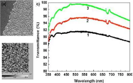
Another example of preparing antireflective coatings on glass slides by spin casting polymer latex has been fabricated by Hao Jiang et al. [37] Optical transmittances at 550 nm of 95.7% for a single-sided coating and 99.5% for a double-sided coating were achieved. Structure investigations with atomic force microscopy and scanning electron microscopy revealed that the antireflective coatings were highly porous and affected by spin speed and by the concentration and particle size of PMMA latex. Spin coating may be a better method for mass production, because of its convenience, low cost, and good reproducibility.
slide. The particle layer was formed by spin coating 5W% PMMA latex at 4000 rpm (b) AFM images of the PMMA latex particles on glass slides spin coated at 1000 rpm (c) Transmission spectra of glass slides spin coated with PMMA latex: 1, uncoated; 2, single side coated; 3, both sides coated [37].
Paul Podsiadlo and co-worker demonstrate equally effective coatings by LBL assembly of cellulose nanowires (CNWs). The morphology of CNWs is also quite remarkable. Their uniformity and high aspect ratio can be very favorably compared with synthetic nanowires (NWs) [38], while their preparation is very simple. They can be an example of naturally perfect nanostructures. Paul Podsiadlo show that the layered architecture of the coating and parallel orientation of the micronslong and stiff CNWs, with respect to the coated surface, result in formation of a porous structure with film-thickness-dependent porosity and optical properties. In simplest terms, the structure of the coating can be compared to that of a “flattened matchsticks pile”. The underlying physics of the AR effect is certainly the same as in the other AR coatings; however, the structure of LBL-assembled CNWs has a decisively new morphology.
Figure 2-18 SEM characterization of a single PEI/tunicate bilayer adsorbed on a surface of a Si wafer with 1 min PEI and instantaneous tunicate immersions [38].
Figure 2-19 UV-vis characterization of PEI/CNWs assembly on a microscope glass slide: (A) compilation of absorbance spectra for the first 12 bilayers, (B) absorbance at 400 nm as function of bilayer number [38].
Chapter :3 Experimental Method
Figure 3-1 Experimental flowchart for the fabrications and analyses of TaOx hollow
nanodot arrays.
Figure 3-1 shows experimental flowchart for the fabrications and analyses of tantalum oxide nanodot arrays. The AAO templates were prepared by the two-step anodization of the aluminum films. The tantalum oxide nanodot arrays were prepared by the anodization of the Al/Ta bilayer films. The microstructure of the AAO
Substrate
Al film deposition
Al film anodization
AAO template
AAO film removes
TaOx hollow nanodot
Ta film deposition
Ta film anodization
TEM SEM
SEM XPS SEM AFM
Al film electropolishing
Ellipsometer
templates was studies by scanning electron microscopy (SEM). The microstructure, bonding structure, chemical composition, and crystallinity of tantalum oxide nanodots were investigated by SEM, atomic force microscopy (AFM), transition electron microscopy (TEM), and X-ray photoelectron spectroscopy (XPS). The reflective properties were measured by optical spectrometer (Hitachi, U-4100). The refractive index was confirmed by a variable angle spectroscopic ellipsometer. The simulated reflection properties were analyzed by the rigorous coupled-wave analysis (RCWA) in two-dimensional nanostructure. Figure 3-2 shows the schematic diagram of fabrication of hollow nanodot arrays.
Figure 3-2 Schematic diagram of fabrication of the tantalum oxide nanodot arrays: (A) prestructured sample, (B) first anodic oxidation step, (C) second anodic oxidation step and hollow nanodot arrays formation, and (D) hollow nanodot arrays after removing
alumina film.
3.1 Films Deposition
The tantalum films for the tantalum oxide nanodots production were deposited on a cleaned aluminum nitride or silicon substrate by ultrahigh vacuum dc sputtering system (ULVAC SBH-3308). Before film deposition, the base pressure of the sputtering chamber was evacuated to approximately 6.67×10⁻⁵ Pa, and the sputtering pressure was kept at 0.85 Pa by mass flow controllers during sputtering. The Ta target used was 99.9999% pure. The Ta films were prepared at argon gas. Subsequently, an aluminum films was deposited onto the Ta films by a thermal evaporation system (ULVAC CRTM-6000) with a base pressure of 2×10⁻⁶Torr. to form Ta/Al bilayer sample. Tungsten boats were used in melting and evaporating the aluminum ingots. The tungsten boats were cleaned in a mixed solution of 20 vol.% hydrogen fluoride (HF) and 80 vol.% nitric acid (HNO3). The sample was annealing at 400oC in a
vacuum furnace with H2/N2 purge for 4 hr to recrystallize. The sample was then cut
into piece of 3×3 cm2 and electropolished in a mixed solution of 10 vol.-% H3PO4
with constant current 0.15 ampere.
3.2 Electrochemical Process
Figure 3-3 shows the schematic diagram of experimental setup for the aluminum electropolishing and anodization. A specially designed one-electrode cylindrical cell double layer glass cup was used which can let cooling water flow through. The anode was the aluminum film specimen and a graphite flake was used as the cathode.
Because edges of the aluminum film undergoing stronger electric field have a faster reaction rate than center, only a part of the film was exposed to the electrolyte through an open circle with an area of about 1.5 cm2 on the cylinder, and there was an O-ring clipped between the specimen and the tank fixed by a jig. GW laboratory power supply (model GPC-3060D) was used as the anodizing source. Subsequently, anodization was carried out in 2M phosphoric acid solution using a conventional two-electrode system connected to a power supply under a constant voltage of 110 V. All anodizing process were performed at room temperature and stirred adequately. When the anodization was nearly complete, here was a distinct color change in sample surface and decreasing in the current. The anodization was proceeded 10-s past the color change to ensure anodizing completely. Then the alumina film was removed in 5wt-% phosphoric acid solution in room temperature.
Figure 3-3 The schematic diagram of experimental setup for the aluminum electropolishing and anodization.
_
+
Al/Ta/AlN film
graphite
cathode
cooling water in cooling water out3.3 Specimen analysis
(A) SEMSEM is a very useful tool for observing surface morphology of specimen. SEM has secondary electrons or backscattered electrons detectors passing the signal to computer and forming image. In this study, the morphology and microstructure of the porous alumina films and nanodots were all characterized by a field-emission SEM (FE-SEM) (JEOL-6700) operating at 15 kV accelerating voltage.
(B) TEM
TEM image is the result of electron transmitting through the specimen. TEM reveals the interior microstructure of the specimen, and it can give the high-resolution lattice image and the electron diffraction pattern as well. In this study, the morphology and microstructure of the porous alumina films and nanodots were all characterized by A TEM (JEOL JEM-2100F) operating at 200 kV accelerating voltage. Cross-sectional specimens for the TEM analysis were prepared by mechanical polishing and subsequent argon ion milling.
(C) XPS
Surface analysis by XPS involves irradiating a solid in vacuum with monoenergetic soft X-rays and analyzing the emitted electrons by energy. The spectrum is obtained as a plot of the number of detected electrons per energy interval versus their kinetic energy. Quantitative data can be obtained from peak height or peak areas, and identification of chemical states often can be made from exact measurement of peak positions and separations. In this study, XPS was employed to analysis the chemical state of the titanium oxide nanodots. XPS analyses were performed on a Physical Electronics ESCA PHI1600 system with Al-Kα (1486.6 eV)
excitation. The background pressure during the analysis was better than 10-9Torr. Argon ion with ion energy of 5 keV was used for sputter profiling and surface clean.
(D) Ellipsometer
Ellipsometer is a versatile and powerful optical technique for the investigation of the dielectric properties (complex refractive index or dielectric function) of thin films. It has applications in many different fields, from semiconductor physics to microelectronics and biology, from basic research to industrial applications. Ellipsometry is a very sensitive measurement technique and provides unequalled capabilities for thin film metrology. As an optical technique, spectroscopic ellipsometry is non-destructive and contactless. Upon the analysis of the change of polarization of light, which is reflected off a sample, ellipsometry can yield information about layers that are thinner than the wavelength of the probing light itself, even down to a single atomic layer or less. Ellipsometry can probe the complex refractive index or dielectric function tensor, which gives access to fundamental physical parameters and is related to a variety of sample properties, including morphology, crystal quality, chemical composition, or electrical conductivity. It is commonly used to characterize film thickness for single layers or complex multilayer stacks ranging from a few angstroms or tenths of a nanometer to several micrometers with an excellent accuracy.
(E) UV-Vis spectroscopy
Ultraviolet-visible spectroscopy involves the spectroscopy of photons in the UV-visible region. It uses light in the visible and adjacent near ultraviolet (UV) and
near infrared (NIR) ranges. In this region of the electromagnetic spectrum, molecules undergo electronic transitions.
3.4 Rigorous Coupled Wave Analysis (RCWA)
The simulated reflection properties are analyzed by the rigorous coupled-wave analysis (RCWA) in two-dimensional nanostructure. Over the past 10 years the rigorous coupled-wave analysis (RCWA) has been the most widely used method for the accurate analysis of the diffraction of electromagnetic waves by periodic structures. It has been used successfully and accurately to analyze both holographic and surface-relief grating structures. It has been formulated to analyze transmission and reflection planar dielectric– absorption holographic gratings, arbitrary profiled dielectric–metallic surface-relief gratings, multiplexed holographic gratings, two-dimensional surface-relief gratings, and anisotropic gratings for both planar and conical diffraction [1-5]. The RCWA is a relatively straightforward technique for obtaining the exact solution of Maxwell’s equations for the electromagnetic diffraction by grating structures. It is a noniterative, deterministic technique utilizing a state-variable method that converges to the proper solution without inherent numerical instabilities. The accuracy of the solution obtained depends solely on the number of terms in the field space-harmonic expansion, with conservation of energy always being satisfied.
RCWA is one of the most widely used methods for the rigorous analysis of the optical diffraction by periodic gratings [6]. Figure 3-4 (a) illustrates the geometry of the diffraction configuration for RCWA. [7] The whole structure can be divided into three regions: the incident region (Region I), the grating region (Region II) and the exit region (Region III). The total electric fields in the external regions (I, III) can be
expressed as
∑
− + − Ι Ι=
+
n m z k y k x k mn mn z yn xmR
E
E
, ) ( j inc ,e
r
r
r
∑
− + − − ΙΙΙ = ΙΙΙ n m h z k y k x k mn mn z yn xm T E , )] ( [ j , e r rwhereErinc is the incident electric field; Rmn and Tmn are the electric field amplitudes
of (m,n)th reflected and transmitted orders, respectively. The wave vector components
kxn
and kym are determined from the Floquet conditions and are given by
⎟⎟ ⎠ ⎞ ⎜⎜ ⎝ ⎛ − = x x xm Λ m k k inc, 2π ⎟ ⎟ ⎠ ⎞ ⎜ ⎜ ⎝ ⎛ − = y y yn Λ n k k inc, 2π
where kinc is the wave vector of the incident field; Λx and Λy are the periods of the
grating along x and y direction, respectively. The magnetic fields in the external regions can be obtained from Maxwell’s equation
E j Hr =− ∇× r 0 1 ωμ
where μ0 is the permeability of free space and ω is the angular optical frequency.
In the grating region, its periodic permittivity can be expressed in the Fourier expansion
∑
⎟⎟⎠ ⎞ ⎜ ⎜ ⎝ ⎛ + ΙΙ = h g hy Λ gx Λ jk gh y x y x , 0 0 0 e ) , ( λ λ ε εFor a periodic circular pillar shown in Figure 3-4 (b), the Fourier coefficients εgh can
be written as ( ) ( ) ( ) 2 2 0 , 2 0 , ) ( ) ( , 1 1 2 2 1 2 1 x y r J Λ Λ r Λ Λ r gh Λ h Λ g y x y x + = ⎪⎩ ⎪ ⎨ ⎧ = − ≠ = − + ρ ε ε ε ρ πρ ρ ρ π ε ε ε
The electric and magnetic fields in the grating region can be expressed with a Fourier expansion in terms of the spaceharmonic fields
( )
( )∑
− + ΙΙ = n m y k x k mn yn xm z S E , j e r r( )
( )∑
− + ΙΙ =− n m y k x k mn yn xm z U H , j 0 0 e j r r μ εwhere ε0 and μ0 are the permittivity and permeability of free space, respectively. Smn
and Umn are the amplitudes of the (m,n)th space-harmonic fields. Finally, by applying
the Maxwell’s equation in the grating region and matching the boundary conditions at the interface of the three regions, the unknown amplitudes Rmn and Tnm of the
diffracted waves can be determined.
Figure 3-4 (a) The geometry of the diffraction configuration for RCWA. (b) Top view of the unit cell of a circular 2D periodic grating [7].
Figure 3-5 The periodic structure with an arbitrary profile can be approximated as a stack of lamellar gratings in RCWA [7]
Chapter 4: Solid Nanopyramid Arrays
4.1 General Introduction
The fabrication of nanodot arrays has attracted growing interest due to their realization in functional structures and in the field of nano-devices such as optoelectronics, information storage, and sensing [1–3]. Variety of alternative methods have been proposed for the formation of nanodot arrays such as electron beam lithographic techniques, nanoimprint [4], self-assembly of nanodot from solution [5], controlled nanoparticle growth by diffusion [6], strain-induced growth [7]. However, most of these works can be applied to only limit material systems. Since the discovery of self-ordered porous alumina in 1995 by Masuda and Fukuda [8], which consists of vertical pore channel arrays with a high density hexagonal packing structure, was obtained by anodic oxidation of aluminum in an acidic electrolyte. The pore diameters are tunable in the range of ten to several hundred nanometers, and very simple formation process making porous anodic alumina an ideal template for fabricating ordered arrays of nanostructures materials such as nanowires [9,10], nanotubes [11,12], or nanodots [13,14].
In previous work, nanodots have been fabricated by anodic alumina template as mask for evaporation of nanodots onto surface [15]. This approach has been limited to deposition of nanodots by evaporation just because of poor contact between template and underlying substrate. Moreover, during anodization an alumina barrier layer is formed at the bottom of the pores which prevent nanodots deposited directly from underlying layer. In order to use the template to deposit nanodots onto the surface, the barrier layer must be removed. Our group proposed a novel strategy for fabricating the tantalum oxide nanodot with anodic alumina film to serve the template. Anodizing reaction proceeds in the sequence of growth of porous anodic alumina when the
aluminum layer is consumed up to the underlying metal, growth of tantalum oxide under the bottom of the alumina pores occurred. Using this approach, we can achieve highly ordered arrays of tantalum oxide nanodot with a narrow size distribution and the controllable size. Based on these novel methods, we have fabricated nano-sized pyramids with very low reflectance which can apply in antireflective coatings.
4.2 Morphology
Figure 4-1 shows the top-view SEM image of the porous anodic alumina film anodizing in 0.3M oxalic acid at 40V after pore widening. The self-organized nanopores with a uniform size distribution have the interpore distance about 100 nm. Because the aluminum films in our studies were only 3 μm thick, the pore at substrate showed neither long-range order nor hexagonal arrays. It may be possible to obtain more ordered pores with a narrower size distribution by starting with thicker and fine quality films [16]. The anodic current density was steady at 8 mA/cm2 except for initial nucleate state. When the porous alumina films had been nearly completely anodized, there was a distinct color change resulting from the transparency of the porous alumina. To ensure the process was completely anodized, the power was cut off at 0.2 mA/cm2.
Figure 4-1 Top-view SEM image of the porous anodic alumina film anodizing after pore widening in 5-wt% H3PO4.
Figures 4-2 and 4-3 show the slide-view scanning electron microscopy (SEM) (JEOL JSM-6700F) images of pyramidal nanodot arrays at various anodization periods. The insufficient 30 s anodization time in Figure 4-2 cannot form the close-packed pyramid arrays and exhibits poor AR. The tantalum oxide bulges jutted out over the residual aluminum. This observation is attributed to the Al residue from the incomplete anodization. In contrast, the pyramidal structure after a 35 s anodization time with a 2×10⁹/cm2 density in Figure 4-3is very dense with an average diameter of 200 nm and an average height of 200 nm. The close-packed pyramid structure of 200 nm period, which is the surface-relief grating with a period smaller than the incident light wavelength, behaves as an advantaged AR surface. Horizontal projections of the bases look like distorted hexagons or pentagons rather than the circles under pores in Figure 4-4. In contrast, the shape of the nanostructure presented here is a pyramid instead of a hemisphere reported in other records [17]. Figure 4-5
shows the cross-sectional transmission electron microscopy (TEM) (JEOL JEM-2100F) image of the bottom of the alumina pores. An isolated pyramid structure embedded at the interface between porous alumina and the underlying layer is seen. The inset in Figure 4-5 with the selected area electron diffraction (SAED) image shows an amorphous structure of tantalum oxide pyramidal arrays, and the result conforms to the literature [18]. The chemical composition of the self-organized pyramids is expected to be the composition of nonstoichiometric TaOx with Ta2O5 at
the surface and coexistence of different oxidation states of tantalum inside [17].
Figure 4-2 Slide-view SEM image of the tantalum oxide nanopyramidal arrays with 30 s anodization time.
Figure 4-3 Slide-view SEM image of the tantalum oxide nanopyramidal arrays with 35 s anodization time.
Figure 4-5 TEM image of the tantalum oxide nanopyramidal arrays under the porous alumina film, the inset is the SAED image.
4.3 Mechanism
Figure 4-6 Schematic diagram to describe the formation mechanism of the tantalum oxide nanopyramidal arrays at the Ta/Al interface.
The anodization mechanism for the formation of nanopyramidal tantalum oxide structures was presented as follows. The top aluminum layer in Figure 4-6 (a) is oxidized to alumina, accompanied by the outward migration of Al3+ and inward diffusion of O2− driven by the applied electric field, leading to the vertical pore channel growth. As the oxide barrier layer at the bottom of the pore approaches the Ta/Al interface, the O2− migrating inwards through the alumina barrier layer is injected into the Ta layer and the tantalum oxide pyramids is formed as the released Al3+ migrating outward through the remaining barrier layer are expelled, for the most part, into the electrolyte (see Figure 4-6 (b)). The growth of the tantalum oxide
pyramids resulting from the continuously injecting O2− accompanies the volume expansion of anodic oxidation while the barrier layer is simultaneously thinned by the wet etching of the phosphoric acid. The continuous consumption of the adjacent aluminum enhances the expansion of pyramids and, simultaneously, is accompanied by dissolution of the barrier layer until the electrolyte contacted the top of pyramids directly without a barrier alumina layer (see Figure 4-6(c)). The direct contact of tantalum with the electrolyte causes further oxidation of tantalum. Although the top of the pyramids can reach the electrolyte, the residual alumina of sideward pores blocks the growth of the base part of the pyramids. As a result, a pyramids array appeared, as shown in Figure 4-6(d) we are unaware of any other report describing the fabrication of nano-pyramidal tantalum oxide arrays for an AR purpose, especially with a self-organization approach.
4.4 Composition Analysis
All samples had been removed overlying alumina layer completely so that the nano-pyramid was directly exposed to the X-ray analysis. The bombardment by ion-gun exhibited fairly smooth morphology and depth profile. Although we didn’t know precisely connect the sputter time with the depth of the oxide removed, the profiling data are believed to give us a qualitative assessment of chemical composition throughout the nanodot. Figure 4-7 shows the measured spectrum of the Ta 4f which consists of two doublet peaks (4f7/2 and 4f5/2) have chemical shift relative
to the Ta5+ state at the handbook of X-Ray Photoelectron Spectroscopy. In the beginning of Ar ion sputtering, the shapes of the Ta 4f doublets do not give any evidence for presence of lower valency oxides in the film composition. It appeared Ta2O5 at the surface of nanodot in anodization [19]. The intensity of the tantalum
peaks toward to lower valency tantalum oxide with sputtering time increased suggests that there may exist different oxidation states of Ta in the depth of the nanodot in despite of the most stable Ta2O5 oxide in anodic tantalum oxidation [16]. This implies
the transition from stoichiometric Ta2O5 at the surface to metallic tantalum with the
coexistence of different oxidation states of Ta. One assumption of various tantalum oxides is that the oxidation occurred too rapidly to form the most stable oxide state. Supposing that unoxidised tantalum does not remain in the hillock composition, it is likely that the presence of metallic tantalum double peak even at the surface of the unsputtered specimen is consistent with metallic tantalum gaps around the hillocks. In other words, the top of the nanodot are Ta2O5, and the rest of the nanodot is
aluminum-free and composed of tantalum pentoxide and comprises other oxidation states of Ta presumably; the degree of tantalum oxidation decreases from the tops of the nanodot towards the interface.
![Figure 1-2 SEM micrographs of corneal nipple arrays of moth eyes. Scale bar (a) 10 μm (b) 500 nm [8]](https://thumb-ap.123doks.com/thumbv2/9libinfo/8420450.180488/18.892.193.703.552.843/figure-sem-micrographs-corneal-nipple-arrays-moth-scale.webp)
![Figure 2-1 Schematic drawing of the idealized structure of anodic porous alumina [3]](https://thumb-ap.123doks.com/thumbv2/9libinfo/8420450.180488/22.892.138.754.541.900/figure-schematic-drawing-idealized-structure-anodic-porous-alumina.webp)
![Figure 2-7 Schematic outline of the experimental procedure. A cross-sectional view of the cell is shown here [21]](https://thumb-ap.123doks.com/thumbv2/9libinfo/8420450.180488/29.892.268.629.117.493/figure-schematic-outline-experimental-procedure-cross-sectional-shown.webp)
![Figure 2-9 An illustration of the possible formation mechanism of the hollow Ni spheres [25]](https://thumb-ap.123doks.com/thumbv2/9libinfo/8420450.180488/31.892.161.730.795.1011/figure-illustration-possible-formation-mechanism-hollow-ni-spheres.webp)
![Figure 2-11 Schematic illustration of three major steps involved in the formation of PS hollow particles with holes in their surfaces [27]](https://thumb-ap.123doks.com/thumbv2/9libinfo/8420450.180488/32.892.249.644.109.498/figure-schematic-illustration-involved-formation-hollow-particles-surfaces.webp)
![Figure 2-14 SEM image of a TMAH-textured wafer after optimized etching: 20 min US+10min without agitation, 2% TMAH, 10% IPA, 80 o C [34]](https://thumb-ap.123doks.com/thumbv2/9libinfo/8420450.180488/36.892.209.684.122.442/figure-image-tmah-textured-wafer-optimized-etching-agitation.webp)
![Figure 2-19 UV-vis characterization of PEI/CNWs assembly on a microscope glass slide: (A) compilation of absorbance spectra for the first 12 bilayers, (B) absorbance at 400 nm as function of bilayer number [38]](https://thumb-ap.123doks.com/thumbv2/9libinfo/8420450.180488/41.892.143.757.114.336/characterization-assembly-microscope-compilation-absorbance-bilayers-absorbance-function.webp)
