Nanoscale 2-Bit/Cell HfO
2
Nanocrystal
Flash Memory
Yu-Hsien Lin, Member, IEEE, and Chao-Hsin Chien, Associate Member, IEEE
Abstract—In this paper, we demonstrate 50-nm trigate non-volatile HfO2nanocrystal memory devices on silicon-on-insulator wafers. The proposed technique, which is fully compatible with current CMOS technologies, is used to form highly localized HfO2 nanocrystals for application in nonvolatile flash memory. We suc-cessfully scale down conventional nonvolatile floating gate memo-ries below the 50-nm node to achieve nanodevices for application in next-generation nonvolatile memories.
Index Terms—Flash memory, hafnium oxide, nanocrystals, non-volatile memories.
I. INTRODUCTION
A
CCORDING to the International Technology Roadmap for Semiconductors (ITRS), there are critical limitations for aggressively scaling down conventional nonvolatile floating gate memories below the 50-nm node [1]. SONOS-type (poly-Si-oxide–nitride-oxide–silicon) memory structures including nitride memories and nanocrystal memories have recently at-tracted significant attention for application in next-generation nonvolatile memories [2]–[14] because of their great potential for achieving high programming/erasing speed, low program-ming voltage and low power performance. However, many is-sues of concern are still present for both types of memories. For conventional SONOS, erasing saturation and vertical stored-charge migration [2], [3] are the major drawbacks, while for nanocrystal memories, a high enough charge-storage capability of the discrete storage nodes and the formation of nanocrys-tals with a constant size, high density and uniform distribution are extremely challenging issues [4]. In recent years, many pa-pers have even shown the Al2O3 trapping layer as a potentialcandidate for replacing Si3N4 [5] and have also demonstrated
different kinds of nanocrystals to provide charge storage for the nonvolatile memories, such as silicon (Si) nanocrystals, ger-manium (Ge) nanocrystals, and metal nanocrystals [6]–[14]. Some previous studies have ever reported the use of high-κ di-electric materials, hafnium oxide (HfO2), to be the nanocrystal
layer of the SONOS-like memories [15], [16]. HfO2
nanocrys-Manuscript received May 25, 2011; accepted November 29, 2011. Date of publication December 9, 2011; date of current version March 9, 2012. This work was supported by the National Science Council of Taiwan under Contract 100-2218-E-239-002. The review of this paper was arranged by Associate Editor E. T. Yu.
Y.-H. Lin is with the Department of Electronic Engineering, National United University, Miaoli 36003, Taiwan (e-mail: [email protected]).
C.-H. Chien is with the Department of Electronics Engineering and Insti-tute of Electronics, National Chiao Tung University, Hsinchu 30050, Taiwan (e-mail: [email protected]).
Color versions of one or more of the figures in this paper are available online at http://ieeexplore.ieee.org.
Digital Object Identifier 10.1109/TNANO.2011.2179062
Fig. 1. (a) HfO2 nanocrystal flash memory cross-sectional cell structure. (b)
HfO2nanocrystal flash memory top-view cell structure.
tal memory has the advantages of high trapping-state densities for charge-trapping efficiency improvement, deep trap-energy level for better charge retention, and proper conduction/valence band offset with Si for achieving excellent memories electrical properties [17]–[19].
In this paper, we use highly localized HfO2 nanocrystals
for use with nonvolatile flash memories on silicon-on-insulator (SOI) wafers. We have successfully achieved 50-nm nanocrys-tal memories with characteristics such as a considerably large memory window, high programming/erasing speed, long reten-tion time, and good endurance.
II. EXPERIMENT
The illustrative structures for our nanoscale HfO2
nanocrys-tal flash memories are shown in Fig. 1(a) and (b). They are trigate nanoscale devices fabricated on SOI wafers by using the following procedure. After the active region was patterned, a 2-nm tunnel of oxide was thermally grown at 1000 ◦C in a vertical furnace system. Next, a 10-nm amorphous HfSiOx
silicate layer was deposited by cosputtering with pure silicon (99.9999%) and pure hafnium (99.9%) targets in an oxygen gas ambient. The cosputtering process was performed with 7.6 ´I
10−3 torr at room temperature (RT) and with precursors of O2
(3 sccm) and Ar (24 sccm), where both dc sputter powers were set at 150 W. An 8-nm blocking oxide layer was then deposited through high-density-plasma chemical vapor deposition. Next, a 100-nm in situ n+phosphorus-doped amorphous-silicon layer
was deposited by low-pressure chemical vapor deposition. After gate patterning, the remaining oxide in the source/drain (S/D) regions was removed by diluted HF, and 150-nm TEOS oxide sidewall spacers were then formed by deposition and etching. A self-aligned implantation, tilted at 20◦, was performed to form the n+ source/drain extension with As+ at a dose of 1× 1015cm−2and the energy of 20 keV. Next, a 7◦tilt-angled self-aligned implantation was used to make the n+source/drain with
As+ at a dose of 5× 1015 cm−2 and energy of 15 keV. Dopant
activation and the transformation of the HfSiOx silicate film
into the separated HfO2and SiO2phases were accomplished by
rapid thermal annealing (RTA) at 950◦C for 15 s. After contact formation and metallization processing, the device fabrication was complete.
III. RESULTS ANDDISCUSSION
A. Structural Analyses of HfO2Nanocrystal Memory
Fig. 2(a) and (b) shows the top-view scanning electron micro-graph (SEM) image and cross-sectional high-resolution trans-mission microscopy (HRTEM) image of the HfO2 nanocrystal
device, respectively. The channel length, Si-channel thickness, and fin width of trigate structure are about 50, 40, and 50 nm, respectively. The effective channel width of the device is es-timated to be about 130 nm (fin width + 2 × fin height = 50 nm + 2× 40 nm). Moreover, the formation of about 8-nm HfO2 nanocrystals of the trapping layer can be observed. The
well-known mechanism responsible for the formation of HfO2
nanocrystals is the phase separation of HfSiOx silicate into a
crystallized structure [20]. For the Hf-silicate layer, the com-positions within the metastable extensions of the spinodal are unstable, and HfO2 nanocrystals will be formed and wrapped
up by SiO2after cooling down from the RTA processing. In
ad-dition, it is clear from the diffraction patterns (not shown) that the as-deposited film was amorphous and the one subjected to RTA was polycrystalline.
B. Characteristics of Fresh Devices and 2-Bit Operation
In this paper, all cells have dimensions of L/W = 50/50 nm. Fig. 3 displays the Ids–Vg s curves for the as-fabricated,
pro-grammed and erased HfO2 nanocrystal memory devices. We
use Vg = 11 V, Vd = 4 V, and t = 10 μs for programming, and
Vg = –4 V, Vd = 3 V, and t = 10 μs for erasing. As seen, a
relatively large memory window of about 1.5 V can be achieved. In addition, we can observe some “discontinuities” presented on the Ids–Vg scurves. This phenomenon is thought to be due to the
discharging of a few electrons from the HfO2 nanocrystals, i.e.,
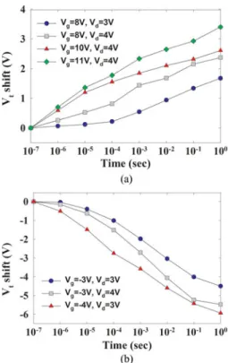
the so-called few-electron effect, which will be discussed fur-ther. The program characteristics as a function of pulse width for different operating conditions are shown in Fig. 4(a). Channel hot-electron injection and band-to-band hot-hole injection were
Fig. 2. (a) Top view scanning electron micrograph (SEM) image of the HfO2
nanocrystal device. (b) Planar-view HRTEM image of the nanoscaled trigate HfO2nanocrystal device.
Fig. 3. Id s–Vg scurves for the as-fabricated, programmed, and erased HfO2
nanocrystal memory devices.
employed for programming and erasing the memory, respec-tively. Both source and substrate terminals were biased at 0 V. The “Vtshift” is defined as the change in the threshold voltage
of a device between the written and the erased states. With Vd=
4 V and Vg= 11 V, a relatively high-speed (1 ms) programming
performance can be achieved with a memory window of about 2.2 V. Meanwhile, Fig. 4(b) demonstrates the erasing charac-teristics as a function of various operation voltages. Again, an excellent erasing speed of around 0.1 ms can be obtained.
The retention characteristics of the as-fabricated HfO2
nanocrystal memory devices at the different measuring tem-peratures (T = 25, 85, and 125◦C) are illustrated in Fig. 5. The
Fig. 4. (a) Program characteristics of HfO2nanocrystal memory devices with
different programming conditions. (b) Erasing characteristics of HfO2
nanocrys-tal memory devices with different erasing voltages.
Fig. 5. Retention characteristics of HfO2nanocrystal memory devices at T =
25, 85, and 125◦C.
retention time can be up to 108s for 17%, 41%, and 71% charge
losses at temperatures 25, 85, and 125 ◦C, respectively. We propose that the visible charge loss arises from the incomplete formation of well-isolated HfO2 nanocrystals after the 950◦C,
15 s RTA process. It is believed that a higher thermal budget can lead to better integrity of the nanocrystal formation. However, the largest allowable thermal budget is restricted by the dif-fusion of the dopants in the S/D regions. A higher temperature and longer period of annealing will result in extremely poor sub-threshold characteristics of the devices due to the punchthrough between the source and the drain. The endurance characteristics after 106 P/E cycles are also shown in Fig. 6. For operation of
our device, the programming and erasing conditions are Vg =
Fig. 6. Endurance characteristics of HfO2nanocrystal memory devices.
Neg-ligible degradation is found even after 105P/E cycles.
Fig. 7. Id s–Vg scurves of the 2-bit memory in a cell; forward read and reverse
read for programmed bit 1 and programmed bit 2.
11 V, Vd = 4 V for 0.1 ms and Vg = –4 V, Vg = 3 V for 0.1 ms,
respectively. Only a small narrowing of the memory window has been displayed, which is associated with a relatively small number of operation-induced trapped electrons being generated after cycling. Certainly, this result is intimately related to the use of ultrathin tunnel oxide and the minute amount of residual charges in the HfO2 nanocrystals after cycling. Fig. 7
demon-strates the feasibility of performing a 2-bit operation with our nanoscale HfO2 nanocrystal memories through a reverse read
scheme in a single cell. From the Ids– Vg scurves, it is clear that
we could employ forward and reverse reads to detect the infor-mation stored in the programmed bit 1 and bit 2, respectively. The read operation was achieved using a reverse read scheme. Table I summarizes the bias conditions for the 2-bit operation.
C. Different Length and Width Characteristics
Figs. 8 and 9 show how Vt shifts as a function of channel
length and width, respectively. The Vt shift clearly becomes
larger for devices with smaller channel widths (longer channel lengths) for a specific channel length (width). This tendency is consistent with that shown in [21]. Based on the numerical calculations, the authors demonstrated that this trend is mainly
TABLE I
OPERATINGPRINCIPLES ANDBIASCONDITIONSUTILIZEDDURING THE
OPERATION OF THEHfO2Nanocrystal Trigate Flash Memory Cell
Fig. 8. RT hysteresis characteristics of the fabricated devices for various chan-nel lengths. The inset shows the carrier mobiles with various chanchan-nel lengths.
Fig. 9. RT hysteresis characteristics of the fabricated devices with various channel widths. The inset shows the carrier mobiles with various channel widths.
caused by the presence of bottleneck regions that dominate the entire conductance in the ultranarrow channel once the charge is programmed into the nanocrystals. In the wide channel, the current can flow through the wide and low-potential region. By contrast, in the ultranarrow channel, the current path is com-pletely blocked in the bottleneck region, where one dot covers almost the entire channel bottleneck effect. Moreover, the aver-age potential in the ultranarrow channel is higher than that in the wide channel because of the effects of nanocrystals on the side surfaces. These effects are the origin of the larger Vt shift
in the ultranarrow devices.
Fig. 10. Read-disturbance characteristics of the HfO2 nanocrystal memory
devices.
Fig. 11. Drain current versus gate voltage characteristic for the few-electron effect.
D. Disturbance
Fig. 10 demonstrates the read-disturbance-induced erase-state threshold voltage instability under several operating con-ditions. For a 2-bit operation, the applied bit-line voltage in a reverse-read scheme must be sufficiently large (>1.5 V) to be able to “read through” the trapped charge in the neighbor-ing bit. The read-disturb effect is the result of two factors: the word line and the bit line. The word-line voltage during read-ing may enhance RT drift in the neighborread-ing bit [22]. On the other hand, a relatively large read bit-line voltage may cause unwanted channel hot-electron injection and, subsequently, re-sult in a significant threshold voltage shift of the neighboring bit. In our measurements, the gate and drain biases were applied and the source was grounded. The results demonstrate clearly that almost no read disturbance occurred in our memory devices under a low-voltage reading (Vg= 1.5 V; Vd = 1–2.5 V). E. Few-Electron Effect
First, we studied the drain current versus gate voltage char-acteristic, i.e., Id–Vg, of the memory devices at RT. The Id–Vg
characteristics of the HfO2 nanocrystal memories clearly show
the occurrence of the few-electron effect. In particular, in Fig. 11, the continuous curve corresponds to the Id–Vg measurement,
performed on a written device, when the gate bias is slowly swept down from 3 to −2 V. For this characteristic, abrupt peaks on the current are observed, corresponding to the sub-sequent discharging of few electrons from an HfO2
Fig. 12. Drain current versus gate voltage characteristic at low temperature (40 K) for swept time delay of 0.1 s.
performed with a fast voltage sweep on the same device after programming under various conditions. In this case, no dis-charging event occurs during the measurement. Moreover, we note that the continuous curve abruptly jumps from one dashed line to the other. Note that simultaneous injection/emission of electrons from different HfO2 dots is improbable because the
dots have a large size distribution in our devices. As reported in [23], the threshold voltage shift Vth is that induced by one
electron trapped in an HfO2dot. Based on this thesis, the
thresh-old voltage shift induced by only one electron trapped in one HfO2 dot, hereafter named δVth, in a device with W = L =
50 nm, is about 15 mV. Note that this value is of the same or-der of magnitude as the average experimental threshold voltage shift, which can be extracted from Fig. 11. Fig. 12 shows the
Id–Vg curve of the 106 P/E cycles for the stressed and
writ-ten memory devices at low temperature (40◦K), and the gate bias is slowly swept for a swept time delay of 0.1 s. The Id–Vg
characteristics of the HfO2 nanocrystal memories also clearly
show the occurrence of few-electron effect. From these charac-teristics, abrupt peaks in the current are observed more clearly, corresponding to the subsequent discharging of a few electrons from the HfO2nanocrystal. We use a normalized Id–Vgcurve to
fit them, and find that they still have the same order of magnitude of almost 15 mV.
IV. CONCLUSION
In this paper, we proposed a novel, simple, reproducible, and reliable technique for preparation of 50-nm-high-density HfO2 nanocrystals using spinodal decomposition of hafnium
silicate on SOI and achieved nanocrystal memories with char-acteristics including large memory windows, high program-ming/erasing speed, long retention time, and good endurance. The few-electron phenomenon at 40◦K was clearly observed. Discontinuities appear that corresponding to the discharging of a few electrons from HfO2 nanocrystals.
REFERENCES
[1] The International Technology Roadmap for Semiconductors. San Jose, CA: Semiconductor Industry Association, 2001, pp. 27–28. Available: http://www.itrs.net/reports.html
[2] P. Xuan, M. She, B. Harteneck, A. Liddle, J. Bokor, and T.-J. King, “FinFET SONOS flash memory for embedded applications,” in Proc.
IEDM Tech. Dig., 2003, pp. 609–613.
[3] T. Sugizaki, M. Kobayashi, M. Ishidao, H. Minakata, M. Yamaguchi, Y. Tamura, Y. Sugiyama, T. Nakanishi, and H. Tanaka, “Novel multi-bit SONOS type flash memory using a high-k charge trapping layer,” in Proc.
VLSI Symp. Technol. Dig. Tech. Papers, 2003, pp. 27–28.
[4] Blauwe, M. L. Ostraat, J. W. De, M. L. Green, L. D. Bell, M. L. Brongersma, J. Casperson, R. C. Flagan, and H. A. Atwater, “Synthesis and characterization of aerosol silicon nanocrystal nonvolatile floating-gate memory devices,” Appl. Phys. Lett., vol. 79, pp. 433–435, 2001. [5] T. Sugizaki, M. Kobayashi, H. Minakata, M. Yamaguchi, Y. Tamura,
Y. Sugiyama, H. Tanaka, T. Nakanishi, and Y. Nara, “New 2-bit/Tr MONOS type flash memory using Al2O3 as charge trapping layer,” in
Proc. IEEE Non-Volatile Semicond. Memory Workshop, Feb. 2003, pp. 60–
61.
[6] R. Ohba, N. Sugiyama, K. Uchida, J. Koga, and A. Toriumi, “Nonvolatile Si quantum memory with self-aligned doubly stacked dots,” IEEE Trans.
Electron Devices, vol. 49, no. 8, pp. 1392–1398, Aug. 2002.
[7] R. Muralidhar, R. F. Steimle, M. Sadd, R. Rao, C. T. Swift, E. J. Prinz, J. Yater, L. Grieve, K. Harber, B. Hradsky, S. Straub, B. Acred, W. Paul-son, W. Chen, L. Parker, S. G. H. AnderPaul-son, M. Rossow, T. Merchant, M. Paransky, T. Huynh, D. Hadad, Ko-Min Chang, and B. E. White Jr., “A 6 V embedded 90 nm Silicon nanocrystal nonvolatile memory,” in Proc.
IEDM Tech. Dig., 2003, pp. 601–605.
[8] T. Baron, B. Pellissier, L. Perniola, F. Mazen, J. M. Hartmann, and G. Pol-land, “Chemical vapor deposition of Ge nanocrystals on SiO2,” Appl.
Phys. Lett., vol. 83, pp. 1444–1446, 2003.
[9] Q. Wan, C. L. Lin, W. L. Liu, and T. H. Wang, “Structural and electrical characteristics of Ge nanoclusters embedded in Al2O3 gate dielectric,”
Appl. Phys. Lett., vol. 82, pp. 4708–4710, 2003.
[10] C. Lee, A. Gorur-Seetharam, and E. C. Kan, “Operational and reliabil-ity comparison of discrete-storage nonvolatile memories: Advantages of single- and double-layer metal nanocrystals,” in Proc. IEDM Tech. Dig., 2003, pp. 557–561.
[11] M. Takata, S. Kondoh, T. Sakaguchi, H. Choi, J-C. Shim, H. Kurino, and M. Koyanagi, “New non-volatile memory with extremely high density metal nano-dots,” in Proc. IEDM Tech. Dig., 2003, pp. 553–557. [12] M. F. Hung, Y. C. Wu, and Z. Y. Tang, “High performance gate-all-around
poly-Si nanowire with Si nanocrystals nonvolatile memory,” Appl. Phys.
Lett., vol. 98, pp. 162108-1–162108-3, 2011.
[13] L. C. Chen, Y. C. Wu, T. C. Lin, J. Y. Huang, M. F. Hung, J. H. Chen, and C. Y. Chang, “Poly-Si nanowire nonvolatile memory with nanocrys-tal indium–gallium–zinc–oxide charge-trapping layer,” IEEE Electron
Device Lett., vol. 31, no. 12, pp. 1407–1409, Dec. 2010.
[14] H. Zhou, B. Li, Z. Yang, N. Zhan, D. Yan, R. K. Lake, and J. Liu, “TiSi2nanocrystal metal oxide semiconductor field effect transistor
mem-ory,” IEEE Trans. Nanotechnol., vol. 10, no. 3, pp. 499–505, May 2011. [15] T. Sugizaki, M. Kobayashi, M. Ishidao, H. Minakata, M. Yamaguchi, Y. Tamura, Y. Sugiyama, T. Nakanishi, and H. Tanaka, “Novel multibit SONOS type flash memory using a high-κ charge trapping layer,” in Proc.
VLSI Symp. Technol. Dig. Tech. Papers, 2003, pp. 27–28.
[16] V. A. Gritsenko, K. A. Nasyrov, Yu. N. Novikov, A. L. Aseev, S. Y. Yoon, Jo-Won Lee, E.-H. Lee, and C. W. Kim, “A new low voltage fast SONOS memory with high-κ dielectric,” Solid State Electron., vol. 47, no. 10, pp. 1651–1656, 2003.
[17] Y.-H. Lin, C.-H. Chien, C.-T. Lin, C.-Y. Chang, and T.-F. Lei, “Novel two-bit HfO2 nanocrystal nonvolatile flash memory,” IEEE Trans. Electron
Device, vol. 53, no. 4, pp. 782–789, Apr. 2006.
[18] Y.-H. Lin, C.-H. Chien, C.-T. Lin, C.-Y. Chang, and T.-F. Lei, “High per-formance nonvolatile HfO2nanocrystal memory,” IEEE Electron Device
Lett., vol. 26, no. 3, pp. 154–156, Mar. 2005.
[19] W. J. Zhu, T.-P. Ma, T. Tamagawa, J. Kim, and Y. Di, “Current transport in metal/hafnium oxide /silicon structure,” IEEE Electron Device Lett., vol. 23, no. 2, pp. 97–99, Feb. 2002.
[20] S. Stemmer, Z. Chen, C. G. Levi, P. S. Lysaght, B. Foran, J. A. Gisby, and J. R. Taylor, “Application of metastable phase diagrams to silicate thin films for alternative gate dielectrics,” Jpn. J. Appl. Phys., vol. 42, pp. 3593–3597, 2003.
[21] M. Saitoh, E. Nagata, and T. Hiramoto, “Large memory window and long charge-retention time in ultranarrow-channel silicon floating dot mem-ory,” Appl. Phys. Lett., vol. 82, pp. 1787–1789, 2003.
[22] W. J. Tsai, C. C. Yeh, N. K. Zous, C. C. Liu, S. K. Cho, T. Wang, S. C. Pan, and C. Y. Lu, “Positive oxide charge-enhanced read disturb in a localized trapping storage flash memory cell,” IEEE Trans. Electron
Devices, vol. 51, no. 3, pp. 434–439, Mar. 2004.
[23] L. Guo, E. Leobandung, L. Zhuang, and S. Y. Chou, “Fabrication and char-acterization of RT silicon single electron memory,” J. Vac. Sci. Technol.
Yu-Hsien Lin (S’04–M’07) was born in Yi-Lan, Tai-wan, on June 18, 1979. He received the B.S., M.S., and Ph.D. degrees in electronics engineering from National Chiao-Tung University, Hsinchu, Taiwan, in 2001, 2002, and 2006, respectively. His Ph.D. dis-sertation research was focused on engineering and physics of advanced memory devices, in particular, nanocrystal based.
From 2006 to 2010, he was a Principle Engi-neer with the Taiwan Semiconductor Manufacturing Company (TSMC), Hsinchu, Taiwan, where he was involved in research and design for N40/N20 process integration and device performance improvement. In 2011, he joined the Department of Electronic Engineering, National United University, Miaoli, Taiwan, where he is currently an Assistant Professor. His research interests include novel nonvolatile memory devices, high-κ dielectric materials for CMOS devices, and polySi thin film transistors.
Chao-Hsin Chien (M’04–A’05) was born in 1968. He received the B.S., M.S., and Ph.D. degrees in elec-tronics engineering from National Chiao-Tung Uni-versity, Hsinchu, Taiwan, in 1990, 1992, and 1997, respectively. His Ph.D. dissertation research was fo-cused on plasma-induced charging damage on deep-submicrometer devices with ultrathin gate oxides.
In 1999, he joined National Nano Device Labora-tory as an Associate Researcher. In 2005, he became a Faculty Member in the Department of Electronics En-gineering, in National Chiao-Tung University,where he is currently a Full Professor. His research interests and activities cover high-κ dielectric, novel nonvolatile memory devices, organic devices, and nanowire.