國 立 交 通 大 學
電子工程學系電子研究所
博 士 論 文
具多閘極之修正蕭基位障電晶體及
氮化鈦奈米晶粒記憶體之研究
A Study on the Modified Schottky Barrier (MSB)
FETs and TiN Nanocrystal Memories with
Multi-Gate Structure
研 究 生:盧 季 霈
指導教授:崔 秉 鉞
具多閘極之修正蕭基位障電晶體及
氮化鈦奈米晶粒記憶體之研究
A Study on the Modified Schottky Barrier (MSB) FETs and
TiN Nanocrystal Memories with Multi-Gate Structure
研 究 生
: 盧季霈 Student : Chi-Pei Lu
指導教授
: 崔秉鉞 Advisor : Bing-Yue Tsui
國立交通大學
電子工程學系 電子研究所
博士論文
A Dissertation
Submitted to Department of Electronics Engineering
and Institute of Electronics
College of Electrical & Computer Engineering
National Chiao Tung University
In Partial Fulfillment of the Requirements
for the Degree of
Doctor of Philosophy
in Electronics Engineering
September 2010
Hsinchu, Taiwan, Republic of China
具
具
具
具多閘極
多閘極
多閘極
多閘極之修正
之修正
之修正蕭基位障電晶體及
之修正
蕭基位障電晶體及
蕭基位障電晶體及
蕭基位障電晶體及
氮化鈦奈米晶粒記憶體之研究
氮化鈦奈米晶粒記憶體之研究
氮化鈦奈米晶粒記憶體之研究
氮化鈦奈米晶粒記憶體之研究
研究生
研究生
研究生
研究生:
:
:
:盧季霈
盧季霈
盧季霈
盧季霈
指導教授:
指導教授
指導教授
指導教授
:
:崔秉鉞
:
崔秉鉞
崔秉鉞
崔秉鉞
國立交通大學電子工程學系電子研究所
國立交通大學電子工程學系電子研究所
國立交通大學電子工程學系電子研究所
國立交通大學電子工程學系電子研究所
摘要
摘要
摘要
摘要
隨著製程技術的蓬勃發展,互補式金氧半電晶體和非揮發性記憶體不斷地成 功微縮。然而,若持續在這些元件上使用傳統式的平坦結構設計,一些不可避免 的問題將會愈來愈嚴重。因此,不僅在邏輯元件或是記憶體元件上,多閘極結構 都已經被提出來用以改善元件的表現。在多閘極金氧半電晶體上,一種在源汲極 接面設計上進行改良的修正蕭基位障源汲極接面電晶體已被提出來改善電晶體特 性,除了可以提高驅動電流、降低外部阻抗,並可以保有原先蕭基位障電晶體所 具備的優點,例如:增加短通道效應的免疫力及降低汲極引發能帶降低效應 (drain-induced barrier lowing)。但是,到目前為止,對於修正蕭基位障電晶體來 說,仍有許多富有價值性的深入分析需要被探討。在非揮發性記憶體上,浮動閘 的設計已經被預測將會改良至電荷侷限儲存(charge trapping)的結構設計,例如改 用金屬奈米晶粒。因此,如何將多閘極結構與金屬奈米晶粒的儲存結構設計整合 在一起,亦是非常有價值性的探討。在本論文中,吾人對於多閘極修正蕭基位障電晶體之分析和多閘極氮化鈦金屬奈米晶粒記憶體之製備與特性做了深入的探 討。 首先,利用測量元件的溫度效應,蕭基位障與修正蕭基位障電晶體的電流傳 導機制被探討,並發現傳導機制主要受到蕭基位障的高度與長度來決定,而這些 參數都會受到製程及外加電場的影響。在蕭基位障電晶體上,電流傳導在小閘極 偏壓下會是由熱放射(thermionic emission)或穿透(tunneling)機制來主宰,而當在 足夠大閘極偏壓下,將轉變由漂移擴散(drift-diffusion)機制主導。而在修正蕭基 位障電晶體上,因為在源汲極延伸區域(SDE)有非常薄且高濃度的接面來有效地 壓抑蕭基位障,因此,隨著閘極電壓增加,電流傳導機制會由熱放射至穿透轉變 再轉變成漂移擴散方式來變化,而這些傳導機制的轉換點亦可以有效地用來評估 修正蕭基位障接面形成的好壞。另外,這些轉換點通常發生在大於臨限電壓 1 V 左右的位置,代表在小閘極偏壓下,修正蕭基位障仍然存在並影響著電流傳導。 吾人並且提出了改良式外部負載方法用以萃取在修正蕭基位障電晶體上具有 電壓相依性的源極端入射電阻(source injection resistance)。利用此方法分析觀察
得到,在小偏壓下,此入射電阻隨(VGS-Vth-0.5VDS)增加,呈現指數等級下降,但 在大偏壓下,將會停止下降並飽和在其外部串聯阻抗之值。這表示了源極端的修 正蕭基位障會主宰著電流直到外加偏壓足夠大到完全壓抑此蕭基位障為止。而 且,不同的熱預算的影響亦可用此方法觀察,若元件具有不足的後離子植入矽化 物之(post-ITS)退火,在小偏壓下會有明顯較大的串聯阻抗。並且,此種方法亦可 有效地用來判定修正蕭基位障的效率。 並且,我們亦成功製作出使用了 P+高功函數多晶矽閘極和氧化鋁高介電常 數阻擋層之奈米尺度的三閘極氮化鈦奈米晶粒非揮發記憶體,並探討不同的電荷
侷限捕捉層設計之影響。首先,此元件具有大記憶窗口達到 5.2 伏特且具有很好 的耐久度表現。並且,對於不同厚度的氮化鈦沾濕層(wetting layer)、後續沉積退 火(post deposition annealing)的時間和不同的阻擋層厚度對於記憶特性的影響亦有 研究。此次製作出的氮化鈦奈米晶粒直徑皆小於三奈米,如此會導致強烈的庫倫 阻斷效應(Coulomb blockage effect)並影響寫入/抹除速度和保存能力(retention)。
並且,經過 103秒的偏壓後,很小的閘極電壓擾動(gate disturbance)與讀取偏壓擾 動(read disturbance)亦可以達成。 最後,在此奈米尺度三閘極氮化鈦奈米晶粒非揮發記憶體測量中,吾人在關 閉反向讀取(reverse read)狀態下的源極電流上發現到一種不尋常但有趣的電流調 變現象。經過不同的偏壓條件操作後,這個電流調變的現象可以回覆到原先的電 流等級,並可來回操縱,表現出含有兩種狀態的可再現電阻調變現象。另外,此 現象可與操作在開啟狀態下的非揮發記憶體特性合併展現出具有兩位元(dual-bit) 操作方式的可能性。而且,藉由更進一步地分析其電流組成、儲存能力表現、溫 度效應、元件尺寸效應(area effect) 和閘極疊層設計的影響後,吾人推測出一個可 能在局部電荷侷限捕捉層產生或阻斷導電細絲(conducting filaments)而引發此電流 調變現象的操作模型。 總而言之,利用變溫測量和我們提出的改良式外部負載方法,在修正蕭基源 汲極電晶體上與閘極偏壓相關的電流傳導機制與源極端入射電阻分別被探討分 析。多閘極氮化鈦奈米晶粒非揮發記憶體亦被實現並具有良好的特性可做為微縮 之參考,並且發現了一個可重複操作的關閉電流調變現象,以及討論了其可能發 生的原因。
A Study on the Modified Schottky Barrier (MSB)
FETs and TiN Nanocrystal Memories with
Multi-Gate Structure
Student: Chi-Pei Lu
Advisor: Dr. Bing-Yue Tsui
Department of Electronics Engineering & Institute of Electronics
National Chiao-Tung University
Abstract
As the technology of CMOS and nonvolatile memory continuously scale down, several unpreventable issues would be encountered on the classical planar device structure. Hence, multi-gate structure is provided to enhance the device performance either on the logic device or on the flash memory. For the multi-gate MOSFETs, modified Schottky barrier (MSB) source/drain junction are proposed to apply on the MOSFETs to improve the driving current and reserve the advantages of SB MOSFETs, such as the immunity of short channel effect and less drain-induced barrier lowing effect. However, some further analyses on the MSB MOSFETs are still required. For nonvolatile memory, the floating gate structure is projected to migrate to the charge trapping devices, such as the metal nanocrystal. Hence, the integration of metal nanocrystals and multi-gate structure is worthy to investigate. In this dissertation,
multi-gate modified Schottky barrier MOSFETs and multi-gate metal TiN nanocrystal memory are investigated.
The current transportation mechanisms of the SB and MSB source/drain MOSFETs are investigated firstly. By measuring the temperature effect, it reveals that the current transportation mechanism is mainly dominated by the length and height of SB, which depends on the processes and the external supplying electric-field. For SB MOSFETs, the current transportation mechanisms start from the tunneling or thermionic emission at low gate bias and eventually become to the drift-diffusion at sufficient high gate bias. For MSB MOSFETs, since the source-side SB is suppressed by the ultra-thin and highly doped SDE, the current transportation mechanism changes from the thermionic emission to tunneling and then to drift diffusion as the gate voltage increases. Moreover, the changing point of mechanism is a good indicator to evaluate the efficiency of MSB junction. In addition, the changing point of mechanism is around at VG-VTH = 1 V, indicating the MSB still exists at low gate bias condition.
Then, the modified external loading method is proposed to extract the bias-dependent source injection resistance of the MSB source/drain MOSFETs. The injection resistance is observed to exponential proportion to the (VGS-Vth-0.5VDS) at low electric field but saturates to the source/drain resistance of conventional MOSFET at sufficient high electric field, suggesting the source-side MSB would dominate the current flow until the external bias large enough to suppress the barrier. The effect of the thermal budget of MSB process on the source injection resistance can observe. Sample without sufficient post-ITS annealing exhibits much higher RSD at low bias
region. Moreover, this method also provides a good method to evaluate the efficiency of MSB junction.
The charge trapping layer engineered nano-scale tri-gate TiN nanocrystal memories with high-k Al2O3 blocking layer and high work function P+ gate electrode
are successfully fabricated and investigated. Large memory window equals to 5.2 V and good endurance performance are achieved. Memory characteristics of various samples with different TiN wetting layer thickness, post deposition annealing time, and blocking oxide thickness are also investigated. The TiN nanocrystals are smaller than 3 nm, which induces strong Coulomb blockade effect to influence the P/E speed and retention property. Furthermore, the gate disturbance and read disturbance are also measured with very small charge migrations after 103sec. stressing bias.
Finally, an abnormal but interesting current modulation is observed in the off-state source current at reverse read on the nano-scale tri-gate TiN nanocrystal memory. By different pulse bias conditions, this current modulation can switch back and forth, showing a reproducible resistive switching behavior with two different states. Possible dual-bit operation is demonstrated. From the further analyses on the current components, the retention properties, the temperature effect, the area effect, and the engineering of gate stacks, a possible switching model is supposed due to the generation and rupture of the conducting filaments in the local charge trapping layer.
To summarize, the current transportation mechanism and the bias dependent source injection resistance of the MSB MOSFETs are investigated by measuring the temperature effect and our provided modified external loading method, respectively. The multi-gate SAMOS-type TiN nanocrystal nonvolatile memories are realized and an interesting repeatable current modulation is demonstrated and the possible reason is discussed.
誌謝
誌謝
誌謝
誌謝
本論文的完成,首先要感謝我的指導教授 崔秉鉞博士。在我的研究所生涯 豬,感謝老師一直不眠不休地在研究、論文和實驗上給予學生充分且完善的指 導,讓學生獲益良多,並且當學生在研究中遇到困難時,給予適時的鼓勵與支 持。另外,老師嚴謹的研究態度與正直又親切的處世風範,更是讓學生受益匪 淺,並且亦積極鼓勵學生努力拓展國際視野,更是學生得以前往德國進行研究的 催化劑以及一大支持,謝謝老師。 其次我要感謝國家奈米實驗室以及交大奈米中心還有工研院電光所提供優良 的製程設備以及良善的管理使得實驗能夠順利進行,並特別感謝國家奈米實驗室 的劉正財、鄭旭君、薛富國與巫振榮先生等,在製程中提供許多寶貴的意見及熱 心的幫忙。另外,也要感謝奈米中心的陳明麗、黃月美與徐秀鑾小姐等,在實驗 上的幫忙。也要特別感謝工研院電光所的林哲歆、曾培哲、王慶鈞博士等在實驗 設計以及製程上的大力幫忙。諸位口試委員的細心指正與建議,特別表示感謝。 並且,也衷心的感謝奈米技術實驗室的成員們: 國龍、家彬、誌鋒、偉 豪、志民、修維、逸璿、智勛、立峰、宜澤、聖銘、永助、孟漢、明錡、佳蓉、 勻珮、振銘、振欽、玉仁、筱函、曉萱、雨蓁、正愷、孝瑜、瑞堯、俊凱、依 成、昆武勃學、子歆、智超等,也要感謝淳雅和所有幫助與關心過我的朋友以及 學長、同學們,有你們這些年的陪伴關心與大力支持,才讓我能夠克服研究低 潮,使我渡過漫長研究所生涯,順利完成論文。 最後,我要特別感謝我的父母 盧廷池先生與 魏麗華女士,從小全心全力栽 培,並且一路上都支持我、愛護我、相信我,讓我可以無後顧之憂的投入學業。 謹將這份榮耀獻給我的父母。Content
Abstract(Chinese) ...i
Abstract(English) ... iv
Content... viii
Table Captions ... xi
Figure Captions... xii
Chapter 1
Introduction...1
1.1 Scaling of CMOS Technology ...1
1.2 Multi-gate structure...3
1.3 Modified Schottky Barrier (MSB) Multi-gate FETs ...4
1.4 Multi-Gate nanocrystal memories (NCM)...6
1.4.1 Evolution of the planar nonvolatile memory...7
1.4.2 Multi-gate charge trapping Flash memory...11
1.5 Thesis Organization ...12
Chapter 2
Current Transportation Mechanisms of Schottky Barrier (SB)
MOSFETs and Modified Schottky Barrier (MSB) MOSFETs...25
2.1 Introduction...25
2.2 Devices Fabrication...27
2.2.2 Tri-Gate MOSFETs with p-MSB Source/Drain ...29
2.3 Results and Discussion...30
2.3.1 Basic Current-Voltage Characteristics...30
2.3.2 Fundamental Theory ...32 2.3.3 SB MOSFETs ...33 2.3.4 n-MSB MOSFETs...35 2.3.5 p-MSB MOSFETs...36 2.4 Conclusions...37
Chapter 3
Extraction of Bias-Dependent Source Injection Resistance of
Modified Schottky Barrier MOSFET...64
3.1 Introduction...64
3.2 Devices Fabrication...66
3.3 Modified External Loading Method (ELM)...68
3.3.1 The ELM on Conventional pn junction MOSFETs ...68
3.3.2 The Modify ELM on MSB MOSFETs...70
3.3.3 Selection of RLoad on Modify ELM ...72
3.3.4 Bias-Dependent Source Injection Resistance of MSB MOSFETs...73
3.4 Conclusions...74
Chapter 4
Nano-scale Multi-gate TiN Metal Nanocrystal Memory ...96
4.2 Devices Fabrication...99
4.3 Results and Discussion...101
4.3.1 Program/Erase Efficiency and Memory Window ...101
4.3.2 Retention Performance ...104
4.3.3 Retention Performance in Different P/E Conditions...106
4.3.4 Endurance and Disturbance Performance...107
4.4 Conclusions...108
Chapter 5
Abnormal Current Modulation in the Turn-off State of 1-T
Nano-Scale Multi-Gate Nanocrystal Memory ...130
5.1 Introduction...130
5.2 Devices Fabrication and Experiment ...132
5.3 Results and Discussion...132
5.3.1 Current Modulation and Switching Behavior in the Off-State ...132
5.3.2 Further Analyses on the Off-State Current Modulation ...134
5.3.3 Possible Switching Mechanism...138
5.3.4 Potential of Dual-Bit Operation ...140
5.4 Conclusions...141
Chapter 6
Conclusions and Further Recommendations ...159
6.1 Conclusions...159
Table Captions
Chapter 3
Table3.1 The important structure parameters of samples A-E. ………79
Chapter 4
Table4.1 Gate stacks conditions of samples A-D. ………115
Chapter 5
Figure Captions
Chapter 1
Fig.1-1 Schematic cross-section views of (a) planar MOSFET, and (b) planar UTB SOI FET. ………22 Fig.1-2 Schematic structures of the FinFETs on SOI substrate, (a) double-gate
FinFETs, and (b) tri-gate FinFETs. ……….23 Fig.1-3 Basic structure of (a) FG flash memory device, (b) SONOS flash
memory device, and (c) nanocrystal flash memory device. …………24
Chapter 2
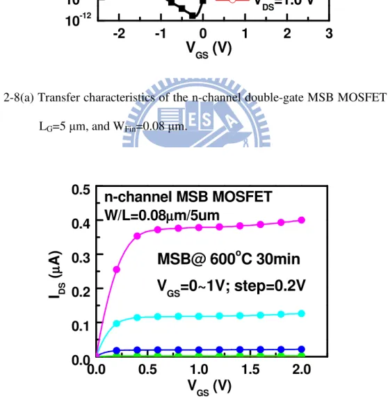
Fig.2-1 Process flow of the double-gate n-channel MSB MOSFETs. ……….43 Fig.2-2 Process flow of the tri-gate p-channel MSB MOSFETs. ………45 Fig.2-3(a) Transfer characteristics of n-channel double-gate SB MOSFET with
LG=5 µm, and WFin=0.08 µm. ………..46
Fig.2-3(b) Transfer characteristics of p-channel double-gate SB MOSFET with LG=5 µm, and WFin=0.08 µm. ………..46
Fig.2-4(a) Output characteristics of n-channel double-gate SB MOSFET with LG=5 µm, and WFin=0.08 µm. ………..47
Fig.2-4(b) Output characteristics of p-channel double-gate SB MOSFET with LG=5 µm and WFin=0.08 µm. ………...47
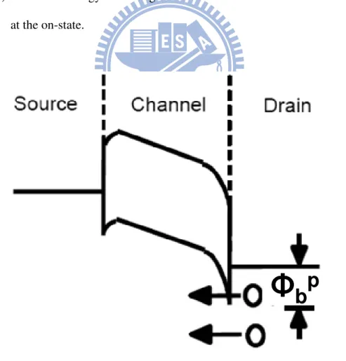
Fig.2-5(a) Schematic energy band diagram of the n-channel SB MOSFETs operates at the on-state. ………...48
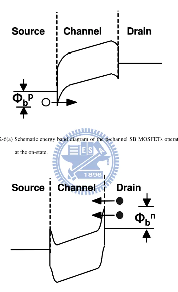
Fig.2-5(b) Schematic energy band diagram of the n-channel SB MOSFETs operates at the off-state. ………...48 Fig.2-6(a) Schematic energy band diagram of the p-channel SB MOSFETs operates at the on-state. ………...49 Fig.2-6(b) Schematic energy band diagram of the n-channel SB MOSFETs
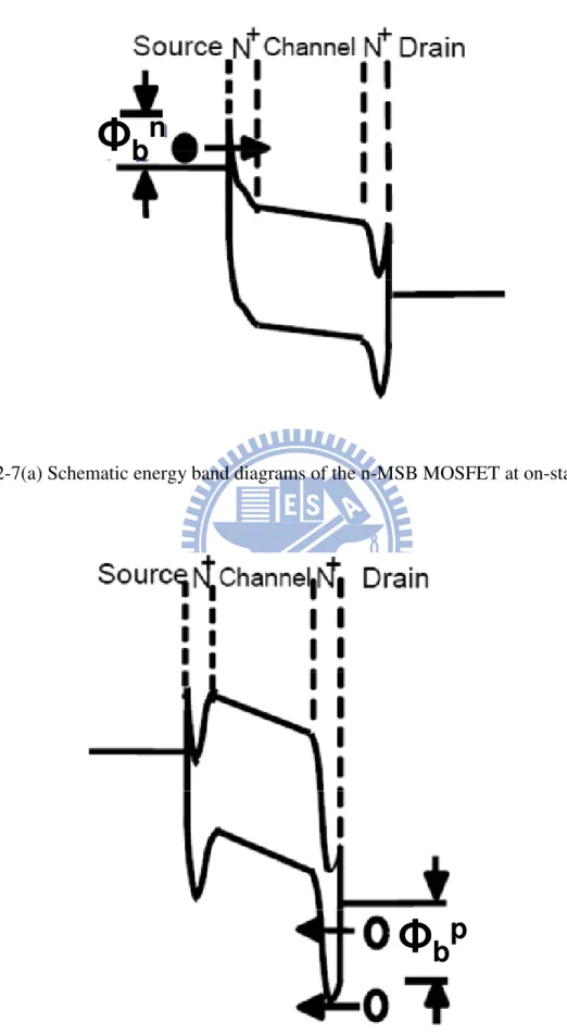
operates at the off-state. ………...49 Fig.2-7(a) Schematic energy band diagrams of the n-MSB MOSFET at
on-state. ……… 50 Fig.2-7(b) Schematic energy band diagrams of the n-MSB MOSFET at off-state. ……… 50 Fig.2-8(a) Transfer characteristics of the n-channel double-gate MSB MOSFET
with LG=5 µm, and WFin=0.08 µm. ……….51
Fig.2-8(b) Output characteristics of the n-channel double-gate MSB MOSFET with LG=5 µm, and WFin=0.08 µm. ……….51
Fig.2-9(a) Schematic energy band diagrams of the p-MSB MOSFET at on-state. ……… 52 Fig.2-9(b) Schematic energy band diagrams of the p-MSB MOSFET at
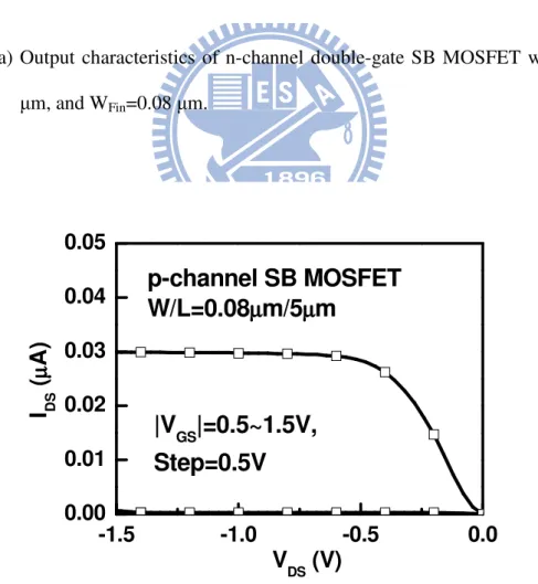
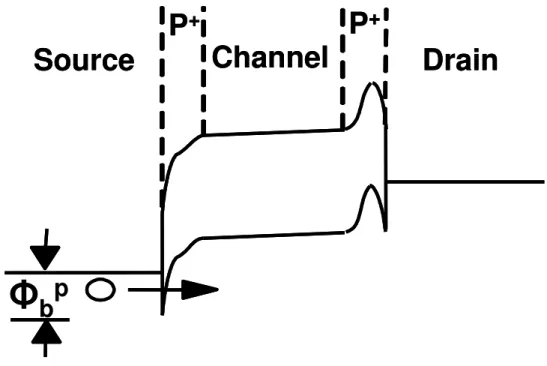
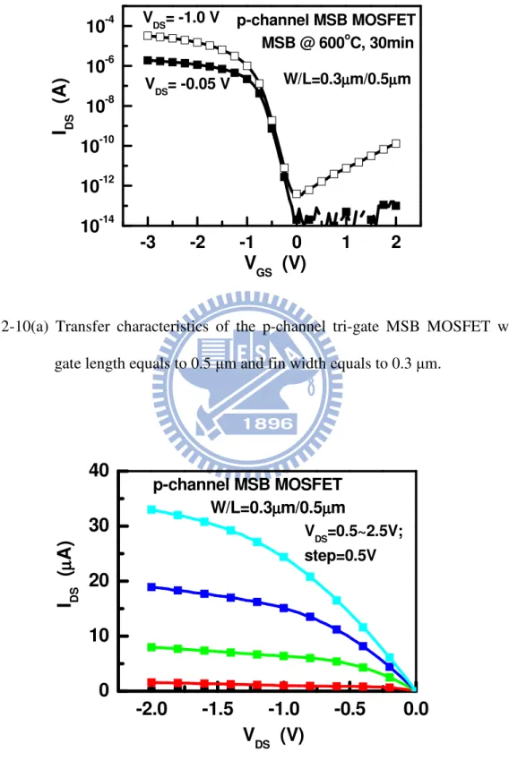
off-state. ……… 52 Fig.2-10(a) Transfer characteristics of the p-channel tri-gate MSB MOSFET with
gate length equals to 0.5 µm and fin width equals to 0.3 µm. ……….53 Fig.2-10(b) Output characteristics of the p-channel tri-gate MSB MOSFET with gate length equals to 0.5 µm and fin width equals to 0.3 µm. ……….53 Fig.2-11 Transfer characteristics of the n-channel SB MOSFET with gate length equals to 5 µm and fin width equals to 80 nm. ………54 Fig.2-11 Transfer characteristics of the n-channel SB MOSFET shown in Fig.
11 in linear scale with VDS=0.05 V. ………55
Fig.2-12(a) Transfer characteristics of the n-channel SB MOSFET shown in Fig. 11 in linear scale with VDS=1.0 V. ………..…55
Fig.2-13 Transfer characteristics of the p-channel SB MOSFET with gate length equals to 5 µm and fin width equals to 80 nm. ………56 Fig.2-14(a) Transfer characteristics of the p-channel SB MOSFET shown in Fig. 13 in linear scale with VDS= -0.05 V. ………...57
Fig.2-14(b) Transfer characteristics of the p-channel SB MOSFET shown in Fig. 13 in linear scale with VDS= -1.0 V. ………..………...57
Fig.2-15 Transfer characteristics of the n-channel MSB MOSFET with gate length equals to 5 µm and fin width equals to 80 nm. ……….58 Fig.2-16(a) Transfer characteristics of the n-channel MSB MOSFET shown in Fig. 15 in linear scale with VDS= 0.05 V. ………...59
Fig.2-16(b) Transfer characteristics of the n-channel MSB MOSFET shown in Fig. 15 in linear scale with VDS= 1.0 V. ………...59
Fig.2-17 Transfer characteristics of the n-channel MSB MOSFET in linear scale with VDS=0.05 V and the post-ITS annealing at 600 ºC for 30 sec or for
30 min. ………...60
Fig.2-18 Transfer characteristics of the n-channel MSB MOSFET with the post-ITS annealing at 600 ºC for 30 sec or for 30 min. ………...61 Fig.2-19 Transfer characteristics of the p-channel MSB MOSFET with gate length equals to 0.5 µm and fin width equals to 0.3 µm. ……….62 Fig.2-20(a) Transfer characteristics of the p-channel MSB MOSFET shown in Fig. 19 in linear scale with VDS= -0.05 V. ………..63
19 in linear scale with VDS= -1.0 V. ………....64
Chapter 3
Fig.3-1 Main Process flow of n-channel double-gate MSB MOSFET with HfAlO gate dielectric layer. ………...80 Fig.3-2(a) Transfer characteristics of the n-channel MSB MOSFET with HfAlO gate dielectric layer and two different post-ITS annealing. ………….81 Fig.3-2(b) Output characteristics of the n-channel MSB MOSFET with HfAlO gate dielectric layer and two different post-ITS annealing. ………….81 Fig.3-3(a) Transfer characteristics of the n-channel MSB MOSFET with SiO2
gate dielectric layer and two different post-ITS annealing. …………82 Fig.3-3(b) Output characteristics of the n-channel MSB MOSFET with SiO2 gate
dielectric layer and two different post-ITS annealing. ………82 Fig.3-4 The Effective circuit diagram of the external loading method. An
external load resistor with suitable range of impendence is connected to the source terminal. ………...83 Fig.3-5 The 1/IDS versus RL plot of the conventional pn source/drain MOSFET
with SiO2 gate dielectric layer (sample E). ……….84
Fig.3-6 The -RL0 versus 1/(VGS-VTH-0.5VDS) plot of sample E. The inset displays the illustration of device structure. ………85 Fig.3-7 The 1/IDS versus RL plot of MSB source/drain MOSFET with SiO2 gate
dielectric layer (sample C). ………..86 Fig.3-8 The -RL0 versus 1/(VGS-VTH-0.5VDS) plot of sample C. The inset displays the illustration of device structure. ………87 Fig.3-9 Extracted RT as a function of (VGS-VTH-0.5VDS) of the MSB MOSFET
SiO2 gate dielectric layer and two different post-ITS annealing (sample
C and sample D). ……….88 Fig.3-10(a) The -RL0 versus 1/(VGS-VTH-0.5VDS) plot of MSB MOSFET with HfAlO gate dielectric layer (sample A). ………..89 Fig.3-10(b) The -RL0 versus 1/(VGS-VTH-0.5VDS) plot of MSB MOSFET with HfAlO gate dielectric layer (sample A). ………..89 Fig.3-11 Extracted RT as a function of (VGS-VTH-0.5VDS) of the MSB MOSFET with HfAlO gate dielectric layer and two different post-ITS annealing (sample A and sample B). ……….…..90 Fig.3-12 The 1/IDS versus RL plot of MSB source/drain MOSFET with HfAlO
gate dielectric layer (sample A). Smaller loads are used to extract the
RT. ……….………...91
Fig.3-13 The 1/IDS versus RL plot of MSB source/drain MOSFET with HfAlO gate dielectric layer (sample A). Larger loads are used to extract the
RT. ………92
Fig.3-14 The -RL0 versus 1/(VGS-VTH-0.5VDS) plot of MSB MOSFET with SiO2
gate dielectric layer (sample C) at VDS = 0.05 V to 0.3 V. …………..93
Fig.3-15(a) Extracted series resistance of sample C as a function of (VGS-VTH
-0.5VDS) in the linear scale. ……….…..94 Fig.3-15(b) Extracted series resistance of sample C as a function of (VGS-VTH
-0.5VDS) in the log scale. ……….……..94 Fig.3-16(a) Extracted series resistance of sample D as a function of (VGS-VTH
-0.5VDS) in the linear scale. ……….…..96 Fig.3-16(b) Extracted series resistance of sample D as a function of (VGS-VTH
Chapter 4
Fig.4-1 Main Process flow of n-channel double-gate MSB MOSFET with HfAlO gate dielectric layer. ………...116 Fig.4-2(a) High-resolution X-TEM images of the fabricated MuGFET TiN nanocrystal memory with gate length of 80 nm. ………...117 Fig.4-2(b) High-resolution X-TEM images of the fabricated MuGFET TiN
nanocrystal memory with fin width of 50 nm. ………...117 Fig.4-3(a) High-resolution X-TEM images of sample A. Nanocrystals with diameter around 3 nm were embedded by Al2O3. ……….118
Fig.4-3(b) High-resolution X-TEM images of sample B. Nanocrystals with diameter around 1-2 nm were embedded by Al2O3. ………..118
Fig.4-4 Transfer characteristics of sample A after various P/E bias for 0.1 sec. ……….119 Fig.4-5(a) Programming speeds of samples A-D with same pulse bias at +10 V
and different pulse width. ………..120 Fig.4-5(b) Erasing speeds of samples A-D with same pulse bias at -10 V and
different pulse width. ………..………...120 Fig.4-6 The memory window of sample A-D after various P/E bias for 0.1 sec. The P/E operations utilized Fowler-Nordheim tunneling, and both source and drain terminals were grounded during the biasing pulse..121 Fig.4-7(a) Programming speeds of sample A with various pulse biases and pulse widths. ………...122 Fig.4-7(b) Erasing speeds of sample A with various pulse biases and pulse
widths. ………...122 Fig.4-8 Retention characteristics of trigate TiN nanocrystal memory devices of
samples A-B at room temperature (T = 25 °C) and high temperature (T
= 85 °C). ……….…...123 Fig.4-9 Retention properties of sample C in two different P/E conditions but similar initial memory window. ………...124 Fig.4-10 Simple energy band diagrams in the retention condition after (a)
moderate erasing bias or (b) stronger erasing bias. ………...125 Fig.4-11 Endurance characteristics of samples A and B. The P/E bias conditions
are ±9 V, 0.1 sec for sample A and ±12 V, 0.1 sec for sample B. …126 Fig.4-12(a) Transfer characteristics after the first and the 104th P/E cycle operations
of sample A. ………...127 Fig.4-12(b) Transfer characteristics after the first and the 104th P/E cycle operations
of sample B. ………...127 Fig.4-13 Gate disturbance characteristics of sample A in four different states. ………..128 Fig.4-14 Read disturbance of sample A in erase state for 103 sec stressing bias. ………....129
Chapter 5
Fig.5-1(a) Transfer characteristics after applying for the first pulsing at VG/VD =
+6/+6 V. ………...146 Fig.5-1(b) Transfer characteristics after applying for the second pulsing at VG/VD= -6/+6 V. The off-state current modulation shows in the RR
mode. ………...146 Fig.5-1(c) Transfer characteristics after applying for the third pulsing at VG/VD=
+6/+6 V. Reproducible switching phenomenon shows in the turn-off state. ………...147 Fig.5-2 Retention performance in FR and RR of sample A after pulsing bias at VG/VD= -6/+6 V and 25 °C. ………...148
Fig.5-3 Retention performance at HRS and LRS of sample A at 25 °C and 85 °C. ………...149 Fig.5-4(a) Current components of sample A after pulsing at VG/VD= -6/+6 V.
Main gate leakage current comes from the drain electrode. ………..150 Fig.5-4(b) Current components of sample A after pulsing at VG/VD= +6/+6 V.
Gate leakage current mainly depends on the potential difference. …150 Fig.5-5 The off-state current in sample A with different chuck temperature. No temperature dependence of the off-state current is observed at higher negative gate bias. ………...151 Fig.5-6(a) Current components of sample A after pulsing at VG/VD= -6/+6 V with
grounding the source and drain electrodes. ………...152 Fig.5-6(b) Current components of sample A after pulsing at VG/VD= +6/+6 V
with grounding the source and drain electrodes. ………...152 Fig.5-7 The electrical-bias-induced resistive switching phenomenon in sample A-C. The property of the charge trapping layer controls the HRS current and the thickness of the blocking layer dominates the magnitude of the LRS current. ………..153 Fig.5-8(a) Output characteristics of sample A with the VG biases from -6 V to +6
V. Impact ionization and punchthrough effects induce abrupt current. ………...154 Fig.5-8(b) Gate leakage current of sample A with the VG biases from -6 V to +6 V.
Large gate current is sensed as the VG/VD = -6/+6 V. ………...154
Fig.5-9 Transfer characteristics of sample A with the VD bais from 2.9 V to 3.4
V. When the VD=3.2 V, outstanding subthreshold swing equals to 2.5
mV/decade is obtained owing to the impact ionization and punchthrough effects induced abrupt current. ………...155 Fig.5-10 The area dependence of the current modulation in sample A. Currents of HRS and LRS with different gate length are shown. No clear difference between the HRS and LRS as the gate length larger than 0.16 µm. ………...156 Fig.5-11(a) The schematic illustrations of the possible switching mechanism after VG/VD = -6/+6 V (HRS). Smaller source current is sensed. ……….157
Fig.5-11(b) The schematic illustrations of the possible switching mechanism after VG/VD = +6/+6 V (LRS). Larger source current is sensed. ………...157
Fig.5-12 Potential of dual-bit operation in the nanoscale multi-gate nanocrystal memory cell. It is achieved by resistive switching in the off-state and NCM operation in the on-state. ……….158
Chapter 1
Introduction
1.1 Scaling of CMOS Technology
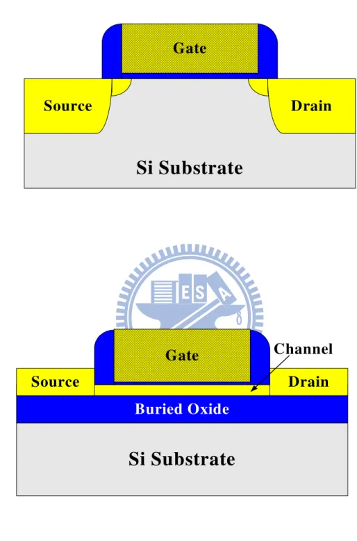
In the past four decades, the rapid growth in electronics industry mainly bases on the successful scaling of each technology generation, providing better device performance, faster circuit operation speed, lower power consumption, and lower production cost. This scaling trend mostly follows the Moore’s law, which is an empirical observation by Gordon Moore in 1965 that the transistor density of integrated circuit doubles and the feature size of device are scaled by a factor of 0.7 every eighteen months [1]. Nowadays, the 32 nm generation node has been achieved. However, from the recently prediction of International Technology Roadmap for Semiconductor (ITRS), to obtain higher driving current and lower leakage current in the conventional planar bulk CMOS, some critical challenges would be encountered in the further downscaling. These challenges mainly originate from the gate leakage, source-drain leakage, and junction leakage. Figure 1-1(a) presents the schematic cross-sectional view of the typical planar MOSFET. To get good gate controllability and suppress the short-channel effect (SCE), the gate-to-channel capacitance (Cgc)
must be maximized. It can be achieved by thinning the thickness of SiO2 gate
dielectric. However, the extremely large gate leakage current due to the direct tunneling would stop the SiO2 scaling. This problem can be solved by using the high
dielectric constant (high-k) material as the gate dielectric layer to replace the SiO2 thin
film, since thicker film can be utilized to achieve the same Cgc. Today, the equivalent
oxide thickness (EOT) is around 0.95 nm for high-performance (HP) logic applications [2]. Additionally, high channel doping and shallow junction are also required to suppress source-drain leakage current to maintain tolerable short-channel effect. However, the doping concentration is too high (~1019 cm-3) for the continued scaling device, resulting in degraded carrier mobility, low driving current, high junction leakage current induced by band-to-band tunneling, and severe gate-induced drain leakage (GIDL) [1-3]. Therefore, from the forecast in ITRS 2009, non-classical CMOS structures with better electrostatic controllability will be implemented in the future, such as ultra-thin body (UTB) MOSFET [4-5] and multi-gate FET (MuGFET) [6-8].
Comparing to the structure of the planar bulk CMOS, UTB MOSFET, the silicon-on-insulator (SOI) substrate has an extremely thin silicon layer for the channel and a buried SiO2 layer for isolation. It can effectively control the potential through
the whole channel and suppress source-drain leakage current and short-channel effect without requiring the highly dosed punch-through implantation. Hence, UTB MOSFET with low-doped channel obtains larger carrier mobility, enhanced current drive, and better immunity to short channel effect. It has been predicted that the UTB structure would be applied as the technology node below than 27 nm for high performance logic applications [2]. The schematic structure of the UTB SOI MOSFET is shown in Figure 1-1(b). To suppress the issues originate from the SCE and to achieve better turn-off characteristic, thinner Si layer is required as scaling of the gate length. However, some critical challenges will be encountered for the further scaling. Normally, from the experimental observation, the Si thickness is demanded
approximately one third of the gate length for the UTB SOI MOSFET, indicating the required Si thickness thinner than 10nm as the gate length shorter than 30 nm [9]. However, as the Si thickness thinner than 10nm, quantum confinement effect arises and it causes an increasing of threshold voltage as compare to a thick-body device [10]. Moreover, the variation in the body thickness is another concern. Hence, controllability of the threshold voltage and the thickness of ultra-thin body are the most critical issues for the UTB SOI MOSFET. Hence, owing to the aforementioned reasons, the limitation of UTB structure is forecasted around 22 nm node for the CMOS applications. Then, multi-gate FETs (MuGFET) have been thought as a possible solution for the further scaling as the technology node beyond 22 nm [2].
1.2 Multi-gate structure
MuGFETs such as FinFET [6-7,10-11], gate-all-around (GAA) FET [12-14] include two or more than two gates, exhibiting better gate controllability to fully deplete Si channel and show significant reduction of short channel effect as compare to the UTB SOI MOSFET. Therefore, multi-gate structure is expected to replace the UTB structure in the future and become the most possible solution for the further scaling. Moreover, high channel doping is not required to suppress S/D leakage current and hence higher mobility can be obtained. Additionally, the FinFETs include a double-gate or tri-gate structure with relative similar processes and structure, except the hard-mask layer on the top of Si fin. When the hard-mask layer stays on the top of Si fin, double-gate FinFET is realized, implying two sidewall channel will turn-on in the on-state; when the hard-mask layer is removed on the top of Si fin, tri-gate FinFET is accomplished, indicating two sidewall channel and one top channel will
turn-on in the on-state. Figures 1-2(a) and 1-2(b) present the schematic structures of the double-gate and the tri-gate FinFETs. Moreover, FinFETs have better driving current and lower off-current with compatible processes and similar layout design to that of the classical bulk CMOS. Furthermore, the effective channel width is increased by the double-gate structure or tri-gate structure. For example, the effective width in the double-gate FinFET is double of the fin-height. Then, the effective width in the tri-gate FinFET is double of the fin-height plus the fin-width. Hence, the effective driving current can be enhanced by using this three-dimensional structure.
1.3 Modified Schottky Barrier (MSB) Multi-gate FETs
Following the future scaling steps, as the multi-gate structure employing in the device, the fin width gets much narrower, thus much higher series resistance would exist outside of the channel since lacking of deep source/drain (S/D) regions to achieve lower enough resistance by forming metal silicide [15]. Hence, to effectively minimize parasitic source/drain resistance (RSD) and increase the driving current,
some techniques have been presented, such as the raised source/drain [16] and low barrier silicide S/D [17-20]. The raised S/D realizes by the selective epitaxial growth (SEG) on the Si channel can effective thicken the Si fin and obtain lower RSD.
However, applying this technique on the MuGFETs has high complexity and it may induce some failures during the process, such as agglomeration, facet, or bridging effect [11]. The low resistive S/D silicide is fabricated by the thermal reaction of the metal and the Si layers at S/D regions, which would produce Schottky barriers (SB) at the interface of the silicide and the Si-channel and lower the external RSD. Moreover,
SB MOSFETs have been proposed with highly suitable for future nano-scale devices because it offers benefits such as easy processing, low thermal budget, and small external resistance of S/D [17-20]. Hence, devices with low Schottky barrier height silicides, such as PtSi for p-MOSFET [17, 18], and ErSi2-x [17, 19], YbSi2-x [20], and
DySi2-x [18] for n-MOSFET have already been demonstrated. However, the SB
MOSFETs still have some drawbacks. First, using complementary S/D silicides for nFET and pFET requires a dual-silicide process, inducing much more complexity and large modification for mass production. Furthermore, owing to the existence of the SB in the turn-on state, smaller on-state driving current (Ion) is exhibited than that of the
conventional pn junction MOSFETs. The existed SB not only affects the driving capability but also degrades the performance of the sub-threshold swing [21]. Moreover, the problem of high turn-off current (Ioff) of SB MOSFETs comes from the
carrier injection at the drain side is the other drawback [22]. Furthermore, in all of the present silicides, the extracted SB height are around 0.15 eV – 0.25 eV, which is not low enough to outperform the performance of the convention CMOS with highly doped S/D junction because the requirement of the SB height is smaller than 0.1 eV [23]. Therefore, by using the metal S/D to lower external S/D series resistance in the MuGFET needs another solution to overcome the aforementioned issues.
Recently, modified Schottky barrier (MSB) MOSFETs have been proposed to improve the driving current and reserve the advantages of SB MOSFETs such as better short channel effect and less drain-induced-barrier-lowering [10, 11]. The MSB junction is a Schottky junction with a very thin but high doping concentration layer located at silicide/Si-channel interface which not only drastically improves the driving capability by reducing and thinning the SB at source junction but also can significantly suppress the off-state leakage current due to the thick SB at drain
junction. Hence, am-bipolar current-voltage characteristics can be significantly improved by using the MSB technology.
The MSB junction can be accomplished by either implantation-to-silicide (ITS) method or dopant segregation (DS) method [10, 11]. For the ITS method, dopants are implanted to the pre-formed S/D silicide regions follows a low temperature annealing to migrate the dopants to the silicide/Si interface to form the ultrathin and steep MSB junction. As contrary, for the DS method, the dopants are implanted before silicidation. During silicidation, the dopants are segregated at the silicide/Si interface and construct the MSB junction. Hence, the formation of MSB junction only requires low temperature process which is suitable for the integration of high-k/metal gate stacks. Moreover, the carrier injection velocity enhancement associated with the velocity overshoot is observed in the dopant-segregated MOSFETs [24]. Besides, several literatures have been devoted to evaluate the efficiency of the MSB junction. Recently, M. Zhang et al. reported that the effective Schottky barrier height can be reduced to about 0.1 eV at high gate bias [25]. However, the gate bias dependence of the series resistance in the MSB MOSFETs and the current transport mechanisms of the MSB MOSFETs have not been reported.
1.4 Multi-Gate nanocrystal memories (NCM)
As the scaling trend of the CMOS logic device has been forecasted that the planar structure may be replaced by the three-dimensional structure, i.e. multi-gate. The nonvolatile memory has been considered to modify its planar structure to the three-dimensional architecture since some challenges would be encountered. Moreover, because the multi-gate structure offers some advantages such as better gate
controllability and higher gate coupling ratio, multi-gate structure seems to be a candidate for the future application of nonvolatile memory. However, some inevitable issues would rise as scaling, which is mainly originated from the storage material and it is suspected to change another applicable material as the new storage node. Hence, firstly, we should focus on what happened in the past of the nonvolatile memory and what it is predicted to change.
1.4.1 Evolution of the planar nonvolatile memory
In the past years, the market of the nonvolatile memory has huge growth and it makes the Flash memories as one of the fastest growing semiconductor products. Lots of commercial products need the Flash memory, mostly relating to the mobile digital consumer application, such as MP3, PDA, digital cameras and so on. The current state-of-the-art for the flash memory is based on the floating gate (FG) technology which has nearly 100% market share [26]. The FG flash stands out owing to its highly compatibility with the CMOS technology and good scalability to achieve extremely high density. In 1967, D. Kahng and S. M Sze invented the first floating gate non-volatile memory (NVM) at Bell Lab [27]. Till today, various kinds of floating gate memories have been proposed and the process technology progressed rapidly. Figure 1-3(a) shows the schematic cross-section structure of the basic floating gate flash memory. The device structure is mainly based on the MOSFET with a modified gate stacks, including a control gate (CG) and a floating gate separated by a dielectric layer. The storage node is the isolated floating gate. Floating gate NVM has the advantages of large memory window, high program/erase (P/E) speed, and good reliability. Moreover, for the commercial applications, the FG NVM can satisfy the requirements of high density, low power consumption, smaller form factor, and lower system cost
[26]. Hence, flash memory becomes one of the fastest growing semiconductor technologies and provides hundreds of portable electronic products in last decade. However, the International Technology Roadmap for Semiconductors (ITRS) forecasts that the scaling limitation of the conventional floating gate memories is around 25 nm node [28] and some challenges would encounter in the near future. The main issue is un-scalable tunneling oxide thickness. For allowing charge transfer to the FG at reasonable voltage, the tunneling oxide layer must be thin enough but for maintaining acceptable retention performance in read-mode or off-state, the tunneling oxide layer have to be thick enough to avoid charge loss. Therefore, higher operation voltages are needed for present FG technology and the thickness of tunneling oxide layer is predicted to keep at 6-7 nm and it is very hard to decrease [28]. Moreover, since the floating gate is a conductive material, the stored charges will leak easily if the tunneling oxide is damaged during operations. The gate coupling ratio (GCR) is required to larger than 0.6. It can be enlarged by thinning the thickness of inter-poly dielectric (IPD) layer, however, for the data retention requirement, the thickness of IPD decreases slowly as scaling. Moreover, the short channel effect becomes more critical as scaling. The increasing floating gate to floating gate coupling effect is another urgent issue for the continually closing floating gate memory cell. Therefore, the FG technology is projected to migrate to the charge trapping devices with discrete traps for charge storage, such as SONOS (Silicon/ Oxide/ Nitride/ Oxide/ Silicon) and nanocrystal (NC) structures [28].
Since the cross-talk between thin charge-trapping layers is negligible, the largest advantage of the charge-trapping devices is the immune of the floating gate to floating gate cross-talk effect. Moreover, the charge-trapping devices also enable to utilize thinner gate stacks to enhance gate controllability and suppress short channel effect
[29]. Figure 1-3(b) shows the schematic cross-section structure of the SONOS-type flash memory. The storage node is the silicon nitride layer. Theoretically, when the CG is biased positively, electrons would tunnel through the tunneling oxide layer and be trapped by the deep level in the silicon nitride layer. As contrary, when the CG is biased negatively, the trapped electrons would be ejected from the nitride layer and back into the channel. Therefore, the SONOS-type memory which stores charges in the discrete trap node of silicon nitride layer exhibits improved retention performance so that the tunneling oxide thickness can be reduced to increase the P/E speed and to decrease the operation voltage [30-31]. Besides, some advanced SONOS memories such as bandgap engineered SONOS (BE-SONOS) and TANOS (TaN/ Al2O3/
Nitride/ Oxide/ Silicon) have demonstrated high P/E speed and attracted much attention for applying in the future NVM [32, 33]. BE-SONOS use triple ultra-thin layers of ONO as the tunnel dielectric layer. Each ultra-thin layer is around 1-2 nm thick. Because the smaller energy barrier of Si3N4 layer to hole, the injection
efficiency of hole in the erasing-mode can be enhanced. Moreover, the effective thickness of the tunneling dielectric layer still thick enough to prevent the escaping of the trapped electrons in the read-mode or off-state. The retention performance still performs well. TANOS uses metal gate electrode and high-k blocking dielectric layer to prevent back-side gate injection when erasing and obtained fast erasing speed. Additionally, the usage of high-k dielectric can enhance the electric field at tunneling oxide layer and improve the GCR to enhance the programming efficiency. Unfortunately, the erase saturation [34] and unwanted migration of stored charges in the nitride layer [35] are the major drawbacks and can be observed in all SONOS-type memories. Therefore, nanocrystal memories have been thought as promising candidates for the future NVM application.
Nanocrystal memory which uses various materials as the storage node such as Si, Ge, HfO2, Pt, Ag, Au, Ni and TiN has been proposed and became another possible
solution for the future NVM applications [36-44]. Figure 1-3(c) shows the schematic cross-section structure of the nanocrystal flash memory. Owing to each nanocrystal is theoretically isolated by surrounding dielectric, nanocrystal memory have better charge storage ability than SONOS-type memory. The lateral migration of storage charges can be theoretically removed and the crosstalk behavior between the bits of source-side and drain-side would not be observed. Therefore, it may show better performance of the multi-bit operation [36]. Moreover, thinner tunneling oxide can be used to improve P/E speed and reduced P/E operation voltage without degrading the retention performance. In 2002, Liu et al. proposed the design principle and fabrication process of metal nanocrystal memories [36-37]. The self-assembled nanocrystal can be formed easily by deposition a thin metal layer followed by a rapid thermal annealing (RTA). Besides, metal nanocrystals have more work function engineering ability, higher density of state around Fermi-level, stronger coupling to the Si-channel, and better size scalability than the semiconductor nanocrystals have. Although lots of literatures were proposed to provide various techniques to form nanocrystals, one of the main challenges of nanocrystal memory is the storage node property which means the nanocrystal quality. She et al. has proposed in 2003 that the optimized size of Ge nanocrystal is 5 nm with concerning about the effect of Coulomb blockade and quantum confinement [38]. Therefore, how to formation nanocrystals with high density, constant size, and uniform distribution [39-41] is required to be concerned, especially when the device getting smaller and smaller. Some variation of the nanocrystal’s property in different device would induce unstable storage data in these nanocrystal memories.
1.4.2 Multi-gate charge trapping Flash memory
The multi-gate structure is not only a possible solution for the CMOS logic device but also very attractive for the future application of memory devices, especially for the nonvolatile memory. For the non-volatile memory (NVM), it has thicker gate dielectric, implying worse channel controllability. Hence, multi-gate structure, such as FinFET structure, can be utilized to suppress the short channel effect and improve the gate coupling ratio by wrapping sidewall FG. In 2003, Xuan et al. have proposed the first FinFET SONOS flash memories with excellent program/erase characteristics and good reliability performance [45]. Recently, multi-gate field effect transistors (MuGFETs) were predicted as one of the most potential solution for the NAND Flash beyond the 25 nm node, and various SONOS-type and nanocrystal memories have been fabricated with multi-gate structure [28]. It has been reported that the multi-gate memory cell can achieve excellent short-channel effect controllability, high driving current, low leakage current, good programming inhibition, and large numbers of nanocrystals in one cell of nanocrystal memory [42-50]. Furthermore, the potential of a floating fin-type body is modulated in the multi-gate structure, differently from that in the single gate structure, exhibiting a longer charge retention time [43]. Additionally, multi-level operation [46] and dual-bit operation [47] in the FinFET SONOS-type flash memories are also achieved. Moreover, some technologies which utilized in the planar flash memory to improve the property are also applicable on the multi-gate FinFET Flash memories. Cho et al. has proposed that using high-k inter-poly dielectric layer as blocking layer can enlarge gate coupling ratio and then enhance programming/erasing efficiency [48]. In 2007, Hsu et al. presented the FinFET bandgap engineered BE-SONOS flash memory with better retention and
erase speed than that of FinFET SONOS [49]. The FinFET WN nanocrystals flash memory with Al2O3 high-k blocking layer and trapping layer engineering by adding
extra nitride layer has been investigated. Owing to the additional trap sites in Si3N4,
the memory window and the retention performance are improved [42]. Hence, multi-gate structure provides a selection to reduce the scaling limitation and it is an important candidate for further scaling of NVM. Therefore, both in the CMOS and NVM, this kind of three-dimensional structure displays extremely large possibility and scaling capability for the future applied technology.
1.5 Thesis Organization
In this dissertation, we mainly focus on the some possible solutions for the multi-gate MOSFET and multi-multi-gate flash memory. In the first part, the influence by the existed Schottky barriers on a multi-gate MOSFET and a novel extraction method of the series resistance in MSB S/D MOSFET are also described. In the second part, a nano-scale multi-gate nanocrystal memory has been demonstrated as a promising candidate for the NAND flash memory application.
In the first chapter of this dissertation, some overviews of the CMOS revolution and its challenges will be mentioned. Non-planar device structure, such as multi-gate structure, is highly considered for the future application on the logic CMOS transistors and the Flash memory. The advantage and the shortcoming for using multi-gate are also described. For CMOS devices, multi-multi-gate structure and metal S/D are forecasted for the further scaling. Modified Schottky barrier S/D junction is one possible solution for the future S/D engineering. For flash memory, multi-gate
structure is also a candidate. Moreover, the possible enhancement of the charge storage element and its revolution are also reviewed.
In chapter 2, current transport mechanisms of SB S/D MOSFETs and MSB S/D MOSFETs are investigated by measuring the temperature effect on current-voltage characteristics. The current transport mechanism varied while different gate voltage was biased. Moreover, the SB height would impact the transport mechanism largely in different gate bias conditions.
In chapter 3, we provide a novel method for extracting gate voltage dependent source injection resistance of MSB MOSFETs. The relationship between the injection resistance and the gate bias will be discussed. Furthermore, this method provides a good indicator to evaluate the efficiency of the MSB junction directly.
In chapter 4, the fabrication and the electrical characteristics of a nano-scale n-channel tri-gate TiN nanocrystal non-volatile memory has been demonstrated. The Al2O3 high-k blocking layer and the P+ high work function gate electrode were used
to obtain low operation voltage and suppress the back-side injection effect, respectively. TiN nanocrystals were formed by annealing the TiN/Al2O3
nano-laminates which were deposited by an atomic layer deposition system. Moreover, the charge-trapping layer has engineered with different TiN wetting layer thickness, post deposition annealing time, and blocking oxide thickness. The size of the nanocrystal affects the performance largely. Moreover, the memory characteristics and the reliability performance of these samples have been demonstrated.
In chapter 5, we demonstrate an interesting resistive switching phenomenon in the turn-off state in the naon-scale multi-gate TiN nanocrystal memory. This electric-bias-induced reproducible change of reverse read current are observed after pulsing at the conditions of CHE and BTBHH, normally utilizing for the NOR flash operations.
This abnormal leakage current will be investigated and possible mechanism will be discussed.
Finally, in chapter 6, we will give some important conclusions. Moreover, some further works which are worthy for further study will be suggested.
References
[1] L. Risch, “Pushing CMOS beyond the roadmap,” Solid-state Electron., vol. 50, no. 4, pp. 527-535, 2006.
[2] Process Integration, Devices and Structures in International Technology Roadmap for Semiconductors 2009 edition, pp. 1-10, 2009.
[3] L. Chang, Y.-K. Choi, J. Kedzierski, N. Lindert, P. Xuan, J. Bokor, C. Hu, and T.-J. King, “Moore’s Law Lives on,” IEEE Circuits and Devices Mag., vol. 19, no. 1, pp. 35-42, 2003.
[4] Y.-K. Choi, K. Asano, N. Lindert, V. Subramanian, T.-J. King, J. Bokor, and C. Hu, “Ultrathin-Body SOI MOSFET for Deep-Sub-Tenth Micron Era,” IEEE
Electron Devices Lett., vol. 21, no. 5, pp. 254-255, 2000.
[5] K. Uchida, J. Koga, R. Ohba, T. Numata, and S. Takagi, “Experimental Evidences of Quantum-Mechanical Effects on Low-field Mobility, Gate-channel Capacitance, and Threshold Voltage of Ultrathin Body SO1 MOSFETs,” in
IEDM Tech. Dig., 2001, pp. 633-636.
[6] B. Yu, L. Chang, S. Ahmed, H. Wang, S. Bell, C.-Y. Yang, C. Tabery, C. Ho, Q. Xiang, T.-J. King, J. Bokor, C. Hu, M.-R. Lin, and D. Kyser, “FinFET scaling to 10 nm gate length,” in IEDM Tech. Dig., 2002, pp. 251-254.
[7] N. Lindert, L. Chang, Y.-K. Choi, E. H. Anderson, W.-C. Lee, T.-J. King, J. Bokor, and C. Hu,“Sub-60-nm Quasi-Planar FinFETs Fabricated Using a Simplified Process,” IEEE Electron Devices Lett., vol. 22, no. 10, pp. 487-489, 2001.
[8] R. H. Yuan, A. Ourmazd, and K. Lee, “Scaling the Si MOSFET: from bulk to SOI to bulk,” IEEE Trans. Electron Devices, vol. 39, no. 7, pp. 1704-1710, 1992.
[9] J. Chen, R. Solomon, T.-Y. Chan, P. K. KO, and C. Hu, “Threshold Voltage and C-V Characteristics of SO1 MOSFET’s Related to Si Film Thickness Variation on SIMOX Wafers,” IEEE Trans. Electron Devices, vol. 39, no. 10, pp. 2346-2353, 1992.
[10] B.-Y. Tsui, C.-P. Lin, “A novel 25-nm modified schottky-barrier FinFET with high performance,” IEEE Electron Device Lett., vol. 25, no. 6, pp. 430-432, 2004. [11] A. Kaneko, A. Yagishita, K. Yahashi, T. Kubota, M. Omura, K. Matsuo, I.
Mizushima, K. Okano, H. Kawasaki, T. Izumida, T. Kanemura, N. Aoki, A. Kinoshita, J. Koga, S. Inaba, K. Ishimaru, Y. Toyoshima, H. Ishiuchi, K. Suguro, K. Eguchi, Y. Tsunashima, “High-Performance FinFET with Dopant-Segregated Schottky Source/Drain,” in IEDM Tech. Dig., 2006, pp. 893-896.
[12] K. H. Yeo, S. D. Suk, M. Li, Y. Yeoh, K. H. Cho, K.-H. Hong, S. Yun, M. S. Lee, N. Cho, K. Lee, D. Hwang, B. Park, D.-W. Kim, D. Park, and B.-I. Ryu, “Gate-All-Around (GAA) Twin Silicon Nanowire MOSFET (TSNWFET) with 15 nm Length Gate and 4 nm Radius Nanowires,” in IEDM Tech. Dig., 2006, pp. 539-542.
[13] N. Singh, A. Agarwal, L. K. Bera, T. Y. Liow, R. Yang, S. C. Rustagi, C. H. Tung, R. Kumar, G. Q. Lo, N. Balasubramanian, and D.-L. Kwong, “High-Performance Fully Depleted Silicon Nanowire (Diameter ≤ 5 nm) Gate-All-Around CMOS Devices,” IEEE Electron Device Lett., vol. 27, no. 5, pp. 383-386, 2006.
[14] J. W. Peng, S. J. Lee, G. C. A. Liang, N. Singh, S. Y. Zhu, G. Q. Lo, and D. L. Kwong, “Improved carrier injection in gate-all-around Schottky barrier silicon nanowire field-effect transistors,” App. Phys. Lett., vol. 93, no. 7, p. 073503, 2008.
[15] A. Dixit, A. Kottantharayil, N. Collaert, M. Goodwin, M. Jurczak, and K. De Meyer, “Analysis of the parasitic S/D Resistance in Multiple-Gate FETs,” IEEE
Trans. Electron Devices, vol. 52, no. 6, pp. 1132-1140, 2005.
[16] J. Kedzierski, M. Ieong, E. Nowak, T. S. Kanarsky, Y. Zhang, R. Roy, D. Boyd, D. Fried, and H.-S. P. Wong, “Extension and source/drain design for high-performance FinFET devices,” IEEE Trans. Electron Devices, vol. 50, no. 4, pp. 952-958, 2003.
[17] J. Kedziersk, P. Xuan, E. H. Andersonf, J. Bokor, T.-J. King, C. Hu, “Complementary silicide source/drain thin-body MOSFETs for the 20nm gate length regime,” in IEDM Tech. Dig., 2000, pp. 57-60.
[18] S. Zhu, H. Y. Yu, S. J. Whang, J. H. Chen, C. Shen, C. Zhu, S. J. Lee, M. F. Li, D. S. H. Chan, W. J. Yoo, A. Du, C. H. Tung, J. Singh, A. Chin, and D. L. Kwong, “Schottky-Barrier S/D MOSFETs With High-K Gate Dielectrics and Metal-Gate Electrode,” IEEE Electron Device Lett., vol. 25, no. 5, pp. 268-270, 2004.
[19] M. Jang, Y.Kim, J. Shin, S. Lee, and K. Park, “ A 50-nm-gate-length erbium-silicided n-type Schottky barrier metal-oxide-semiconductor field-effect transistor,” App. Phys. Lett., vol. 84, no. 5, pp. 741-743, 2004.
[20] R. T. P. Lee, A. E.-J. Lim, K.-M. Tan, T.-Y. Liow, G.-Q. Lo, G. S. Samudra, D. Z. Chi, and Y.-C. Yeo, “N-channel FinFETs With 25-nm Gate Length and Schottky-Barrier Source and Drain Featuring Ytterbium Silicide.” IEEE Electron
Device Lett., vol. 28, no. 2, pp. 164-167, 2004.
[21] J. Knoch, M. Zhang, Q. T. Zhao, St. Lenk, S. Mantl, and J. Appenzeller, “Effective Schottky barrier lowering in silicon-on-insulator Schottky-barrier metal-oxide-semiconductor field-effect transistors using dopant segregation,”
App. Phys. Lett., vol. 87, no. 26, p. 263505, 2005.
[22] J. Knoch and J. Appenzeller, “Impact of the channel thickness on the performance of Schottky barrier metal–oxide–semiconductor field-effect transistors,” Appl. Phys. Lett., vol. 81, no. 16, pp. 3082-3084, 2002.
[23] S. Xiong, T.-J. King, and J. Bokor, “A Comparison Study of Symmetric Ultrathin-Body Double-Gate Devices With Metal Source/Drain and Doped Source/Drain,” IEEE Trans. Electron Devices, vol. 52, no. 8, pp. 1859-1867, 2005.
[24] A. Kinoshita, T. Kinoshita, Y. Nishi, K. Uchida, S. Toriyama, R. Hasumi, and J. Koga, “Comprehensive Study on Injection Velocity Enhancement in Dopant-Segregated Schottky MOSFETs,” in IEDM Tech. Dig., 2006, pp. 79-82.
[25] M. Zhang, J. Knoch, Q.T. Zhao, A. Fox, St. Lenk, and S. Mantl, “Low temperature measurements of Schottky-barrier SOI-MOSFETs with dopant segregation,” Electronics Letters, vol. 41, no. 19, pp. 1085-1086, 2005.
[26] R. Bez, and A. Pirovano, “Non-volatile memory technologies: emerging concepts and new materials,” Materials Science in Semiconductor Processing, vol. 7, no. 4-6, pp. 349-355, 2004.
[27] D. Kahng and S. M Sze, “A floating gate and its application to memory devices,”
IEEE Trans. Electron Devices, vol. 14, no. 9, p. 629, 1967.
[28] Process Integration, Devices and Structures in International Technology Roadmap for Semiconductors 2009 edition, pp. 13-20, 2009.
[29] J. Fu, N. Singh, K. D. Buddharaju, S. H. G. Teo, C. Shen, Y. Jiang, C. X. Zhu, M. B. Yu, G. Q. Lo, N. Balasubramanian, D. L. Kwong, E. Gnani, and G. Baccarani, “Si-Nanowire Based Gate-All-Around Nonvolatile SONOS Memory Cell,” IEEE
[30] M. H. White, D. A. Adams, and J. Bu, “On the go with SONOS,” IEEE Circuits
and Devices Magazine, vol. 16, no. 4, pp. 22-31, 2000.
[31] J. Bu, and M. H. White, “Effects of Two-step High Temperature Deuterium Anneals on SONOS Non-volatile Memory Devices,” IEEE Electron Device Lett., vol. 22, no. 1, pp. 17-19, 2001.
[32] H. T. Luo, S. Y. Wang, E. K. Lai, Y. H. Shih, S. C. Lai, L. W. Yang, K. C. Chen, J. Ku, K. Y. Hsieh, R. Liu, and C. Y. Lu, “BE-SONOS: A Bandgap Engineered SONOS with Excellent Performance and Reliability,” in IEDM Tech. Dig., 2005, pp. 547-550.
[33] C.-H. Lee, J. Choi, C. Kang, Y. Shin, J.-S. Lee, J. Sel, J. Sim, S. Jeon, B.-I. Choe, D. Bae, K. Park, and K. Kim, “Multi-Level NAND Flash Memory with 63 nm-node TANOS (Si-Oxide-SiN-Al2O3-TaN) Cell Structure,” in VLSI Symp. Tech.
Dig., 2006, pp. 21-22.
[34] Gowrishankar L. Chindalore, Member, IEEE, Craig T. Swift, and David Burnett,
Member, IEEE, “A New Combination–Erase Technique for Erasing Nitride Based (SONOS) Nonvolatile Memories,” IEEE Electron Device Lett., vol. 24, no. 4, pp. 257-259, 2003.
[35] T. Sugizaki, M. Kohayashi, M. Ishidao, H. Minakata, M. Yamaguchi, Y. Tamura, Y. Sugiyama, T. Nakanishi, and H. Tanaka, “Novel Multi-bit SONOS Type Flash Memory Using a Highk Charge Trapping Layer,” in VLSI Symp. Tech.
Dig., 2003, pp. 27-28.
[36] Z. Liu, C. Lee, V. Narayanan, G. Pei, and E. C. Kan, “Metal Nanocrystal Memories—Part I: Device Design and Fabrication,” IEEE Trans. Electron
Devices, vol. 49, no. 9, pp. 1606-1613, 2002.
Memories—Part II: electrical characteristics,” IEEE Trans. Electron Devices, vol. 49, no. 9, pp. 1614-1622, 2002.
[38] M. She, and T.-J. King, “Impact of Crystal Size and Tunnel Dielectric on Semiconductor Nanocrystal Memory Performance,” IEEE Trans. Electron
Devices, vol. 50, no. 9, pp. 1934-1940, 2003.
[39] J. J. Lee, and D. -L. Kwong, “Metal Nanocrystal Memory With High-k Tunneling Barrier for Improved Data Retention,” IEEE Trans. Electron Devices, vol.52, no. 4, pp. 507-511, 2005.
[40] S. Maikap, P. J. Tzeng, H. Y. Lee, C. C. Wang, T. C. Tien, L. S. Lee, and M. -J. Tsai, “Physical and electrical characteristics of atomic layer deposited TiN nanocrystal memory capacitors,” Appl. Phys. Lett., vol. 91, no. 4, p. 043114, 2007.
[41] S. Choi, S. S. Kim, M. Chang, H. Hwang, S. Jeon, C Kim, “Highly thermally stable TiN nanocrystals as charge trapping sites for nonvolatile memory device applications,” Appl. Phys. Lett., vol. 86, no.12, p. 123110, 2005.
[42] Y. J. Ahn, J. -D. Choe, J. J. Lee, D. Choi, E. S. Cho, B. Y. Choi, S. -H. Lee, S. K. Sung, C. -H. Lee, S. H. Cheong, D. K. Lee, S. B. Kim, D. Park and B. I. Ryu, “Trap Layer Engineered FinFET NAND Flash with Enhanced Memory Window,” in VLSI Symp. Tech. Dig., 2006, pp. 88-89.
[43] K. Yanagidaira, M. Saitoh, and T. Hiramoto, “Enhancement of Charge Storage Performance in Double-Gate Silicon Nanocrystal Memories With Ultrathin Body Structure,” IEEE Electron Devices Lett., vol. 26, no. 7, pp. 473-475, 2005.
[44] C.-P. Lu, C.-K. Luo, B.-Y. Tsui, C.-H. Lin, P.-J. Tzeng, C.-C. Wang, and M.-J. Tsai, “Nanoscale Multigate TiN Metal Nanocrystal Memory Using High-k Blocking Dielectric and High-Work-Function Gate Electrode Integrated on
Silcon-on-Insulator Substrate,” Jap. J. Appl. Phys., vol. 48, p. 04C059, 2009. [45] P. Xuan, M. She, B. Harteneck, A. Liddle, J. Bokor, and T.-J. King, “FinFET
SONOS Flash Memory for Embedded Applications,” in IEDM Tech. Dig., 2003, pp. 609-612.
[46] M. Specht, U. Dorda, L. Dreeskornfeld, J. Kretz, F. Hofmann, M. Städele, R. J. Luyken, W. Rösner, H. Reisinger, E. Landgraf, T. Schulz, J. Hartwich, R. Kömmling, and L. Risch, “20 nm tri-gate SONOS memory cells with multi-level operation,” in IEDM Tech. Dig., 2004, pp. 1083-1085.
[47] M. Specht, R. Kömmling, F. Hofmann, V. Klandzievski, L. Dreeskornfeld, W. Weber, J. Kretz, E. Landgraf, T. Schulz, J. Hartwich, W. Rösner, M. Städele, R. J. Luyken, H. Reisinger, A. Graham, E. Hartmann, and L. Risch, “Novel Dual Bit Tri-Gate Charge Trapping Memory Devices,” IEEE Electron Devices Lett., vol. 25, no. 12, pp. 810-812, 2004.
[48] E. S. Cho, C.-H. Lee, T.-Y. Kim, S.-K. Sung, B. K. Cho, C. Lee, H. J. Cho, Y. Roh, D. Park, K. Kim and B.-I. Ryu, “Hf-silicate Inter-Poly Dielectric Technology for sub 70nm Body Tied FinFET Flash Memory,” in VLSI Symp.
Tech. Dig., 2005, pp.208-209.
[49] T.-H. Hsu, H. T. Lue, Y.-C. King, J.-Y. Hsieh, E.-K. Lai, K.-Y. Hsieh, R. Liu, and C.-Y. Lu, “A High-Performance Body-Tied FinFET Bandgap Engineered SONOS (BE-SONOS) for NAND-Type Flash Memory,” IEEE Electron Devices
Lett., vol. 28, no. 5, pp. 443-445, 2007.
[50] F. Hofmann, M. Specht, U. Dorda, R. Kömmling, L. Dreskorndeld, J. Kretz, M. Städele, W. Rösner, and L. Risch, “NVM based on FinFET device structures,”
(a)
Si Substrate
Gate
Source
Drain
(b)
Si Substrate
Gate
Buried Oxide
Source
Drain
Channel
Fig. 1-1 Schematic cross-section views of (a) planar MOSFET, and (b) planar UTB SOI FET.
(a)
(b)
Fig. 1-2 Schematic structures of the FinFETs on SOI substrate, (a) double-gate FinFETs, and (b) tri-gate FinFETs.