國 立 交 通 大 學
電子工程學系 電子研究所碩士班
碩 士 論 文
具環繞閘極與多重奈米通道之複晶矽薄膜電晶體研究
Study on the Gate-All-Around Poly-Si TFTs with Multiple
Nanowire Channels
研 究 生:涂仕煒
Shih-Wei Tu
指導教授:鄭晃忠 博士
Dr. Huang-Chung Cheng
具環繞閘極與多重奈米通道之複晶矽薄膜電晶體研究
Study on the Gate-All-Around Poly-Si TFTs with Multiple
Nanowire Channels
研 究 生:涂仕煒
Student : Shih-Wei Tu
指導教授:鄭晃忠 教授
Advisor : Dr. Huang-Chung Cheng
國立交通大學
電子工程學系 電子研究所碩士班
碩士論文
A Thesis
Submitted to Department of Electronics Engineering & Institute of Electronics
College of Electrical and Computer Engineering
National Chiao Tung University
In Partial Fulfillment of the Requirements for the Degree of Master
in
Electronic Engineering
June, 2008
Hsinchu, Taiwan, Republic of China
具環繞閘極與多重奈米通道之
複晶矽薄膜電晶體研究
研究生:涂仕煒 指導教授:鄭晃忠 博士
國立交通大學
電子工程學系 電子研究所碩士班
摘要
複晶矽薄膜電晶體被廣泛的應用於主動式矩陣平面顯示器的開關元件,
而 為了要更進一步把複晶矽薄膜電晶體應用在系統面板和三維立體積體電路上,複 晶矽薄膜電晶體的尺寸勢必要縮小來提高積體電路的密度和操作速度。然而當傳 統複晶矽薄膜電晶體的尺寸縮小時,由於在通道中的晶界缺陷和薄膜電晶體的浮 體結構(Floating Body),元件會發生一些非理想的效應,像是臨界電壓下降、汲 極誘導能障下降和紐結效應(Kink Effect)。在這篇論文裡我們提出了新穎具環繞 閘極與多重奈米通道之複晶矽薄膜電晶體來改善元件的性能。 在第二章,我們利用一種簡單且低成本的方式來製作元件。我們利用間隙壁技術(Spacer Technique)來製作奈米通道而不用先進的微影技術。並利用蝕刻犧牲 氧化層來讓奈米通道懸空能被閘極完全包覆形成環繞閘極結構。由掃描式電子顯 微鏡和穿透式電子顯微鏡的觀察發現閘極與閘極氧化層的包覆非常的均勻。製作 出的具環繞閘極與多重奈米通道之複晶矽薄膜電晶體和傳統的元件比較起來有 相當良好的電特性。在電晶體導通時,我們的元件有較低的臨界電壓(由 2.31 到 1.31 V)、較小的汲極誘導能障下降(由 0.29 到 0.04 V/V)、較陡峭的次臨界擺幅(由 0.64 到 0.37 V/decade)、較低的紐結電流、較高的導通電流(由 3.81×10⁻⁵到 4.17×10⁻⁵ A)與載子移動率(由 26 到 33 cm2/V-s)。當電晶體關閉,我們的元件在低 閘極電壓時有較低的漏電流,但在高閘極電壓時有較高的漏電流,這是由於我們 的元件有較高的閘極電場。 在第三章,我們更進一步的研究具環繞閘極與多重奈米通道之複晶矽薄膜電 晶體的特性。在氨電漿鈍化效應上,我們的元件能更有效的被氨電漿鈍化。此外, 我們比較了具環繞閘極與多重奈米通道、具斜邊閘極與多重奈米通道與傳統閘極 三種不同結構的複晶矽薄膜電晶體。在這些結構中,具環繞閘極與奈米通道的複 晶矽薄膜電晶體展現了最好的特性。另外我們也比較不同尺寸的元件,和傳統的 複晶矽薄膜電晶體相比,我們的元件也能有效抑制短通道效應和窄通道效應。另 一方面,我們應用間隙壁奈米通道的尖端成功製作場發射元件。
Study on the Gate-All-Around Poly-Si TFTs With Multiple
Nanowire Channels
Student: Shih-Wei Tu Advisor: Dr. Huang-Chung Cheng
Department of Electronics Engineering & Institute of Electronics
National Chiao Tung University
ABSTRACT
Poly-Si thin film transistors (TFTs) have been widely used as switching elements in active matrix displays. Further, for the applications on system-on-panel (SOP) and three-dimension integrated circuits (3-D ICs), scaled-down poly-Si TFTs are needed for higher integrated density and faster speed. However, there are some undesired effects in conventional scaled-down poly-Si TFTs such as threshold voltage (Vth) roll-off, drain-induced barrier lowering (DIBL), and kink effect which are caused from the grain boundary defects and the floating body in channel region. In this thesis, novel gate-all-around poly-Si TFTs with multiple nanowire channels (GAA-MNC TFTs) were proposed to improve the device performance.
In the chapter 2, a simple and low-cost method was used in fabricating the GAA-MNC TFTs. The spacer technique was used to form the multiple nanowire channels without any advanced lithography. Moreover, the suspending nanowires after sacrificial oxide stripping were achieved to establish the gate-all-around
structure. From the analyses of scanning electron microscope (SEM) and transmission electron microscope (TEM), good conformal depositions of gate-oxide and poly-gate thin films were clearly observed. The fabricated GAA-MNC TFTs exhibit excellent electrical performance as compared with conventional ones. Under the on-state operation, the GAA-MNC TFTs demonstrate lower Vth (from 2.31 to 1.31 V), smaller DIBL (from 0.29 to 0.04 V/V), stepper subthreshold swing (SS) (from 0.64 to 0.37 V/decade), less kink current, higher on current (from 3.81×10⁻⁵ to 4.17×10⁻⁵ A), and higher mobility (from 26 to 33 cm2/V-s). In the off-state region, the GAA-MNC TFTs show lower minimum leakage current at low gate voltage but higher leakage current at high gate voltage. It is because the higher gate electric field in the GAA-MNC TFTs.
In the chapter 3, further electrical characterizations of GAA-MNC TFTs were studied in detail. On the plasma-passivation aspect, the GAA-MNC TFTs exhibit better defect passivation efficiency than conventional TFTs. Besides, TFTs with different gate structures, which are GAA-MNC, bevel-side-gate (BSG)-MNC, and conventional top-gate TFTs were designed and discussed. Among those, the GAA-MNC TFTs display the best performance. Moreover, the GAA-MNC and conventional TFTs with different dimensions were also discussed. The GAA-MNC TFTs demonstrate excellent immunity on the short-channel and narrow-width effects. On the other hand, the poly-Si spacer nanowires were successfully applied to make high electric field at those sharp corners to achieve field emission devices.
誌 謝
首先要感謝我的指導教授鄭晃忠博士,老師在研究過程中給予了許多的指導 與協助,老師在待人處事上的謙恭溫和也讓我獲益許多。 感謝大傳學長辛苦的指導,感謝你仔細的指導我實驗的過程與態度,並且告 訴我許多經驗,在你的協助下這篇論文才得以順利的完成 感謝實驗室的國瑞學長、高照學長、春乾學長、瑞霖學長、逸哲學長、柏宇 學長與加聰學長在實驗上的指導與討論;感謝祐圻學長、凱方學長、佩琪學姐、 俠威學長與君翰學長在各個方面的協助;感謝實驗室同學政欽、序恆、偉凱、育 瑛與建穎,能有你們一起做實驗與陪伴感覺很好,我會懷念深夜在奈米中心看到 大家的日子;感謝實驗室學弟聖凱、邦祐、家名、明哲、茜云、英彰、晏廷與俊 凱的陪伴;感謝NDL 在實驗上的協助。 最後,我要把這篇論文獻給我的父母。感謝爸媽從小對我的栽培與鼓勵,因 為有了你們的支持,我才能專心的在學業上。 希望大家都能找到自己喜愛的道路,並一帆風順。Contents
Abstract (in Chinese)………..i
Abstract (in English)……….……iii
Acknowledgements (in Chinese)……….…..v
Contents……….……vi
Table Lists………...……viii
Figure Captions……….ix
============================================================= Chapter 1 Introduction………....1
1-1 An Overview of Low Temperature Poly-Si (LTPS) TFTs………...1
1-2 Crystallization of Amorphous Silicon (A-Si) Thin Films………..2
1-2-1 Solid Phase Crystallization………...……….3
1-2-2 Metal Induced Crystallization………...………....4
1-2-3 Laser Crystallization………...………...4
1-3 Defect Passivation……….. ………..…….………5
1-4 Device Structures of LTPS TFTs ...7
1-5 Motivation……….. ……….. ………7
1-5-1 Gate-All-Around Structure………..……….……….8
1-5-2 Multiple Nanowire Channels………...……….….9
1-6 Thesis Outline……….. ……….. ………..…9
Chapter 2 Fabrication Sequence and Material Analyses for Gate-All-Around Poly-Si TFTs with Multiple Nanowire Channels……….……11
2-1 Introduction……….. ……….. ………11
2-2 Fabrication Sequence of Gate-All-Around Poly-Si TFTs with Multiple Nanowire Channels………..………..………...…....12 2-3 Material Analyses for Gate-All-Around Poly-Si TFTs with Multiple Nanowire
Channels………..……….………....13
2-4 Electrical Characterization of Gate-All-Around Poly-Si TFTs with Multiple Nanowire Channels………..………...………….……14
2-5 Summary……….. ……….. ………18
Chapter 3 Investigation of Characteristics of Gate-All-Around Poly-Si TFTs with Multiple Nanowire Channels………...………..20
3-1 Introduction………..……….…...………20
3-2 NH3 Plasma Passivation………...………....……20
3-3 Geometry Effects………..…………...21
3-4 Dimensional Scalability………...………...….…………..……22
3-4-1 Short Channel Effects………...……….……..23
3-4-2 Narrow Width Effect………...………..……..24
3-5 Reliability……….. ……….. ………..….…25
3-6 Application of Spacer Nanowires on Field Emission Device………..26
3-7 Summary………..………28
Chapter 4 Summary and Conclusions ……….…………..….…...……29
References……….……….………….…31
Table Lists
Table 3-1 Electrical characteristics of gate-all-around thin film transistors with multiple nanowire TFTs and conventional TFTs before and after 1-hour NH3 plasma passivation. ...38 Table 3-2 Threshold voltage of gate-all-around thin film transistors with multiple
nanowire TFTs and conventional TFTs with various channel length under the fixed channel width of 3 μm. ...38 Table 3-3 Threshold voltage of gate-all-around thin film transistors with multiple nanowire TFTs and conventional TFTs with various channel widths under the fixed channel lengths of 5 μm and 2 μm, respectively. ...38
Figure Captions
Chapter 2
Fig. 2-1(a) The tilted view process step of the strip formation. ...39 Fig. 2-1(b) The cross-section view step of the strip formation. ...39 Fig. 2-1(c) The tilted view of the process step of the nanowire-channel formation..40 Fig. 2-1(d) The cross-section view step of the nanowire-channel formation. ...40 Fig. 2-1(e) The tilted view step of the suspending nanowire channels formation. ..41 Fig. 2-1(f) The cross-section view step of the suspending nanowire channels
formation. ...41 Fig. 2-1(g) The tilted view step of the gate formation. ...42 Fig. 2-1(h) The cross-section view step of the gate formation. ...42 Fig. 2-2(a) The top view SEM image of one sacrificial strip with twin spacer
nanowire before HF etching. ...43 Fig.2-2(b) The top view SEM image of twin spacer nanowire after HF etching. ...43
Fig. 2-2(c) The corresponding process step of one sacrificial strip with twin spacer nanowire before HF etching in top view. ...44 Fig. 2-2(d) The corresponding process step of one sacrificial strip with twin spacer nanowire after HF etching in top view. ...44 Fig. 2-3(a) The tiled view SEM image of multiple nanowire channels after HF etching. ...45 Fig. 2-3(b) The corresponding process step of multiple nanowire channels after HF etching in tiled view. ...45
Fig. 2-4(b) The corresponding process step of multiple nanowire channels after HF
etching in cross-section view. ...46
Fig. 2-5(a) The top view SEM image after patterning gate. ...47
Fig. 2-5(b) The corresponding process flow after patterning gate in top view. ...47
Fig. 2-6(a) The cross-section SEM image after patterning gate. ...48
Fig. 2-6(b) The corresponding process step after patterning gate in cross-section view. ...48
Fig. 2-7 The cross-section TEM image after patterning gate. ...49
Fig. 2-8 Transfer characteristics of gate-all-around poly-Si TFTs with multiple nanowire channels and conventional TFTs. ...50
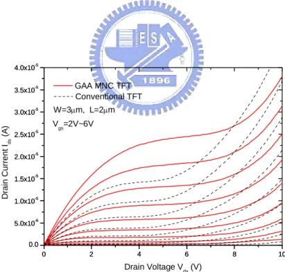
Fig. 2-9 Output characteristics of gate-all-around poly-Si TFTs with multiple nanowire channels and conventional TFTs. ...50
Fig. 2-10 The electron density simulation of gate-all-around poly-Si TFTs with multiple nanowire channels by ISE-DESSIS. ...51
Fig. 2-11 The parasitic S/D extension resistance of gate-all-around poly-Si TFTs with multiple nanowire channels. ...52
Fig. 2-12 The parasitic S/D extension resistance of conventional TFTs. ...52
Fig. 2-13 The corresponding SEM image of the extended bottom gate. ...53
Fig. 2-14 The simulated cross-sectional structures for GAA-MNC and conventional TFTs. ...53
Fig. 2-15 The electron density simulation of n-channel gate-all-around poly-Si TFTs with multiple nanowire channels and conventional TFTs by ISE-DESSIS. ...54
Fig. 2-16 Leakage current of gate-all-around poly-Si TFTs with multiple nanowire channels and conventional TFTs. ...54
Fig. 2-17 Leakage current mechanisms. ...55 (1) Thermionic emission
(2) Thermionic filed emission
(3) Pure tunneling (ban-to-band tunneling)
Fig. 2-18 The electric field simulation of gate-all-around poly-Si TFTs with multiple nanowire channels and conventional TFTs by ISE-DESSIS. ...56
Fig. 2-19 Gate current of gate-all-around poly-Si TFTs with multiple nanowire channels and conventional TFTs. ...56
Chapter 3
Fig. 3-1 Transfer characteristics of gate-all-around poly-Si TFTs with multiple nanowire channels before and after 1hr NH3 plasma passivation. ...57
Fig. 3-2 Output characteristics of gate-all-around poly-Si TFTs with multiple
nanowire channels before and after 1hr NH3 plasma passivation. ...57
Fig. 3-3 Transfer characteristics of conventional TFTs before and after 1hr NH3 plasma passivation. ...58 Fig. 3-4 Output characteristics of conventional TFTs before and after 1hr NH3 plasma passivation. ...58 Fig. 3-5 Normalized transfer characteristic of gate-all-around and bevel-side-gate poly-Si TFTs with multiple nanowire channels. ...59 Fig. 3-6 Output characteristics of gate-all-around and bevel-side-gate poly-Si TFTs with multiple nanowire channels. ...59 Fig. 3-7 Normalized transfer characteristics of bevel-side-gate poly-Si TFTs with multiple nanowire channels and conventional TFTs. ...60 Fig. 3-8 Output characteristics of bevel-side-gate poly-Si TFTs with multiple
nanowire channels and conventional TFTs. ...60
nanowire channels and conventional TFTs. ...61 Fig. 3-10 Output characteristics of gate-all-around poly-Si TFTs with multiple nanowire channels and conventional TFTs. ...61 Fig. 3-11 Transfer characteristics of gate-all-around poly-Si TFTs with multiple nanowire channels and conventional TFTs. ...62
Fig. 3-12 Output characteristics of gate-all-around poly-Si TFTs with multiple nanowire channels and conventional TFTs. ...62 Fig. 3-13 Normalized transfer characteristics of gate-all-around poly-Si TFTs with multiple nanowire channels. ...63 Fig. 3-14 Normalized transfer characteristics of conventional TFTs. ...63 Fig. 3-15 The threshold voltage of poly-Si TFTs with multiple nanowire channels and conventional TFTs with various channel length. ...64 Fig. 3-16 Normalized transfer characteristics of gate-all-around poly-Si TFTs with multiple nanowire channels. ...65 Fig. 3-17 Normalized transfer characteristics of gate-all-around poly-Si TFTs with multiple nanowire channels. ...65 Fig. 3-18 Normalized transfer characteristics of conventional TFTs. ...66 Fig. 3-19 Normalized transfer characteristics of conventional TFTs. ...66 Fig. 3-20 The threshold voltage of poly-Si TFTs with multiple nanowire channels and conventional TFTs with various channel width. ...67 Fig. 3-21 Normalized transfer characteristics of the GAA-MNC TFTs with various stress times. ...68 Fig. 3-22 Normalized transfer characteristics of the conventional TFTs with various stress times. ...68
Fig. 3-23 Threshold voltage shift of the GAA-MNC and conventional TFTs with
various stress times. ...69
Fig. 3-24 The cross-section schematic image of the silicon nanotips. ...70
Fig. 3-25 The layout of silicon nanotips. ...70
Fig. 3-26 The related optical microscope image of silicon nanotips. ...71
Fig. 3-27 The related optical microscope image of silicon nanotips. ...71
Fig. 3-28 The top view SEM images of Si nanotips. ...72
Fig. 3-29 The tilted view SEM images of Si nanotips. ...72
Fig. 3-30 The cross-section view SEM images of Si nanotips. ...73
Fig 3-31 The schematic of a source measure unit (Keithley 237). ...73
Fig. 3-32 The field emission I-V plot. ...74
Fig. 3-33 The field emission I-V plot. ...74
Chapter 1
Introduction
Recently, low temperature polycrystalline silicon (LTPS) thin film transistors (TFTs) have received much attention because of their increasing use in active matrix displays, such as active matrix liquid crystal displays (AMLCDs) [1.1] and active matrix organic light emitting displays (AMOLCDs) [1.2], and potential for the application on three-dimension integrated circuits (3-D ICs) [1.3]. The LTPS TFTs exhibit superior performance than a-Si TFTs, such as higher mobility and better reliability. Therefore, there is great interest in improving the performance of LTPS TFTs. In this chapter, an overview of LTPS TFTs is provided and the key fabrication processes and the electrical characterization of LTPS TFTs are reviewed.
1-1 An Overview of Low Temperature Poly-Si (LTPS)
TFTs
The study of polycrystalline silicon (poly-Si) thin film transistors (TFTs) fabricated using a maximum temperature below 600 ℃ commenced in 1980s. The original motivation of this concept was to replace quartz with low-cost glass for active matrix display applications. This would make large-area high-definition active matrix displays more practical and less expensive.
Previously, poly-Si TFT technology was primarily applied on small, high-definition LCD panels for projection display systems, because the high processing temperature typically required made it incompatible with commercially available large-area glass substrates and necessitated the use of quartz substrates. In recent years, however, rapid progress has been made in the development of fabrication processes which are compatible with glass substrates and also in the improvement of process-module throughput, so that the cost-effective manufacture of LTPS TFT AMLCDs and AMOLCDs on large-area substrates now appears.
Modification of process procedure for reducing fabrication cost and enhancing TFT performance is another issue in the fabrication of LTPS TFTs on large-area glass substrates. Self-aligned processes are very attractive for advanced circuit systems on large-area glass substrates, while reducing masks and process steps can effectively promote production yield and reduce fabrication cost.
In the following sections, more detailed information about fabrication processes such as crystallization and defect passivation are introduced to give an overall concept of LTPS TFT technology.
1-2
Crystallization of Amorphous Silicon (A-Si)
Thin Films
Crystallization of a-Si thin films has been considered as the most important process in the fabrication of LTPS TFTs. The crystallized poly-Si thin films always serve as active layer/or channel in the poly-Si TFTs. As a result, the quality of crystallized poly-Si thin films profoundly affects the performance of poly-Si TFTs. The defect density is generally a gauge for assessing the quality of poly-Si. Reducing defect density in polycrystalline material will make it approach the quality of single-crystalline material, which will lead to better performance of polycrystalline device. In polycrystalline material, most of defects are always generated in the grain boundaries. Essentially, enlarging grain size can reduce the quantity of grain boundaries. Hence, enlarging grain size can effectively promote the quality of poly-Si. As-deposited poly-Si generally exhibits small grain size, which results in inferior characteristics of poly-Si device. On the other hand, poly-Si re-crystallized from a-Si usually possesses larger grain size compared to the as-deposited one. This is why the re-crystallized poly-Si is always used in most poly-Si device applications.
In the last two decades, various technologies have been proposed for a-Si crystallization on foreign material. They are always classified into two groups: solid phase crystallization and liquid phase crystallization. In solid phase crystallization, thermal annealing provides the energy required for grain nucleation and growth. In general, intrinsic solid phase crystallization needs a long duration to fully crystallize a-Si at low temperature, and large defect density always exists in crystallized poly-Si. In liquid phase crystallization, a laser is usually employed to melting the silicon thin
film. In some cases, liquid phase crystallization is always referred to laser crystallization.
In the following, three kinds of low temperature crystallization methods, which have been most widely studied, are roughly reviewed, including solid phase crystallization (SPC), laser crystallization (LC), and metal-induced crystallization (MIC).
1-2-1 Solid Phase Crystallization
Thin films deposited in the amorphous state and then crystallized into poly-Si have been shown to have higher carrier mobility [1.4] due to the large grain size compared to thin films deposited in the polycrystalline state. For thin films deposited at temperatures below 600 °C, thermal crystallization for several hours (~ 20 hour) at 600 °C is required to convert them into final polycrystalline form. The grains resulting from this process are generally elliptical in shape due to preferential growth in the <112> direction [1.5], and dendritic due to the formation of twin along (111) boundaries. However, due to the low temperature used, long crystallization durations of several hours are necessary, and large defect density exists in crystallized poly-Si.
An alternative to enlarge grain size of poly-Si is to modify the structural disorder of the starting a-Si. Previous studies indicated that a significant enlargement of grain size of crystallized poly-Si could be achieved by increasing the initial structure disorder of the silicon network [1.6]. The high structure disorder of the Si network increases the active energy required to nucleate Si, thus, reduces the nucleation rate during the thermal annealing. Therefore, the grain size is enlarged due to the reduction of nucleation seeds. The disorder of the silicon network can in turn be increased by utilizing low deposition temperatures combined with high deposition rates. Disilane (Si2H6) has been shown to have higher deposition rates and lower deposition temperatures than siliane (SiH4) using pyrolytic chemical vapor deposition (CVD). Hence, crystallization of a-Si thin films deposited by thermal decomposition of disilane yield very large grain size [1.7].
1-2-2 Metal Induced Crystallization
It is well known that SPC temperatures of a-Si can be lowered by the addition of certain metals. When a certain metal, for example, Al, Cu, Au, Ag, Pd, or Ni, is deposited on a-Si, the a-Si crystallizes to poly-Si at a lower temperature than its SPC temperature. Generally, such behavior is called as “metal induced crystallization (MIC)”. The reaction between a metal and a-Si occurs at an interlayer by diffusion and it lowers the crystallization temperature [1.8]. Such enhancement of crystallization is due to an interaction of the free electrons from the metal with covalent Si bonds near the growing interface. Considering the metal-Si eutectic temperature, an a-Si thin film can be crystallized at below 500°C. However, in spite of low crystallization temperature, metal contamination is a serious problem in metal-induced crystallized poly-Si.
Palladium (Pd) or nickel (Ni) was found to induce crystallization of a-Si outside its coverage area [1.9]. This phenomenon of metal induced “lateral” crystallization, or MILC for short, has been found to produce polycrystalline silicon thin films largely free of metal contamination, with better crystallinity than those produced by SPC. Among various metals, Ni has been shown to be the best candidate of inducing lateral crystallization at low temperature for fabricating good-performance poly-Si TFTs. A large amount of reports have demonstrated that good-performance LTPS TFTs can be fabricated using Ni metal induced lateral crystallization (Ni-MILC) [1.8]-[1.10].
1-2-3 Laser Crystallization
A presently widely used method to prepare poly-Si on foreign substrates is laser crystallization. Laser crystallization is a much faster process than SPC and MIC and can produce large grained poly-Si with a low dislocation density. The basic principle of laser crystallization is the transformation from amorphous to crystalline silicon by melting the silicon for a very short time without damaging the glass substrate [1.11]-[1.12]. The laser modes can mainly be divided into two types, pulse type and continuous wave laser type. The excimer laser emits in UV light region with short pulse duration (10-30ns) by the laser source of ArF, KrF, or XeCl (output wavelengths 193, 248, and 308nm, respectively) gas. On the other hand, the continuous wave (CW)
laser emits in green light by the diode-pumped solid-state (DPSS) laser source of Nd:YVO4 (532nm) [1.13].
The benefit of using excimer laser crystallization (ELC) is the strong optical absorption of a-Si thin film to UV lights. During ELC process, a-Si thin films absorb the light, then melt and recrystallize in a short period of time, forming poly-Si grain (~1μm). For the volume expansion from liquid to solid phase, surface roughness (usually called protrusion) occurs after the ELC process. It has been reported that increasing the laser shots will reduce the protrusion and obtain better crystallinity. The definition of laser shots is the overlaps between each laser shot, i.e., 20 shots correspond to 5% overlap per shot. The poly-Si thin film fabricated by ELC suffers from narrow process window and instability of shot-to-shot laser energy, which lead to non-uniformity issue of grain structure.
Unlike ELC, poly-Si thin film fabricated by CW laser exhibits less protrusion and better uniformity. The power instability is less than 1%, which is superior to that of excimer laser. The continuous wave characteristic makes it possible for grain to grow in a large longitudinal distance (tens of μm in average). However, the technology has not been well-development and is still under investigation in modern academic research.
1-3
Defect Passivation
The electrical behavior of a poly-Si TFT is dominated by the effects of defect states within the poly-Si thin film. The high density of defect states result in poor device performance, such as low field-effect mobility, large leakage current, large threshold voltage, and large subthreshold swing. The incorporation of hydrogen into the channel layer (also called hydrogenation) to passivate the defect states is effective and essential for attaining good device performance and also for improving the uniformity of device performance. Because significant hydrogen diffusion occurs at temperatures above 350°C, the defect passivation process must be performed after all the high-temperature-processing steps in the poly-Si TFT fabrication process, consequently, the channel poly-Si thin film may be covered by one or more layers which can significantly impede the defect passivation process.
There are four methods that have been used to date to introduce hydrogen into channel poly-Si thin film including furnace annealing, radio-frequency (RF) plasma, solid-source diffusion, and H+ ion implantation. Simple annealing in H2 ambient is not sufficient for poly-Si TFTs due to poor diffusivity of molecular hydrogen in silicon. RF plasma exposure in a parallel-plate reactor is widely used as it has resulted in excellent TFT performance. However, very long process times are usually required for the passivating species to diffuse into the channel poly-Si thin film, so that the throughput of this method is unacceptably low. However, with the use of a low-temperature (< 300 °C) source/drain formation process (e.g. employing ion-shower doping), it is possible to perform the hydrogenation step prior to the deposition of gate dielectric and gate electrode layers, so that the throughput issue for this step can be eliminated.
On the other hand, it has been reported that TFTs exposed to hydrogen plasma suffer from poor hot carrier endurance and a low thermal stability due to the weak Si-H bond [1.14]. NH3 and N2 have also been proposed instead of H2. Better hot carrier endurance has been shown as the Si-N bond is stronger than Si-H bond [1.14]. Alternative approach, which generates high-density plasma, such as electron cyclotron resonance (ECR) and transformer coupled plasma (TCP), may result in equivalent performance with high throughput [1.15].
Solid-source diffusion refers to the process of depositing a SiNx passivation layer with extremely high concentrations of hydrogen. Rather than requiring a separate hydrogen or nitrogen plasma deposition step to repair the dangling bonds, a high hydrogen concentration passivation layer is deposited by PECVD followed by a short thermal anneal at 450 °C. This process may result in good TFT performance and uniformity while improving factory throughput and minimizing additional tool costs. It is perhaps the lowest cost hydrogenation approach.
The hydrogen can also be introduced into channel poly-Si thin film via ion implantation. The high-energy hydrogen implantation is substituted for H2 plasma step. However, expensive equipment and relative high doses (> 1016 cm-2) are required. In addition, it requires an additional annealing step at 250 ~ 400 °C as long as 1 hour to anneal out the damage.
1-4 Device Structures of LTPS TFTs
The advantage of LTPS TFTs is that they can be fabricated on various substrates. It allows us to replace Si wafer with large area and low cost glass or plastic substrates. The conventional TFTs can be divided into bottom-gate and top-gate structures. The bottom-gate structure offers some advantages for AMLCD applications. For example, good interface control can be achieved due to the ability to deposit the gate dielectric and precursor silicon sequentially in a single system without exposing to atmosphere ambient.
The top-gate structure is the most commonly used for poly-Si TFTs in AMLCD applications. Its self-aligned source/drain regions provide low parasitic capacitances, which are advantageous for achieving good display performance. Because the top-gate TFTs can achieve self-alignment more easily, this architecture is very suitable for device scaling down.
Recently, any new structures have been proposed to enhance TFT performance, such as the field-induced drain [1.16], the active poly-Si gate [1.17], the multi-gate structure [1.18], the elevated channel structure [1.19], the gate-overlapped LDD structure [1.20], and the four-terminal TFT structure [1.21] etcetera. Most of the newly developed structures can effectively improve the characteristics of conventional TFTs, especially in decreasing the anomalous leakage current in the off-state of poly-Si TFTs. In general, the reliability of poly-Si TFTs can also be enhanced by utilizing these structures because of the reduction of electric field near the drain junction.
1-5 Motivation
The CMOS (complementary metal oxide semiconductor) technology is pushed with continuous scaling-down for tremendously large density and functionalities. Similarly, the technology of poly-Si TFTs is approaching in the same trend. For SOP and 3-D ICs applications, it is necessary to fabricate high performance and small-dimension poly-Si TFTs for high density and low power circuits. There are some prior arts focusing their research on this way. In prior works of poly-Si TFTs, Y.
C. Wu et al. proposed poly-Si TFTs with multiple nanowire channels [1.22]. The experiment results demonstrate that the electrical performance increase with increasing the number of channels. Additionally, the high performance also contributes to the structures varied from single-gate to tri-gate operation. The same width TFTs with more channels exhibits superior and uniform characteristics, including a low leakage current, a high ON/OFF drain current ratio, a steep subthreshold slope, an absence of DIBL. However, it requires expensively advanced e-beam lithography which drastically increases cost and lower throughputs. C. J. Su et
al. present poly-Si nanowire TFTs with three gate electrodes, and its fabrication is
free of any advanced lithography [1.23]. With the three-gate operations, excellent electrical characteristics such as high ON/OFF current ratio and sharp subthreshold slope are obtained. The strong gate-coupling effect of these multiple gates, together with the tiny body of NW channels results in the observed improvement. However, the process sequence and gate operations of the three gate electrodes are very complicated with three individual gates.
In order to fabricate high performance poly-Si TFTs to meet requirement of SOP and 3-D ICs, we introduce a novel LTPS TFTs structure with simple and low-cost process. There are two aspects in our work. One is gate-all-around structure, and the other is multiple nanowire channels. Both aspects are briefly described below.
1-5-1 Gate-All-Around Structure
It is well-known that single-crystalline-Si MOSFETs are scaled down continually to meet the Moore’s Rule to achieve higher circuit density and operation speed. With the same trend, scaled-down poly-Si TFTs are also required to have higher integrated density in SRAMs and DRAMs and to increase driving current (i.e. operation speed) in peripheral circuits of AMLCDs and AMOLCDs. However, there are several short-channel effects in the conventional scaled-down poly-Si TFTs, such as threshold voltage roll-off, higher drain-induced barrier lowering, and kink effect. Additionally, the grain boundary defects and floating body structure in channel region in poly-Si TFTs cause more serious short-channel effects than other devices.
It has been demonstrated that the device performance can be enhanced with multi-gate structures. These structures, including double-gated, triple-gated, Π-gated,
Ω-gated, NW channel, and gate-all-around (GAA) [1.24]-[1.35], are concentrated on increasing the channel controllability. By using those structures, better gate control ability and higher driving current can be obtained. The short-channel effect can be alleviated with the strong gate controllability if the channel region is fully depleted [1.36]. The increased gates provide better electrostatic control in the channel, and therefore reduce the short-channel effects. The GAA structure has been considered to have the best gate controllability among those mentioned above, because the number of gates in GAA structure is maximum.
1-5-2 Multiple Nanowire Channels
The grain boundary defects presented in the poly-Si channel drastically degrade the performance of poly-Si TFTs. There are some aspects to improve the grain boundary effects in the channel, such as passivating the dangling bonds at grain boundary and reducing the number of grain boundary. In the view of reducing grain boundary, the poly-Si TFTs with multiple nanowire channels has been reported to effectively decrease the grain boundary defects in poly-Si channels [1.37]. Additionally, the NH3 plasma passivation has been reported more efficiently to passivate the grain boundary defects in multiple nanowire channels structures [1.38].
The nanowire structures have been receiving growing attention because the nanowire structures demonstrate some unique characteristics because high surface area, large surface-to-volume ratio and small size. The short-channel effects in nanoscale devices with nanowire channels is suppressing because the channel potential is better controlled in nanowire structures [1.39]. As a result, the nanowire channels exhibit superior electrical characteristics.
1-6 Thesis Outline
In chapter 1, a brief overview of LTPS TFTs technology is given to explain the device structures and defect passivation. The motivations of this work are subsequently explained to introduce this thesis.
thin-film transistors with multiple nanowire channels (GAA-MNC TFTs) are introduced. The important processes are analyzed by scanning electron microscope (SEM) and transmission electron microscope (TEM). And, the electrical characteristics of GAA-MNC TFTs are investigated.
In chapter 3, more unique electrical characteristics, such as NH3 plasma passivation, geometry, short-channel effects and narrow width effect in GAA-MNC TFTs are also introduced to discuss their mechanisms.
Chapter 2
Fabrication Sequence and Material
Analyses for Gate-All-Around Poly-Si TFTs
with Multiple Nanowire Channels
2-1 Introduction
Currently, low-temperature polycrystalline silicon (LTPS) technology is the most promising method to fabricate high performance thin-film transistors (TFTs) on glass or plastic substrate [2.1]. In comparison with amorphous silicon (a-Si) TFTs, LTPS TFTs exhibit higher field effect-mobility and better reliability, which lead to higher driving current and better stress resistance. As a result, LTPS TFTs are attractive for their application to liquid crystal display, such as pixel switches, drivers, and peripheral control circuit in active matrix liquid crystal displays (AMLCDs) [2.2] or active matrix organic liquid crystal displays (AMOLCDs) [2.3]. In recent years, poly-Si TFTs have been broaden their application to memories [2.4]-[2.5].
For these applications, scaled-down LTPS TFTs with high performance are required. The scaled-down devices enable higher circuit density in SRAMs and EEPROMs, and increase the driving current and speed of peripheral driving circuit in AMLCD application. Unfortunately, several short-channel effects are known to aggravate with reducing device dimension, such as threshold voltage roll-off, higher subthreshold swing, larger drain-induced barrier lowering (DIBL), and acuter kink effect. The short-channel effects seriously restrict these applications. Recently, for single-crystalline Si-on-insulator (SOI) Metal-Oxide-Semiconductor Field Effect Transistors (MOSFETs), lots of efforts on non-planar device structures have been developed for better gate electrostatic control of the channel potential, such as double-gated, triple-gated, Π-gated, Ω-gated, NW fin-channel, and gate-all-around (GAA) [2.6]-[2.17]. Among those structures, the GAA structure with nanowire channels is proposed to be the best structure to provide the immunity of short-channel effects. Additionally, the poly-Si TFTs suffer more serious short-channel effects than
SOI devices due to the presence of grain boundary and intra-grain defects in channel region. However, there are few works presented such structures on poly-Si TFTs so far. Besides, those works are required complicated processes or advanced lithography technology, which increase the process cost and decrease the fabrication yield. In this work, the gate-all-around poly-Si TFTs with multiple nanowire channels, for the first time, are proposed with using simple process to achieve high electrical performance and effectively suppress the short-channels effects.
2-2
Fabrication Sequence of Gate-All-Around
Poly-Si TFTs with Multiple Nanowire Channels
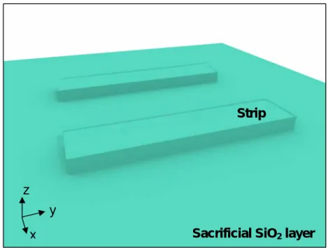
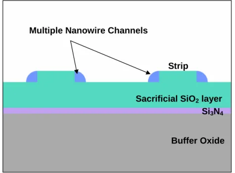
The fabrication steps of the GAA-MNC poly-Si TFTs are schematically illustrated in Fig. 2-1. At First, a 50 nm Si3N4 and a 300 nm SiO2 served as the etch-stop layer and the sacrificial layer were deposited on the oxidized wafer by the low-pressure chemical vapor deposition furnace (LPCVD) at 580 ℃ and 700 ℃, respectively. The sacrificial SiO2 layer was patterned as several strips by standard optical lithography and then etched anisotropically with 100 nm in-depth by the reactive ion etching (RIE) to form the steps as shown in Figs. 2-1(a) and (b) in the tilted and cross-section views, accordingly. Next, a 100 nm a-Si layer was conformally deposited on sacrificed layer for active layer by LPCVD at 550 ℃. After that, the active region was patterned only on the source, drain and the end of strips by transformer-coupled plasma reactive ion etching (TCP-RIE) as shown in Figs. 2-1(c) and 2-1(d) in the tilted and cross-section views, respectively. HBr and O2 are used as etching gas sources in TCP-RIE. The recipe is selected here because it has higher selectivity to SiO2 sacrificial strips (50:1) and can precisely control the dimension with slower etching rate (2 nm/sec). Due to the step profile of strips, the spacer nanowires were remained along the sidewalls of the strips after etching. It should be noted that the nano-scale dimension of the nanowire channels can be defined only by controlling the RIE time without any advanced lithography [2.18], each dummy strip produces twin nanowire channels, as well as the multiple channels can be designed with patterning several dummy strips (n strips x 2 wires/strip = 2n wires). Then, the solid phase crystallization (SPC) was performed at 600 for 24 hours to transform ℃
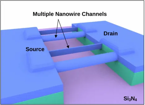
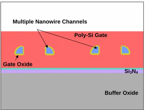
the a-Si into poly-Si. After that, the suspending channels were formed by etching the sacrificial SiO2 layer with 3:50 diluted HF, and the etching-stopper layer would stop etching process down to the buried oxide as shown in Figs. 2-1(e) and 2-1(f) in the tilted and cross-section views, respectively. Then a 25 nm SiO2 and a 200 nm phosphorous in-situ doped poly-Si were deposited conformally around the suspending channels as the gate insulator and gate electrode, respectively. The gate was defined as shown in Figs. 2-1(g) and 2-1(h) in the tilted and cross-section views, respectively, and a phosphorous ion implantation was performed with a dosage of 5×1015 cm-2 and a energy of 30 keV followed by source/drain activation at 600 for 10 hours and 300 ℃ nm SiO2 passivation layer, sequentially. The contact holes were patterned to etch the passivation layer by two steps of RIE and HF (1:50) immersion. Then, the Ti/TiN/Al-Si-Cu/Ti metal layers were deposited by sputter systems, and the metal pad were patterned and etched by RIE. Finally, NH3-plasma passivation was carried out for 1 hour [2.19]. For the purpose of comparison, the conventional poly-Si TFTs with single top-gated structure were also fabricated at the same process run.
2-3 Material Analyses for Gate-All-Around Poly-Si
TFTs with Multiple Nanowire Channels
The previous section briefly describes the process sequence of the GAA-MNC TFTs. In this section, the scanning electron microscope (SEM) and transmission electron microscope (TEM) have been used to analyze the detailed process parameter in the fabrication of GAA-MNC TFTs.
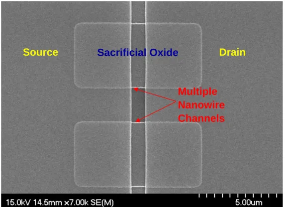
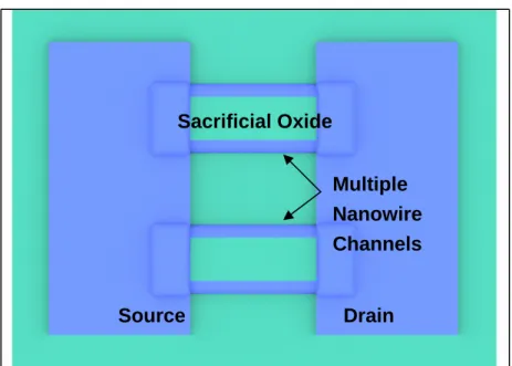
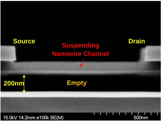
Figures 2-2(c) and 2-2(d) display the schematic images before and after sacrificial oxide stripping by HF acid, respectively. And, Figs. 2-2(a) and 2-2(b) show their corresponding SEM image. It can be shown that the sacrificial SiO2 layer has been removed and there are two suspending nanowires remained after oxide stripping. Figure 2-3(a) demonstrates the tiled-view SEM image of the multiple nanowire channels after HF etching. The corresponding process step is demonstrated in Fig. 2-3(b). Different channel width can be easily designed by adjusting the number of sacrificial SiO2 strips. The structure of suspending channels is displayed in the cross-section view in the SEM image of Fig. 2-4(a). The corresponding process step is demonstrated in Fig. 2-4(b) The multiple nanowire channels are hung in the air with a
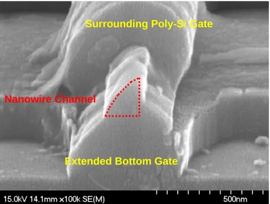
height 200 nm above the Si3N4 etch-stop layer and joined to the source and drain pads. With the aid of the suspending nanowire channels, the gate insulator and gate electrode deposited by LPCVD can be easily surrounding the channel to form the GAA structure. Figure 2-5(a) shows the top view SEM graph after patterning gate. The corresponding process step is demonstrated in Fig. 2-5(b). The multiple channels are surrounded by in-situ doped poly gate. It should be noted that there are additional bottom gates remained below the source/drain extension after gate patterning. The source/drain extension shields the additional bottom gates from the anisotropic reactive ion etching. The cross-section SEM graph can specifically demonstrate the residual bottom gate below the nanowire in Fig. 2-6(a). The corresponding process step is demonstrated in Fig. 2-6(b)
Figure 2-7 exhibits the cross-section transmission electron microscope graph of each gate-all-around nanowire. The polycrystalline nanowire channel in the center of graph is formed by the TCP-RIE and the dimension of nanowire is precisely controlled by duration of etching. The TEM graph shows that the vertical sidewall thickness, the horizontal width and bevel length of each NW channel are about 85 nm, 85 nm, 130 nm, respectively. Thus the total surrounding width of each NW channel is 300 nm. Moreover, the good step coverage of poly gate and gate oxide film is observed on the GAA structure. That is, the 25 nm TEOS gate oxide and 200 nm phosphorous in-situ doped poly gate are conformally deposited around the nanowire channel. It also demonstrates that the grain size in the nanowire channel after the solid phase crystallization at 600 for 24 hours℃ is less than 100 nm.
2-4 Electrical Characterization of Gate-All-Around
Poly-Si TFTs with Multiple Nanowire Channels
In this section, the electrical characteristics of GAA-MNC TFTs were measured by the HP 4156c semiconductor parameter analyzer.
The constant drain current method is used to determinate the threshold voltage. The threshold voltage (Vth) is defined as the gate voltage required to achieve a normalized drain current as 10nA at Vds = 0.1 V
10nA….………..(2-1)
L W V
Vth = gs @Ids = ×
where the W and L are the channel width and length, respectively. It should be noted that the channel width of GAA-MNC TFT is defined as 0.6n μm, where the n is the designed number of dummy strip. That is, W = n strips × 2 wires/strip × 300 nm/wire = 0.6n μm. The surrounding width of each nanowire channel is 300 nm as shown in Fig.2-7. The subthreshold swing (SS) is determined from the subthreshold region of Ids-Vgs curve at Vds = 0.1 V. V V .…………..(2-2) V I ds gs ds) @ 0.1 min SS ⎟⎟ = ∂ = log( 1 ⎠ ⎞ ⎜ ⎜ ⎝ ⎛ ∂ −
The mobility is calculated at Vds = 0.1 V by
.………....(2-3) ds ox m V g L C W × × × = μ
where the gm is the maximum transconductance defined by
………..(2-4) gs ds m V I g ∂ ∂ =
and the Cox is the gate capacitance per unit area. The ION/IOFF current ratio is defined as the ratio of maximum/minimum value of Ids-Vgs curve at Vds = 2 V. The drain-induced barrier lowering (DIBL) is defined as V△ gs/ V△ ds at Ids = 10-8 A.
The electrical characteristics from the GAA-MNC and conventional TFTs with different geometry dimension will be further discussed in the chapter 3. In this section, the major parameters are extracted from devices with channel length of 2 μm and channel width of 3 μm. The 3-μm channel widths of GAA-MNC TFTs are defined by 5-dummy-strip structure (i.e. 5 strips × 2 wires/strip × 300 nm/wire = 3 μm).
Figure 2-8 demonstrates the comparison of transfer characteristics between GAA-MNC and conventional TFTs, while the comparison of output characteristics is demonstrated in Fig. 2-9. Those figures display that the GAA-MNC TFTs exhibit excellent electrical performance as compared to conventional TFTs. The mobility increases from 26 to 33 cm2/V-s, the threshold voltage V decreases from 2.31 to 1.31
V, the subthreshold swing SS decreases from 0.64 to 0.37 V/decade, minimum IOFF decreases from 3.69×10⁻¹² to 3.33×10⁻¹³ A, maximum ION increases from 3.81×10⁻⁵ to 4.17×10⁻⁵ A, ION/IOFF increases from 1.03×10⁷ to 1.25×10⁸, and DIBL decreases from 0.29 to 0.04 V/V.
In the subthreshold and on-state region, the GAA-MNC TFTs demonstrate lower threshold voltage Vth , lower DIBL, stepper subthreshold swing SS , higher on current and higher mobility. The mechanisms of the performance improvement are explained as follow.
I. Surrounding-Gate Effect
The better gate controllability of gate-all-around transistors has been reported [2.14]. The result is also obtained in this work. With the additional gates, the channel potential can be effectively controlled. Because the channel is well-controlled, the GAA-MNC TFTs can turn on easily and result in shaper subthreshold swing, lower threshold voltage and smaller DIBL. Also, the higher gate electric field can suppress the lateral electric field in drain and reduce the influence caused from drain bias such as DIBL and kink effects. The high electric field induces local volume inversion, many studies indicate that the carriers in the volume region of channel have higher mobility than those in the surface due to the mobility in surface is reduced by surface scattering [2.20]-[2.21].
II. Sharp Corner Effect
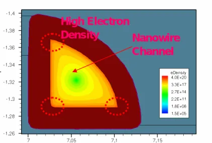
The three sharp corners in each nanowire enhance the gate electric field due to the geometry and then provide more carriers during on state. This phenomenon is further explained by a simulated analysis of ISE-DESSIS. Figure 2-10 shows the cross-section simulation of GAA-MNC TFTs. It shows that the three sharp corners inverse more electrons than other region, the electron density increase from 1018 to 1020 cm-2.
III. Nano Dimension
Fewer intra- and inter- grain defects exist in the nanowire channels owing to the high surface-to-volume ratio and small volume of nanowire body in the GAA-MNC TFTs. The higher surface-to-volume ratio indicates that the GAA-MNC TFTs have less volume defects than conventional TFTs in the same surface width.
The parasitic resistance can be extracted from the output characteristics of transistors with various channel length at low drain voltage and high gate voltage. The ON resistance can be expressed as
p ch ds ds on R R I V R = + ∂ ∂ = ………..(2-5)
where the Rch and Rp represent the channel resistance and parasitic resistance. The parasitic resistance can be extracted by plotting Ron versus channel length with different gate bias. Then, the Rp is obtained in the merged point of all linear fitting lines. It has been reported that the FinFETs suffer from higher source/drain extension resistance than the conventional devices [2.22]-[2.23]. However, in this study, the parasitic S/D resistance of the GAA-MNC TFT (12.17 kΩ) is comparable to that of conventional TFT (12.09 kΩ) as shown in Figs. 2-11 and 2-12. It is explained by the additional contribution of the parasitic extended bottom gate of the GAA which exists below the extended nanowire S/D. Figure 2-13 shows its corresponding SEM image. For further explanation, a simulated analysis was performed by ISE-DESSIS. Figure 2-14 shows the simulated cross-sectional structures for GAA-MNC and conventional TFTs, and Fig. 2-15 displays their electron density and doping concentration at Vgs = 15 V and Vds = 0.1 V. During the on-state operation, the extended bottom gate can serve as an additional field plate to increase the electron density from 5×10¹⁹ to 7.19×1019 cm-3 in the extended nanowire S/D, which effectively lowers the parasitic S/D resistance.
The leakage currents of GAA-MNC and conventional TFTs are specifically shown in Fig. 2-16. In the off-state region, the mechanisms of leakage current can be explained under three different gate-bias regions. The leakage current mechanisms are displayed in Fig. 2-17. In low electric field region, the electrons are thermally excited from the valence band into the trap states and then jumping into the conduction band. The phenomenon is called thermionic emission which contributes the low electric field off-state leakage current. The number of excited electrons in thermionic emission strongly depends on the quantity of the defects and traps in channel.
In medium electric field region, the electrons are thermally excited from the valence band into the trap states and then tunneling into the conduction band by the gate-drain electric field. This mechanism is known as thermionic-filed emission and
depends on both the trap states and electric field.
In high electric field region, the band diagram is bent strongly under high gate-drain electric field in the gate/drain overlapped region. The electrons tunnel directly from the valence band to the conduction band. This is called as the band-to-band tunneling and cause high leakage current in gate-drain junction which is also known as gate-induced drain leakage (GIDL). The GIDL current highly depends on the gate-to-drain electric field and becomes more serious with the assistance of traps.
The GAA-MNC TFTs shows lower leakage current at the low gate electric field region as compared to conventional TFTs. It is because there is less volume defects in GAA-MNC TFTs’ channel resulting in the reduction of thermionic emission. However, at the high gate electric field region, the GIDL current is more significant in the GAA-MNC TFTs. The higher GIDL current comes from the higher gate electric field as a result of stronger gate controllability. Also, the three sharp corners enhance the electric field resulting in the high GIDL current. The related simulation results are shown in Fig. 2-19, the electric field in the three sharp corners is much higher than other regions. The higher gate leakage current also been observed in GAA-MNC TFTs because higher electric field in the three sharp corners as shown in Fig. 2-20. Even then, the lightly doped drain (LDD) and T-shaped gate structures have been used widely for reducing the electric field in drain junction and those structures are also suitable to apply on the GAA-MNC TFTs.
2-5 Summary
In this chapter, the gate-all-around poly-Si TFTs with multiple nanowire channels were successful fabricated with simple process. In the first part, the fabrication sequence of GAA-MNC TFTs is clearly introduced. There are two aspects used in fabricating the GAA-MNC TFTs. First, the a-Si spacers formed by anisotropic dry etch are used to fabricate multiple nanowire channels. The HBr and O2 are selected here as etching gas sources because it has higher selectivity to SiO2 sacrificial strips (50:1) and can precisely control the dimension with slower etching rate (2 nm/sec.). Second, The suspending nanowire after sacrificial oxide stripping is achieved to
establish the gate-all-around structure. In the second part, the material analyses for GAA-MNC TFTs are carried out by the scanning electron microscope and transmission electron microscope. Good conformal depositions of gate-oxide and poly-gate thin films were clearly observed. In the third part, the electrical characteristics of GAA-MNC TFTs are introduced and compared to conventional TFTs. The GAA-MNC TFTs exhibits excellent electrical characteristics as compared to conventional ones. Besides, the mobility increases from 26 to 33 cm2/V-s, the threshold voltage Vth decreases from 2.31 to 1.31 V, the subthreshold swing SS decreases from 0.64 to 0.37 V/decade, minimum IOFF decreases from 3.69×10⁻¹² to 3.33×10⁻¹³ A, maximum ION increases from 3.81×10⁻⁵ to 4.17×10⁻⁵ A, ION/IOFF increases from 1.03×10⁷ to 1.25×10⁸, and DIBL decreases from 0.29 to 0.04 V/V. Those improvements are contributed to the better gate controllability of GAA structures, three sharp corners, and less defects in nanowire channels. The parasitic S/D resistance of GAA-MNC TFTs is comparable to conventional TFTs. The leakage mechanisms are investigated. In low gate electric field region, the GAA-MNC TFTs show lower leakage current than conventional ones owing to less defects. In high electric field, the higher GIDL current is observed in GAA-MNC TFTs. The higher gate electric field in GAA-MNC TFTs results from the stronger gate controllability and three sharp corners.
Chapter 3
Investigation of Characteristics of
Gate-All-Around Poly-Si TFTs with
Multiple Nanowire Channels
3-1 Introduction
In chapter 2, the electrical characteristics of gate-all-around poly-Si TFTs with multiple nanowire channels (GAA-MNC TFTs) are investigated and discussed. In this chapter, further electrical characteristics are studied. The NH3 plasma passivation issue will be discussed at first. Second, in the view of geometry, the TFTs with different geometry are compared. The short-channels effects of GAA-MNC and conventional TFTs would take into consideration in the third part. Moreover, a unique narrow width effect is discussed in the third part. Finally, the application of nanowires with sharp corners on field emission devices is proposed.
3-2 NH
3Plasma Passivation
In comparison with single-crystalline silicon (c-Si), poly-Si is rich in grain boundary defects and intra-grain defects, and the electrical activity of these charge-trapping centers profoundly affects the electrical characteristics of poly-Si TFTs. The turn-on characteristics, such as threshold voltage, subthreshold swing, and mobility, of poly-Si TFTs are much inferior to those of c-Si devices due to the fullness of defect states in the device active region. Moreover, the density of defects in poly-Si film fabricated by low-temperature solid phase crystallization is very high. If there are more defects in channel, larger gate voltage is required to fill the greater number of traps to turn on. Carrier mobility is degraded by scattering with charge-trapping centers and surmounting the potential barrier height which is built by charged traps. It
has been reported the NH3 plasma treatment can improve the characteristics of poly-Si TFTs [3.1]. The hydrogen can passivate the dangling bonds in grain boundary and the nitrogen piles up at the SiO2/poly-Si interface.
Figure 3-1 exhibits the comparison of transfer characteristics between the GAA-MNC TFTs with and without 1 hour NH3 plasma treatment, while the comparison of output characteristics is exhibited in Fig. 3-2. For comparison, the characteristics of conventional TFTs also demonstrate in Figs. 3-3 and 3-4. The major parameters are listed in Table 3-1. After NH3 plasma treatment, the GAA-MNC and conventional TFTs reveal higher on current, higher mobility, steeper subthreshold swing and lower threshold voltage. The defects are passivated after NH3 plasma treatment, so the performances of GAA-MNC and conventional TFTs are improved. The GIDL currents of GAA-MNC and conventional TFTs decrease more than one order and the kink effect happens later at higher drain voltage. The kink effect and GIDL current are both related to the density of traps in active region and high electric field at the drain junction. The non-ideal increased current is suppressed when the dangling bonds are tied to the hydrogen and nitrogen. It is observed that the improvement of mobility in the GAA-MNC TFTs is higher than in conventional ones. That is because NH3 plasma passivation in multi-channel TFTs is more efficient than conventional single-channel TFTs as the exposed surface is increased [3.2].
3-3 Geometry Effects
In the previous chapter the superior performance of the GAA-MNC TFTs as compared to conventional top-gate TFTs was highlighted. Further, the bevel sidewall issue of the GAA-MNC TFTs will be discussed in this section.
The bevel sidewall is defined as the bevel edge of poly-Si spacer in the GAA-MNC TFTs’ channel. The curved surface of sidewall had been made by the conformal deposition of amorphous silicon and anisotropically reactive-ion etching, subsequently. The bevel-side-gate TFTs with multiple nanowire channels (BSG-MNC TFTs) were fabricated as same as the GAA-MNC TFTs without the sacrificial oxide stripping. It should be noted that the channel width of BSG-MNC TFTs is the summation of each nanowire channel width. The bevel sidewall width of each
nanowire channel is 130 nm as shown in Fig. 2-7. (5 strips × 2 wires/strip × 130 nm/wire = 1.3 μm).
Figure 3-5 displays the normalized transfer characteristics of the BSG-MNC and GAA-MNC TFTs, while the output characteristics are displayed in Fig. 3-6.
As compared to the GAA-MNC TFTs, the BSG-MNC TFTs indicated poor electrical characteristics. The GAA-MNC TFTs with surrounding gate and three sharp corners result in superior transfer characteristics as compared to the BSG-MNC TFTs. From the output characteristics, the BSG-MNC TFTs have 43% channel width of the GAA-MNC TFTs (i.e. 1.3 μm/3 μm × 100%) while only demonstrate 24.71% on-current of the GAA-MNC TFTs. This result is also further confirmed that the better gate controllability and three sharp corners in the GAA-MNC TFTs can provide more inversion carriers at on-state.
Figure 3-7 displays the comparison of transfer characteristics between the BSG-MNC TFTs and conventional TFTs, while the comparison of output characteristics is displayed in Fig. 3-8. The BSG-MNC TFTs show better subthreshold swing than conventional ones. This result is due to better gate controllability in non-planar surface of spacer sidewall and the nanowire channels. Compared to the conventional TFTs, the mobility of BSG-MNC TFTs is a little lower owing to the surface damage during spacer formation by the RIE etching.
In the study of TFTs with different geometry, the BSG-MNC TFTs with non-planar and nano-scale channels show better electrical characteristics than conventional planar TFTs. The GAA-MNC TFTs display better performance than BSG-MNC TFTs because the nanowire channels are surrounded by gate electrode.
3-4 Dimensional Scalability
Recently, poly-Si TFTs are attractive for their applications on active-matrix displays, such as pixel switches, drivers, and peripheral control circuit [3.3], [3.4]. Besides, poly-Si TFTs also have been broadened their applications on memories [3.5]-[3.6].
For these applications, scaled-down LTPS TFTs with high performance are much required. The scaled-down devices enable higher circuit density in SRAMs and EEPROMs, and increase the driving current and operation speed of peripheral driving
circuit in active-matrix applications. The short-channel and narrow-width effects of scaled-down devices are studied in this section.
3-4-1 Short Channel Effects
As the channel length shrank, there are several short-channel effects resulted in device characteristics. First, because the lateral electric field from drain bias becomes larger in short channel, the kink effect and drain-induced barrier lowering (DIBL) become more pronounced. Second, the threshold voltage becomes smaller and this phenomenon is well-known as threshold voltage roll-off. Moreover, the floating-body architecture and charge trapping by defect states result in serious avalanche induced effects in poly-Si TFTs [3.7]. The avalanche-induced effects become more severe as the TFT dimension is reduced due to the enhancement of impact ionization caused by the increasing electric field. Therefore, lot severe short-channel effects are shown in poly-Si TFTs as compared to the single-crystalline Si transistors.
Figure 3-9 demonstrates the comparison of the transfer characteristics between GAA-MNC and conventional TFTs, while the comparison of the output characteristics is demonstrated in Fig. 3-10. Those TFTs have channels length of 5 μm. The kink effect is not obvious. Figure 3-11 demonstrates the transfer characteristics of GAA-MNC and conventional TFTs, while the output characteristics are demonstrated in Fig. 3-12. Those TFTs have channels length of 2 μm. The DIBL in GAA-MNC TFT is 0.04 V/V, while that in the conventional TFT is 0.29 V/V. The kink effect is related the lateral electric field in channel and the amount of inversion carriers. As shown in output characteristics, the GAA-MNC TFTs exhibit suppressed kink effect even with higher current. The short-channel effects are suppressed due to the higher gate electric field which prevents the electric field penetration from the drain to the source.
Figures 3-13 and 3-14 show the normalized transfer characteristics of the GAA-MNC TFTs and conventional top gate TFTs, respectively. Those devices have the fixed channel width (W) of 3 μm and various channel length (L) from 1 μm to 5 μm. Obviously, the conventional TFTs show serious threshold voltage roll-off. The threshold voltage is extracted from normalized transfer characteristics and compared in Fig. 3-15 and Table 3-2. In conventional TFTs, the threshold voltage shifts from 2.88 V to 2 V as decreasing the channel length from 1 μm to 5 μm. There is negligible
threshold voltage roll-off in the GAA-MNC TFTs. The improvement of short-channel effects is attributed to the stronger gate controllability from the GAA structure with multiple nanowire channels.
3-4-2 Narrow Width Effect
As the channel width scaled down, the poly-Si TFTs are reported to show lower threshold voltage [3.8]. In this section, the shifts of threshold voltages between the GAA-MNC and conventional TFTs are compared.
Figures 3-16 to 3-19 show the normalized transfer characteristics of the GAA-MNC TFTs and conventional top-gate TFTs, respectively.
Those devices have the fixed channel length (L) of 2μm and 5μm with various channel width (W). It demonstrates that the threshold voltage decreases with the channel width decreasing in conventional TFTs. As compared to conventional TFTs, the threshold voltage of the GAA-MNC TFTs with various channel width is approaching constant. The threshold voltage is extracted from normalized transfer characteristics and compared in Fig. 3-20 and Table 3-3. The figure displays that the threshold voltage of conventional TFTs drops significantly as the channel width scaled down to 1μm or less, while there is negligible threshold voltage shift in the GAA-MNC TFTs. The reason is discussed below.
Due to the narrow-dimensional active island, the gate electrode is deposited not only on the surface channel width defined by the designed layout but also the two-side edges of this island. The two-side edges provide additional channel width which is two times of the thickness of the active layer. The edge channels show negligible influence as the channel width is large enough. But, as decreasing the channel width, the edge channels become comparable to the main (surface) channel. In narrow width devices, the edge channels provide additional current and lower the threshold voltage.
3-5 Reliability
The reliability of poly-Si TFTs is a major concern when they are applied to circuitry application such as SOP and 3-D ICs. In comparison with single-crystalline silicon, poly-Si is full of weak Si-Si bonds and Si-H bonds. These weak bonds are easily broken during device operation which results in the variation of device characteristics and circuit failure. When the devices are operated at large drain voltage, the conduction carriers can obtain energy from the high drain electric field and become “hot”. The hot carriers can cause avalanche impact ionization near drain junction and create lots of defect states. Serious performance degradation would be arisen in this drain avalanche hot carrier operation. In this section, the reliability comparison between the GAA-MNC and conventional TFTs under drain avalanche hot carrier stress is investigated. The stress condition is measured at Vds = 10 V and Vgs = Vth + 2.7 V. The stress duration is executed from 0 to 5000 seconds.
Figures 3-21 and 3-22 demonstrate normalized transfer characteristics of the GAA-MNC and conventional TFTs with various stress times, respectively. Figure 3-23 shows the threshold voltage shift of the GAA-MNC and conventional TFTs with various stress times. It is obvious that a worse degradation of threshold voltage shift in the conventional TFTs. And, the GAA-MNC TFTs show better immunity to drain avalanche hot carrier stress. It is well-known that conventional TFTs suffer from serious avalanche impact ionization related to the high drain electric field and the hot carriers caused by this avalanche impact ionization create lots of trap states at the Si-SiO2 interface near the drain junction which results in the increment of threshold voltage. Unlike conventional TFTs, the superior gate controllability of GAA-MNC TFTs can suppress the high drain electric field at the drain junction to improve the device reliability.
![TraditionalMLCalgorithmsmainlytacklethebatchMLCproblem,wheretheinputdataarepresentedinabatch[24,28].Nevertheless,inmanyMLCapplicationssuchase-mailcategorization[22],multi-labelexamplesarriveasastream.Onlineanalysisistherefore dimensionreducermotivatedbyma](data:image/gif;base64,R0lGODlhAQABAIAAAP///wAAACH5BAEAAAAALAAAAAABAAEAAAICRAEAOw==)