國 立 交 通 大 學
材料科學與工程學系
博 士 論 文
利用原子層化學氣相法在
TiO
2電極上沉積
Al
2O
3覆層
以改進染料敏化太陽能電池之光電效能
Atomic layer deposition of an Al
2O
3overlayer on the TiO
2electrode
to improve
the photovoltaic performance of dye sensitized solar cells
研 究 生:田大昌
利用原子層化學氣相法在
TiO
2電極上沉積
Al
2O
3覆層
以改進染料敏化太陽能電池之光電效能
Atomic layer deposition of an Al
2O
3overlayer on the TiO
2electrode to improve
the photovoltaic performance of dye sensitized solar cells
研 究 生:田大昌 Student:Ta-Chang Tien
指導教授:潘扶民 Advisor:Fu-Ming Pan
國 立 交 通 大 學
材料科學與工程學系
博 士 論 文
A ThesisSubmitted to Department of Materials Science and Engineering College of Engineering
National Chiao Tung University in partial Fulfillment of the Requirements
for the Degree of Doctor of Philosophy
in
Materials Science and Engineering Jun 2011
Hsinchu, Taiwan, Republic of China
利用原子層化學氣相法在 TiO
2電極上沉積 Al
2O
3覆層
以改進染料敏化太陽能電池之光電效能
學生:田大昌
指導教授
:潘扶民
國立交通大學
材料科學與工程學系博士班
摘
要
本論文研究原子層沉積法在染料敏化太陽電池之二氧化鈦電極鍍上超
薄之氧化鋁膜層。此太陽電池之效率(PCE)因二氧化鈦電極鍍上一層約 0.2
nm 厚之氧化鋁而從 5.75%增加到 6.5%,比未鍍氧化鋁時之效率增進了
13%。在本研究中,我們研究了此太陽電池之氧化鋁(殼)/二氧化鈦(核)電極
之能階、覆蓋率與成長模式三大題目。主要成果依序敘述如下:
我們發現介面
Ti-O-Al(OH)
2及極性層對氧化鋁/二氧化鈦電極之功函數
有極大之影響,且氧化鋁厚度愈厚則氧化鋁/二氧化鈦電極之價電子能帶最
大值及能隙就愈接近氧化鋁體材之值。在效率最大時,其介面功函數差距
為
0.4 eV,介面復合能障為 0.1 eV。當氧化鋁厚度愈厚時因為穿隧效應則效
率大幅下降,此太陽電池之效率增加時,因超薄氧化鋁之適宜能階而使得
電子傳輸過程中並沒有穿隧效應之發生,因此,我們提出了介面功函數差
距、介面復合能障及介面能障等參數與此材料之效率提升之新看法。此外,
也確認介面
Ti-O-Al(OH)
2及極性層對氧化鋁/二氧化鈦電極之影響。
此外,我們建立了一覆蓋率之計算模型以測量染料敏化太陽電池之殼/
核電極之覆蓋率,我們利用光電子能譜儀分析此殼/核電極之奈米二氧化鈦
顆粒,確認此模型可應用在染料敏化太陽電池之氧化鋁/二氧化鈦電極之覆
蓋率計算。結果顯示氧化鋁之覆蓋率隨其厚度及反應循環次數增加而增
加,且以原子沉積法鍍上之氧化鋁膜層呈現島狀成長模式。而此太電最高
之轉換效率出現在氧化鋁覆蓋率值為
0.25 時,顯示此太電電極若鍍上單原
子層之氧化鋁且其覆蓋率值為
1 時,可能有機會增加其原太電轉換效率之
52%。
最後,我們發現此研究中之氧化鋁膜層之成長模式在
ALD 反應次數為
5 次以上時,特別是在銳鈦礦之二氧化鈦電極上會開始從島狀成長轉換成
層狀成長。我們推論這是因為受到奈米二氧化鈦顆粒之壓應力減少之影
響,而我們也證實了壓應力隨著
ALD 反應次數增加而減少,也導致了島狀
成長轉換成層狀成長之狀況發生。
Atomic layer deposition of an Al
2O
3overlayer on the TiO
2electrode
to improve the photovoltaic performance of dye sensitized solar cells
Student:Ta-Chang Tien
Advisors:Dr. Fu-Ming Pan
Department of Materials Science and Engineering
National Chiao Tung University
Abstract
Ultra-thin Al2O3 films on nanoporous TiO2 electrodes of dye-sensitized solar cells
(DSSCs) were successfully fabricated by atomic-layer-deposition (ALD). The power conversion efficiency (PCE) of the DSSCs increases from 5.75% to 6.5%, an improvement of 13%, when the Al2O3 overlayer reaches an average thickness of ~0.2 nm. The thesis focused
three interfacial issues regarding the Al2O3/ TiO2 electrode; they are (a) the determination of
energy levels of the Al2O3 overlayer, (b) analysis of the surface coverage of the as a function
of the ALD conditions, and (c) study of the growth mode of the core/shell electrode.
The formation of Ti-O-Al(OH)2 and interfacial dipole layers exhibits a strong influence
on the work function of the Al2O3 overlayers. As the Al2O3 overlayer becomes thicker and
thicker, the valence band maximum and the band gap gradually approach the values characteristic of pure Al2O3. The one-monolayer thick Al2O3overlayer has a maximum PCE,
and a work function difference of 0.4 eV and a recombination barrier height of 0.1 eV were found. However, as the Al2O3 overlayer is thicker than one monolayer, the PCE decrease
significantly and the interfacial energy barrier height between the N719 dyes and TiO2
electrode increases. We found that the electron transfer from the dye to the TiO2 required no
energy barrier as a result of the modification of interfacial energy levels due to the ultra-thin Al2O3 overlayer and, therefore, improved the PCE of the cell. The interfacial energy levels
depends on the work function difference, the recombination barrier height and the interfacial barrier height, which are a function of the thicknesse of the Al2O3 overlayer and interfacial
properties, such as the formation of the Ti-O-Al(OH)2 moiety and the dipole layer. Proper
modifications of the interfacial energy levels may result in an optimal performance of the dye-sensitized TiO2 solar cell.
We proposed a core/shell (C/S) model to determine the surface coverage of an Al2O3
overlayer deposited on TiO2 nanoparticles by XPS. We used the model to estimate the
coverage of the Al2O3 shell layer on the nanoporous TiO2 electrode of the DSSCs as a
function of the number of ALD reaction cycles. By analyzing the XPS signals of the TiO2
electrode with the Al2O3 coverage increasing from 0.25 to 1.0, we found that the ALD-Al2O3
deposition on the nanoporous TiO2 electrode was via the island growth mode. On the basis of
the coverage analysis, we predict that improvement in the PCE of ~52% is obtainable when a uniform monolayer of ALD-Al2O3 (i.e. at the coverage of 1.0) is deposited on the
nanoporous TiO2 electrode.
To understand why the ALD-Al2O3 deposition on TiO2 nanoparticles is via the island
growth mode, we used XPS and x-ray diffractometry (XRD) to study the chemical and microstructure properties of the interface between the ALD-Al2O3 overlayer and the TiO2
nanoparticle as a function of the thickness of the ALD-Al2O3 overlayer, which was used to
derive the growth per cycle of the ALD reaction. The growth mode of the ALD-Al2O3
overlayers changes from the island growth to the layer-by-layer growth after the first 5 ALD reaction cycles, and the growth mode transition is much more pronounced for the anatase
electrode layer. We suggest that the growth transition of the ALD-Al2O3 overlayer is
correlated with the reduction in the lattice strain of the TiO2 nanoparticle. The contractive
lattice strain in the hydroxylated TiO2 nanoparticle progressively decreases during the ALD
Acknowledgements
在此論文完成之際,有著當初恩師 潘扶民收本人為學生時一樣之愉悅,原
因是恩師不僅為本人在工作上之前輩,如今也成為學生完成學業之指導教
授,讓學生倍感榮耀。謹在此特別感謝吾師 潘扶民 教授七年來悉心教導,
使學生得以完成博士論文及學業。
此外,感謝工研院王麗萍博士對本研究之啟發,使本人得以完成本論文。
感謝台灣大學材料系蔡豐羽教授、林倞同學提供鍍膜儀器與技術。
感謝工研院同仁李佳樺、陳淑貞、陳湘芸提供太電製作與分析技術。
感謝工研院同仁黃啟貞、蔡玲娜在此七年內分擔本人之院內工作。
感謝工研院長官洪健龍、蘇宗粲、蔡松雨、林麗娟提供行政上之資源。
感謝父親、母親、妻子多年來之照顧。
感謝口試委員之指教,讓本論文臻於至善。
最後感謝交通大學及工研院之培養,使本人得以渡過此七年之博士研究。
謹將此論文獻給我親愛之家人、師長與朋友。
Contents
Abstract (in Chinese) --- i
Abstract (in English) --- iii
Acknowledgements --- vi
Contents --- vii
Table Caption --- x
Figure Caption --- xi
List of Symbols --- xvii
Chapter 1 Introduction --- 1
1.1 The Challenge for Photovoltaic Devices --- 1
1.2 The Importance of Dye-Sensitized Solar Cells --- 3
1.3 Enhancing the DSSC Efficiency with Core/Shell Electrodes--- 6
1.4 Objectives and Arrangements of the Study--- 8
Chapter 2 Literature Review --- 10
2.1 Solar Energy and Power Conversion Efficiency--- 10
2.1.1 Air Mass --- 10
2.1.2 Power Conversion Efficiency --- 12
2.1.3 Standard Measurement of PCE--- 13
2.2 Developments in Dye-Sensitized Solar Cells--- 14
2.2.1 Evolution of Dye-Sensitized Solar Cells --- 14
2.2.2 Operational Principles of Dye-Sensitized Solar Cells--- 15
2.2.3 Surface Area of the Nano-Crystalline Electrodes--- 18
2.3.1 Operational Principles of Core/Shell Electrodes--- 21
2.3.2 The Materials of Electrodes with Shell Structure--- 26
2.3.2.1 TiO2 Electrodes with Shell Structures--- 27
2.3.2.2 SnO2 Electrodes with Shell Structure --- 30
2.3.2.3 ZnO Electrodes with Shell Structure--- 32
2.3.2.4 Atomic Layer Deposited Al2O3Shells --- 34
2.4 Interfacial Studies of Nanoporous TiO2 Electrodes --- 37
2.4.1 Energy Levels of Dye/Electrode Interface --- 37
2.4.2 Coverage of Adsorbed Materials on Electrodes --- 41
2.4.3 Growth Studies of Atomic Deposited Layers --- 42
Chapter 3 Experimental --- 44
3.1 Preparation of Porous TiO2 Electrodes--- 44
3.2 Fabrication of Al2O3 Shell Layers --- 44
3.3 Cell Characterization --- 47
3.4 Characterization of the Core/Shell Electrodes--- 49
3.4.1 Ultraviolet Photoelectron Spectroscopy --- 50
3.4.2 X-Ray Photoelectron Spectroscopy--- 52
3.4.3 Reflective Electron Energy Loss Spectroscopy --- 53
3.4.4 Transmission Electron Microscopy--- 54
3.4.5 X-ray Diffraction --- 55
Chapter 4 Interfacial Energy Levels of Al2O3Films on TiO2Electrodes of Dye-Sensitized Solar Cells --- 57
4.1 Microstructure and Chemical Analysis --- 57
4.2 Interfacial Energy Levels Analysis --- 60
4.4 Summary--- 70
Chapter 5 Coverage Analysis for the Core/Shell Electrode of Dye-Sensitized Solar Cells --- 72
5.1 Theoretical Model from the Signals of X-ray Photoelectrons --- 72
5.1.1 The Model for A Isolated Core/Shell Particle --- 74
5.1.2 The Model for Core/Shell Particles in Multi-Layers--- 78
5.2 Samples Description --- 85
5.3 Application of the Core/Shell Model on Nanoporous Electrode--- 88
5.4 Summary--- 93
Chapter 6 Growth of Al2O3 Deposited on TiO2 Electrodes of Dye-Sensitized Solar Cells --- 95
6.1 Deposition of the Al2O3Overlayers --- 95
6.2 Growth-Per-Cycle of the Al2O3Overlayers --- 99
6.3 Lattice Volumes of TiO2Electrodes --- 101
6.4 Summary--- 105
Chapter 7 Conclusions and Future Works--- 107
7.1 Conclusions --- 107
7.2 Future Works--- 109
References --- 110
Table Caption
Table 1-1 The relative electric power cost generated by various resources [1]. --- 2 Table 2-1 Summary of the performances of DSSCs with TiO2-core/shell electrodes for PCE
values greater than or equal to 5.0 % from previous studies [12-23]. --- 28 Table 2-2 Summary of the performances of DSSCs with SnO2-core/shell electrodes [24-31]. 31
Table 2-3 Summary of the performances of DSSCs with SnO2-core/shell electrodes from
reference [25]. --- 32 Table 2-4. Summary of the performances of DSSCs with ZnO-core/shell electrodes [32-37]. 33 Table 4-1 XPS results of the ALD Al2O3 overlayers on TiO2electrodes. --- 60
Table 4-2 Thickness, energy levels of the ALD Al2O3 overlayers of the DSSCs.--- 61
Table 4-3 Cell performance of the DSSCs containing the ALD Al2O3 overlayers with different
thickness. --- 68 Table 5-1 Thickness and deposition rate of the ALD Al2O3 shell layers on TiO2 electrodes.- 87
Table 6-1 Average thicknesses and deposition rates of ALD Al2O3 overlayers on TiO2
electrodes.--- 98 Table 6-2 Lattice constants and lattice volumes of TiO2 electrodes for various numbers of ALD
Figure Caption
Figure 1.1 The remaining exploitable global resources in term of years [1]. --- 1 Figure 1.2 The developing trend for the low cost of solar cells shows the DSSC as the main
solar cell in 2020 to 2030 [7]. --- 4 Figure 1.3 Number of (a) publications published per year, and (b) patents submitted, obtained
from a simple and limited literature search using the keywords “dye-sensitized”and “solar” [6]. --- 5 Figure 1.4 Dye-Sensitized Solar Cell(DSSC)'s annual production and growth rate forecasting
[9]. --- 6 Figure 1.5 (a) the efficiency of DSSCs and (b) the percent increase in PCE of DSSCs with TiO2
[12-23], SnO2 [24-31], ZnO [32-37]–core/shell electrodes from 2001 to 2011.
Asterisks denote the shell layers in top-ten values. --- 7 Figure 2.1 Illustration of the path length of solar radiation and the zenith angle . --- 11 Figure 2.2 Photon flux of the AM 1.5 G spectrum at 1000 W/m2and calculated accumulated
photocurrent (ASTM G173-03). --- 11 Figure 2.3 Typical shape of the current-voltage curve of a solar cell. --- 12 Figure 2.4 Spectral irradiance for AM 1.5 G reference spectrum (IEC 60904-3) and the typical source irradiance of an Oriel 150 W solar simulator. Intensities of the spectra have been normalized to 100 mW/cm2 [41].--- 14 Figure 2.5 Energy band diagram of a typical DSSC employing an iodide/triiodide-based redox eletrolyte and N719 as a sensitizer dye [49]. --- 16 Figure 2.6 Illustrations comparing the operational principles of a (a) conventional DSSC and
Figure 2.7 Comparison of the incident wavelength to charge carrier efficiency (ICPE) of dye-sensitized solar cell with (a) flat electrode and (b) nano-crystalline electrode [5].
--- 19 Figure 2.8 Core/shell structures used in DSSCs. (a) The shell layer is formed prior to the film
deposition, (b) the shell layer is coated after the film deposition [54]. --- 20 Figure 2.9 A schematic view of the new nanoporous electrode which consists of a nanoporous
TiO2 matrix covered with a thin layer of Nb2O5 [11].--- 21
Figure 2.10 Illustration of the interfacial charge-transfer processes occurring at the
nanostructure TiO2/dye/electrolyte interface of DSSC [56].--- 22
Figure 2.11 Energy diagram representing the movement of (a) the TiO2conduction band by the
SrTiO3 coating and (b) the effect of the band shift at applied potential indicated the
coated system is more resistive than the bare electrode [57]. --- 24 Figure 2.12 Schematic drawing of a CSSC with a SrTiO3 barrier layer (left). The band diagram
shows the different electron-transfer processes (right) [52].--- 25 Figure 2.13 The band diagrams show the band gap (Eg) before passivation (right) and after
passivation (left). A larger band gap could further suppress more electron
recombination [57]. --- 26 Figure 2.14 The band positions of photo-semiconductors in contact with electrolyte at PH 1 [5].
--- 27 Figure 2.15 A relation between Voc change and the isoelectric point (IEP) of shell materials on
TiO2 [55]. --- 30
Figure 2.16. Illustrations showing (a) ZnO aggregates with dye molecules, (b) ZnO nanocrystallites withg micropores, (c) thin ALD-TiO2layer on ZnO
nanocrystallites, (d) enlarged schematic of (c), and (e) SEM of the aggregates of ZnO nanocrystallites, (f) SEM of the aggregates of ZnO nanocrystallites coated with
thin TiO2 layer [36]..--- 34
Figure 2.17 SEM images of the bilayer TiO2 electrodes before and after application of a 1 nm
ALD Al2O3 overlayer: (a) the scattering layer before ALD; (b) the scattering layer
after ALD; (c) the nanoporous layer before ALD; (d) the nanoporous layer after ALD [14]. --- 36 Figure 2.18 Energy diagram of ZnPcGly-dye/TiO2 interface determined from XPS and UPS
measurements [73]. --- 38 Figure 2.19 The A and B configurations of the N719 dye adsorbed on the TiO2 nanoparticle
[75].--- 38 Figure 2.20 The possible type of dipole layers (a1) and (a2): Charge transfer across the
interface, (b) Concentration of electrons in the adsorbate, (c) Rearrangement of electron cloud at the metal surface, (d) Chemical interaction, (e) Interface state introduced as a buffer of charge carriers, (f) Polar molecules or functional groups [76].--- 39 Figure 2.21 The changes of (a) work function (WF) measured by UPS, (b) CPD measured by
Kelvin probe, (c) O 1s XPS peak and (d) Al 2p XPS peak in the Song et al. study [77].--- 40 Figure 2.22 Absorbance of the desorbed dye in a 1 mM KOH water solution versus film weight
for four electrodes of thicknesses 2.6, 7.7, 24, and 38 m [78]. --- 41 Figure 2.23 Growth-per-cycle for the ALD processes: (a) Layer-by-layer growth mode, (b)
Substrate-enhanced growth, (c) Substrate-inhibited growth, and (d) Island growth [82].--- 43 Figure 3.1 The appearance and layout of Savannah S100 Atomic Layer Deposition (ALD)
system made by Cambridge NanoTech Corporation. --- 45 Figure 3.2 Illustration of the layer structure of the DSSCs employed in this study.--- 47
Figure 3.3 The appearance and schematic layout of Peccell solar simulator (PEC-L12). ---- 48
Figure 3.4 The appearance and schematic layout of a combined electron spectroscopy (VG ESCAlab 250). --- 50
Figure 3.5 Schematic diagram shows the UPS process of photoemission. --- 52
Figure 3.6 Schematic diagram shows the XPS process of photoemission. --- 53
Figure 3.7 Schematic diagram shows the REELS process. --- 54
Figure 3.8 Schematic diagram shows the XRD process. --- 56
Figure 4.1 (a) TEM image of the nanocrystalline TiO2 without ALD Al2O3 overlayer. (b) TEM image of the nanocrystalline TiO2 with 10-cycles ALD Al2O3 overlayer. (c) Result of the growth-per-cycle of Al2O3 layers via the Al2O3 thickness increment per cycle. --- 58
Figure 4.2 XPS results showing (a) Ti2p3/2 and (b) Al2p core level photoelectron peaks from ALD Al2O3coated TiO2electrodes. --- 60
Figure 4.3 (a) UPS valence band region and (b) UPS secondary electron region of the as-received and ALD Al2O3deposited TiO2 electrode. (c) REELS spectra of the as-received and ALD deposited TiO2 electrode. --- 63
Figure 4.4 Changes of the work function, Ti2p3/2 XPS peak and Al2p XPS peak with various thicknesses of Al2O3layers. --- 64
Figure 4.5 Schematic band diagram with three interfacial energy parameters: the difference of WF between Al2O3and TiO2 over-layer (), the charge recombination barrier height (RB) and the interfacial energy barrier height between N719 dye and Al2O3 (IB). --- 66
Figure 4.6 Interfacial energy levels difference (, RB, IB) and PCE via the thickness of Al2O3layers. --- 68
TiO2(a) without any energy barrier and therefore improve the cells PCE due to the
ultra-thin Al2O3energy levels, and (b) by tunneling effect when the Al2O3layer is
thicker. --- 69 Figure 5.1 C/S model for calculating the fractional coverage () of shell layers from an isolated
C/S particle. The left circular plane is the cross-sectional plane which produces a projection line at a certain azimuth angle. --- 78 Figure 5.2 The multi-layers-C/S model for calculating the coverage of shell layers from each
layer.--- 78 Figure 5.3 The illustration reveals the signals of layer-2 penetrating the upper core/shell
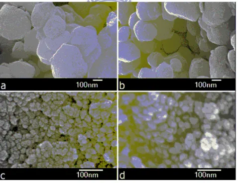
particles. --- 81 Figure 5.4 TEM images of nanocrystalline TiO2 core particles prepared (a) without an Al2O3
shell layer, (b) with a two-cycle-ALD Al2O3shell layer, (c) with a five-cycle-ALD
Al2O3shell layer, and (d) with a 10-cycle-ALD Al2O3shell layer. --- 86
Figure 5.5 The enlarged TEM images show the TiO2 core particles (a) without an Al2O3shell
layer, (b) with a one-cycle-ALD Al2O3shell layer, (c) with a five-cycle-ALD Al2O3
shell layer.--- 87 Figure 5.6 XPS spectra of the Ti 2p3/2peaks from the nanoporous TiO2 electrodes. --- 88
Figure 5.7 Coverages () of Al2O3 shell layers on TiO2 electrodes, obtained from XPS analyses.
The experimental data (crosses) match the corresponding theoretical curves from our C/S model. --- 90 Figure 5.8 Changes in the PCE and coverage, plotted with respect to the number of ALD
reaction cycles for Al2O3 shell layers on TiO2 electrodes.--- 92
Figure 6.1 XPS data for the (a) Ti 2p3/2 and (b) Al 2p core level photoelectron peaks from ALD Al2O3–coated TiO2 electrodes.--- 97
overlayer. Inset in (a) shows the high-magnification image of a selected area of the marked area. (b) TEM images of the marked area of a rutile TiO2particles (shown
in the inset) featuring a 10-cycle ALD Al2O3 overlayer. --- 98
Figure 6.3 Growth-per-cycle of the Al2O3overlayers as a function of the number of ALD
reaction cycles. --- 100 Figure 6.4 XRD spectra of the anatase electrode layer (a) and the rutile electrode layer (b) with respect to the number of ALD deposition cycles of the Al2O3overlayer. --- 102
Figure 6.5 Lattice volumes of TiO2 crystals in (a) the anatase and (b) in the rutile electrode
layers, plotted with respect to the number of ALD reaction cycles of the Al2O3
List of Symbols
I
nth: the signal intensities of the nth layer after the shell coating
Io
nth: the signal intensities of the nth layer before the shell coating
S*
: negative ion of dye
*
IB: the interfacial energy barrier height between N719 dye and
Al2O3a
: the thickness of each monolayer
a
: a fractional constant and is closely related to the size of the
region
A
A, core: projection area of the core particles in a layer
A
A, shell: projection area of the a shell-only-regions in a layer
ALD
: atomic-layer-deposition
x
: the strip angle
b
: the fractional constant for the shell-only region
C/S
: core/shell
CBM
: conduction band minimum
d
: the sample density (g/cm3)
D
: diameter of the bare core particles
C
M
: the number of atoms M (here is Al) adsorbed per unit surface
area per cycle
: the difference of work function between
over-layer
Al2O3and TiO
2h
: the thickness increment per cycle
: intensities of photoelectrons emitted from a single strip with
the shell layer
: intensities of photoelectrons emitted from a single strip without
the shell layer
I
bulk
: intensity of the photoelectrons from a strip of infinite length
DSSC
: dye-sensitized solar cell
E
: the e-beam energy (KeV)
RB
: charge recombination barrier height
eV
bi: built-in potential
: work function
FF
: fill factor
HOMO
: highest occupied molecular orbital
I
: total intensity (I) of photoelectrons emitted from the entire half
part of the circular plane with the shell layer
I
–/I
3–: negative ion of iodide/triiodide
: intensities of photoelectrons emitted from the substrate without
the thin film material
I
o: the intensity of photoelectrons from circular plane without the
shell layers
Io
total: total XPS signal intensity of the C/S structured thin film without
the shell layer
s
: intensities of photoelectrons emitted from the substrate with
the thin film material
I
total: total XPS signal intensity of the C/S structured thin film with the
shell layer
J
sc: short-circuit current
: the inelastic mean free path (IMFP) of electrons traveling in the
overlayer
core
: the IMFP of electrons traveling in the core particle
shell
: the inelastic mean free path (IMFP) of electrons traveling in the
shell layer
LUMO
: lowest unoccupied molecular orbital
M
: the molar mass of layer
M
: multi-layers Factor
M
W: molecular weight of the core or shell material
n
: the number of monolayers in an island
n
A: the number of the atoms in a molecule
N
a: Avogadro’s number
O
: the origin of the circle
P
: porosity
PCE
: the power conversion efficiency
: fractional coverage
island
: island coverage
S
+: positive ion of dye
SF
: sub-layer Factor
i
: interfacial energy
S
o: dye molecular
o
: surface energy of the overlayer
s
: surface energy of the substrate
st
: accumulated strain energy
t
x: thickness of the shell
VBM
: valence band maximum
V
oc: open-circuit voltage
V
V,core: volume fraction of the core particles in a layer
W
a: the width of a strip
WF
: work function
Chapter 1
Introduction
1.1 The Challenge for Photovoltaic Devices
Global energy consumption in 2030 is expected to rise 1.4 times than its present level [1]. It is anticipated the demand for fossil fuels will increase with economic growth of developing countries; however, the amount of main energy resources available for supply in the world will less than 130 years from present [2], as shown in Fig. 1.1. Based on the present rate of consumption, the remaining exploitable global resources, in term of years, show the expected period are 122, 42, and 60 years for coal, oil, and natural gas, respectively. Although new oil fields and mines will be discovered in the future, we cannot deny they are limited resources and need to be replaced by other more suitable energy resources. To the point, the supply of energy from the sun to the earth is estimated to be 3×1024 J/year, which is 10000 times more than the current global human consumption. That is, covering photovoltaic devices on only 0.1% of the earth’s surface with a conversion efficiency of 10% is sufficient for global needs at the present day [3].
The cost to generate the electric power is a key to alternative resources in the future. Table 1-1 shows the relative electric power cost generated by various resources [1]. The hydroelectric and wind power are clean and low-cost energy sources, but are restricted by the proper geography, weather and location. On the other hand, concerning global warming and pollution issues, solar cells are considered as the next generation energy resource, because it will be more cost-effective in the next two decades to generate the electric power than other energies, to support the continued growth of the global economy [4]. The Japanese research institute NEDO (New Energy Development Organization) and ANRE (Agency for Natural Resources and Energy, Government) expects that the power generation cost of new solar cells will reach 14 yen/KWh, lower than that of home-used electricity in 2020, and a power conversion efficiency of 20% [2]. Therefore, efforts are being focused on technologically developing new types of solar cells to reach higher efficiencies and lower production costs.
Table 1-1 The relative electric power cost generated by various resources [1].
Power source Units price of electric power generation
Hydroelectric 8.2 – 13.3 yen
Oil 10 – 17.3 yen
Natural gas 5.8 – 7.1 yen
Coal 5 –6.5yen
Nuclear 4.8 – 6.2 yen
Photovoltaic 49 yen
Wind 9 –14 yen
Recent concerns about the laborious, energy-consuming, and costly production of photovoltaic devices have accentuated the need for more efficient, dye-sensitized solar cells (DSSCs) [5]. As an emerging energy source, DSSC has the potential to become a third generation solar cell offering the following advantages [6]:
1. Low production cost and lower investment cost 2. Transparency and multi-color options
3. Flexibility 4. Lightweight
5. Feedstock availability to reach terawatt scale 6. Short energy payback time
7. Enhanced performance under diffuse light and higher temperatures 8. Capture light from all angles
9. Outperforms competitors for indoor applications
In addition to these advantages, the electric generation cost of DSSCs was regarded to be the lowest of photovoltaic devices in the 2020 to 2030 market evaluated by NEDO (New Energy Development Organization) and ANRE (Agency for Natural Resources and Energy, Japanese Government) [7], as shown in Fig. 1.2. The number of DSSCs research groups around the world is growing, indicating great opportunities of DSSCs to be a future alternative energy resource, as shown in Fig. 1.3 [6], a literature search illustrates the increase in the number of research papers and patents over the last several years.
Figure 1.2 The developing trend for the low cost of solar cells shows the DSSC as the main solar cell in 2020 to 2030 [7].
Figure 1.3 Number of (a) publications published per year, and (b) patents submitted, obtained from a simple and limited literature search using the keywords “dye-sensitized”and “solar” [6].
The commercial progress of DSSC in the near future is mainly hindered by two major problems: the rare ruthenium-based dye and the corrosive electrolyte [8]. However, some proponents of DSSCs expect these problems will be solved, especially for small-sized DSSCs, as international companies such as Samsung SDI, Corus, Sharp, DNP and 3G Solar are expected to produce products in the next two years [9]. As a result, the commercialization of DSSC will ideally occur in 2013. Presently, the application of DSSC, namely a Building Integrated Photovoltaic System (BIPV), will account for more than 50% of the DSSC market and portable electric chargers are expected to grow to 20% of the market. The annual production and growth rate of DSSC are expected to follow the trend shown in Fig. 1.4 [9]. The annual production may reach 2.6 GW in 2015 and the anticipated growth rate ranges between 100 and 520 % both the numbers showing the prosperous future of DSSC.
Figure 1.4 Dye-Sensitized Solar Cell(DSSC)'s annual production and growth rate forecasting [9].
1.3Enhancing the DSSC Efficiency with Core/Shell
Electrodes
A high efficient DSSC was developed in 1991 by using a nanoporous electrode to increase the dye/electrode interface, thus increasing the number of electrons transferred into the electrode [10]. Therefore, modifying the dye/electrode interface is a direct method to achieve higher efficiency in DSSC. One of the most efficient processes to enhance DSSC performance is to coat the porous electrodes with an ultra-thin oxide layer [11].
In literature, only three types of nanoporous electrodes (TiO2, SnO2 and ZnO) were
found to enhance the efficiency of DSSCs with core/shell structures. Figure 1.5 shows the performances of DSSCs with TiO2[12-23], SnO2 [24-31], ZnO [32-37]–core/shell electrodes
from 2001 to 2011. The most efficient electrode with shell layers, shown in Fig. 1.5(a) was a TiO electrode; in addition, SnO and ZnO core/shell electrodes produced more improvement
in efficiency of DSSCs. Al2O3 shells were the most commonly used layers in high efficient
TiO2–core/shell electrodes. Recently, the shell layers coated on TiO2 electrode by Atomic
Layer Deposition (ALD) increased the DSSC’s power conversion efficiency (PCE) by 14 to 80% indicating that ALD may be the ideal shell fabrication process for DSSCs, and hence further study is necessary [19, 21, 22].
Figure 1.5 (a) the efficiency of DSSCs and (b) the percent increase in PCE of DSSCs with TiO2[12-23], SnO2 [24-31], ZnO [32-37]–core/shell electrodes from 2001 to 2011. Asterisks
1.4 Objectives and Arrangements of the Study
Based on the aforementioned points, we chose atomic layer deposited Al2O3 over-layers
as the shell layers, on the nanoporous TiO2 electrodes of dye-sensitized solar cells (DSSCs).
Previous explanations for the improvement of DSSCs with the Al2O3 over-layers were based
solely on the assumptions made on the energy levels at core/shell interface and quality of the coating on the TiO2 electrodes which, consequently, were rarely accurate, because the
interfacial energy levels may change significantly due to chemical reaction and the coverage of shell layers may be decreased by the island growth. The future improvement of DSSCs will be determined, in part, by the extent of the understanding developed on the Al2O3/ TiO2
interface through the analysis of real energy levels and nano-structures.
To achieve a comprehensive study of the physical, chemical, and electrical properties of the Al2O3 over-layers, we studied three aspects of the ALD Al2O3/TiO2 electrodes: interfacial
energy levels, surface coverage, and growth mode. We examine a low-temperature ALD process for forming the Al2O3 barriers to achieve compatibility with low-temperature DSSCs
fabrication processes. The relation of interfacial energy level, surface coverage, and growth mode to power conversion efficiency (PCE) was investigated by using TEM, ultraviolet photoelectron spectroscopy (UPS), x-ray photoelectron spectroscopy (XPS), and reflective electron energy loss spectroscopy (REELS). The nano-structure and influence of ALD Al2O3
layers on nanoporous TiO2 electrodes in DSSCs were also studied using these
Chapter 1 introduces the motivation and objective of this study.
Chapter 2 reviews the literature concerning basic concept of solar energy, recent progress of DSSCs, characterization and previous studies of core/shell electrodes.
Chapter 3 describes the experimental method and analytic techniques.
Chapter 4 discusses the interfacial energy levels of Al2O3 films on TiO2 electrodes of
DSSCs. The related properties are also discussed.
Chapter 5 shows a calculated model that measures the coverage of the core/shell electrode of DSSCs from XPS signals. The model calculated the coverage from isolated spheres to muti-layers core/shell materials, which can evaluate the ideal PCE of DSSCs with the core/shell electrodes.
Chapter 6 discusses the growth modes of Al2O3deposited on TiO2electrodes of DSSCs.
Obtaining a comprehensive understandings of the influencing factors of the ALD Al2O3
deposited on TiO2electrodes of DSSCs was investigated.
Chapter 7 concludes the experimental results and suggests future work worthy for pursuing.
Chapter 2
Literature Review
This chapter reviews the properties of solar energy and power, development of dye-sensitized solar cells, and the characterization of core/ shell electrodes.
2.1 Solar Energy and Power Conversion Efficiency
The solar irradiance, also named as solar constant, is defined as the power density of sunlight outside the atmosphere of earth and is regarded as a constant, 1367 W/m2, by the World Radiometric Center (WRC) [38]. However, when sunlight reaches the earth’s surface, the solar radiation changed due to atmosphere effects (i.e., absorption and scattering), weather, latitude, time etc. The measurement of power conversion efficiency of solar cells is affected by many factors, hence, it is necessary to introduce the standard conditions to evaluate the power conversion efficiency of solar cells.
2.1.1 Air Mass
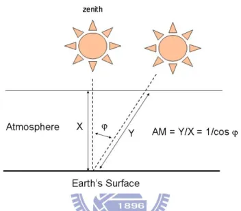
The maximum radiation strikes the earth’s surface when the sun is directly overhead, having the shortest path length through the atmosphere at clear skies. The path length is called the air mass (AM) and can be calculated by the equation AM = 1/cos, where is the zenith angle as shown in Fig. 2.1. The standard solar spectrum outside the earth’s atmosphere is called AM 0. The path length of standard solar spectrum used for efficiency measurements of solar cells is AM 1.5 G (global), given that = 48.19° [39]. Fig 2.2 presents the photon
The spectrum is normalized such that the integrated irradiance (i.e., the amount of radiant energy received from the sun per unit area) is 1000 W/m2. In the diagram, the maximum photocurrent is the current at short-circuit conditions for a solar cell device converting all incident photons below the absorption onset wavelength into electric current. For example, the maximum short-circuit current for a solar cell with an absorption onset of 700 nm is 20 mA/cm2.
Figure 2.1 Illustration of the path length of solar radiation and the zenith angle .
Figure 2.2 Photon flux of the AM 1.5 G spectrum at 1000 W/m2, and calculated accumulated photocurrent. (ASTM G173-03)
2.1.2 Power Conversion Efficiency
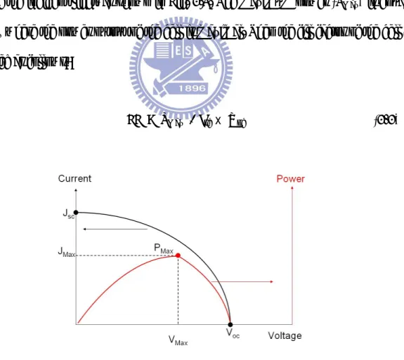
The power conversion efficiency (PCE, η) of the dye-sensitized cell is determined by the following equation [40]:
η= Jsc x Voc x FF / Is (2-1)
where the Jsc is the photocurrent density measured at short circuit, the Voc is open-circuit
photo-voltage, FF is the fill factor of the cell and equal to JMaxx VMax / Jscx Voc, and Is the
intensity of the incident light, as shown in Fig. 2.3. The maximum power (PMax) is equal to
JMax VMax where the power output of the cell is maximal. Then the fill factor of the cell can
be calculated as follows:
FF = PMax / Jsc x Voc (2-2)
2.1.3 Standard Measurement of PCE
Accurate efficiency measurement of a solar cell depends on the international standard reporting conditions (SRC) such as 100 mW/cm2 total irradiance, AM 1.5G reference spectrum, and 25 ℃ cell temperature [41]. The current AM 1.5G reference spectrum used by the international terrestrial photovoltaics community is from International Electrotechnical Commission (IEC) Standard 60904-3, as shown in Fig. 2.4, and American Society for Testing and Materials (ASTM) Standard G173-03. Typically, the irradiance incident on the solar cell is measured with a reference cell. The spectral error in the measured short-circuit current (JSC) of the solar cell is induced by the mismatch between the spectral
irradiance of the light source and the reference spectrum. In addition, the difference between the spectral responses of the reference detector and test cell needs to be corrected. Therefore, a correction for these errors should be applied. The errors can be expressed as a spectral mismatch correction factor (M) [41]:
M =
2 1 2 1 2 1 2 1 ) ( ) ( ) ( ) ( ) ( ) ( ) ( ) ( f Re f Re d S E d S E d S E d S E R S T T S R (2-3)where ERef() is the reference spectral irradiance, ES() is the source spectral irradiance, SR()
is the spectral responsivity of the reference cell, and ST() is the spectral responsivity of the
test cell, all of which are a function of wavelength (). The range of 1 and 2 in the above
Figure 2.4 Spectral irradiance for AM 1.5 G reference spectrum (IEC 60904-3) and the typical source irradiance of an Oriel 150 W solar simulator. Intensities of the spectra have been normalized to 100 mW/cm2 [41].
2.2 Developments in Dye-Sensitized Solar Cells
2.2.1 Evolution of Dye-Sensitized Solar Cells
In 1873, H. Vogel discovered the “dye sensitization” by adding some organic dyes into silver halide to enhance the green and red light absorption [42]. The silver halides used in photography are insensitive to visible light and have band gaps in the range of 2.7-3.2 eV, just as the TiO2 used in DSSCs. The dye-sensitized phenomenon was later explained as the
electron transfer from the organic dyes to the silver halide. What followed was the first sensitization of photo-electrode using a similar chemistry was performed in 1887 [43].
Research in the sensitization in solar cells then commenced [44-47] and showed cell conversion efficiencies below 1% in the following century.
The milestone of high-efficiency DSSCs was established by B. O’Regan and M. Grätzel in 1991 [10]. The cell construction with 7% solar power conversion efficiency composed of nano-crystalline TiO2 electrode and ruthenium complex dye is still used now in modern
DSSCs. The surface-area of the TiO2 film introduced was believed to induce the enormous
power conversion efficiency by loading larger amounts of dye and increasing light absorption. The great improvement achieved in their research was not only the introduction of the nano-crystalline TiO2 electrode, to achieve the enormous power conversion efficiency, but
also determining the main structure for the best-performing modern DSSCs. In recognition of this contribution, these types of DSSCs are generally referred as “Grätzel’s Cell”. In the decade after the original publication, the record efficiency for the Grätzel’s cell increased from 7.1% to 10%, however, in the subsequent decades the efficiency has only increased to 11.5% [48].
2.2.2 Operational Principles of Dye-Sensitized Solar Cells
The main operating principle of the DSSCs is presented in Fig. 2.5 [49]. From left to right, the cell consists of a transparent conductive oxide (TCO) substrate, normally doped SnO2 with fluorine on glass. A porous transparent semiconductor layer is coated onto the
substrate, normally 10-15 μm of ~20 nm TiO2 particles, which gives an internal surface
area of ~1000 cm2 per cm2 substrate. Dye molecules are absorbed onto the internal surface of this semiconductor to form approximately one monolayer. The typical dye is N719. The substrate is joined to a counter electrode, usually a few nanometers of platinum on another
TCO glass. A seal is formed around the cell, followed by injection of electrolyte through a hole which is subsequently sealed. So far all DSSCs have been based on an iodine/iodide electrolyte in organic solvent. A typical electrolyte consists of methoxyproprionitrile (MPN) with 0.6 M propylmethylimidazolium iodide, 0.1 M LiI, 0.1 M tert-butylpyridine, and 0.1 M iodine.
Figure 2.5 Energy band diagram of a typical DSSC employing an iodide/triiodide-based redox eletrolyte and N719 as a sensitizer dye [49].
As shown in Fig. 2.5, the sensitizer attached to the surface of a porous film absorbs the energy from sunlight (hv). The injection of electrons into the conduction band of the oxide is induced by the process of photo-excitation of the dye. Subsequently, the electron from electrolyte regenerates to the dye on the surface of porous films. The electrolyte contains the negative ion of iodide/triiodide (I–/I3–) couple as a redox couple. Reduction of positive ion of
ions (I3–). This prevents any significant increase of S+, which could recapture the conduction
band electron at the surface. The iodide is regenerated by the reduction of the triiodide ions at the counter-electrode, where the electrons are acquired from the external circuit through the Pt. The whole reaction can be represented by following processes.
Anode: So + hv → S* _Absorption S* → S+ + e-(TiO2) _Electron Injection
2S+ + 3I– → 2So + I3– _Regeneration
Cathode: I3– + 2e-(Pt) → 3I–
Cell: e-(Pt) + hv → e-(TiO2)
Where the So represents the dye, the S* indicates the negative ion of dye. Thus, the device is generating electricity from light without any permanent chemical transformations.
Recently, a second type of operating principle of the DSSCs was proposed [50-52]. As shown in Fig. 2.6, the type II DSSCs are based on direct electron injection from the ground state (HOMO) of the sensitizer (dye) into the conduction band of TiO2. Unlike the
conventional DSSCs, photoexcitation of the type II dye results in the direct electron injection from the ground state of the sensitizer into the conduction band of the TiO2, omitting the
charge transfer that electron jumping from the ground state to the excited state (LUMO) of dye and then injecting into the conduction band (ECB) of the TiO2. Noted that no
photoexcited dye states are involved in the type II DSSCs, in contrast to conventional DSSCs. Typical type II sensitizers are organic molecules composed of endiol ligands that form a chelating bond with an under coordinated tetrahedral Ti(IV) surface state [52].
Figure 2.6 Illustrations comparing the operational principles of a (a) conventional DSSC and (b) Type II DSSC [52].
2.2.3 Surface Area of the Nano-Crystalline Electrodes
The specific surface area of the nano-crystalline TiO2 structure is about 2000 times
larger than that of the bulk TiO2 structure [10] and directly increases both the light harvesting
area and dye-electrode interface enormously. Figure 2.7 compares the incident photon to charge carrier efficiency (ICPE) of dye-sensitized solar cell with flat electrode and nano-crystalline electrode, the improvement is about 600 times increase for the nano-crystalline electrode [5]. The incident-photon-to-current conversion efficiency is plotted as a function of wavelength with both flat electrode and nano-crystalline electrode. The IPCE value obtained with the single-crystal electrode is only 0.13% at 530 nm, where the value with the nanocrystalline electrode reaches 88% — more than 600 times greater.
Figure 2.7 Comparison of the incident wavelength to charge carrier efficiency (ICPE) of dye-sensitized solar cell with (a) flat electrode and (b) nano-crystalline electrode [5].
As mentioned above, there are many ways to improve the surface of porous electrodes to optimize the efficiency. One of the most successful methods is to coat the nano-crystalline electrode with a thin shell layer has been research over last decade. However, although many variants of the fabrication, including surface layers on nano-crystalline particles, have been studied, the lack of characterization limited the development in DSSCs with a core/shell electrode. For example, although a 0.2 nm thick shell layer can be deposited on a nano-crystalline or core/shell electrode, it is difficult to measure the surface coverage of this shell layer [53]. The following sections will discuss the problems in detail.
2.3 Core/Shell Electrodes in DSSCs
As shown in Fig 2.8, two core/shell structures have been developed to create the electrodes of DSSCs [54]. One includes the fabrication of nanoparticles and then forming a shell layer on the surface of nanoparticles. This leads to the formation of core/shell structured
nanoparticles to form the photoelectrode film (Fig 2.8a). However, such a structure creates an energy barrier not only at the nanoparticle/electrolyte interface but also between the individual core nanoparticles. In another structure, the photoelectrode film is composed of nanoparticles prepared prior to the deposition of shell layer, as show in Fig. 2.8(b). The latter structure is obviously beneficial to electron transport, it is a challenge to fabricate a shell layer in term of ideal uniformity of the shell material.
Figure 2.8 Core/shell structures used in DSSCs. (a) The shell layer is formed prior to the film deposition, (b) the shell layer is coated after the film deposition [54].
In this study, we defined the core/shell electrode like previous study [55] as the nanoporous inorganic semiconductor electrode that is covered with a shell of other metal oxide and coated after the film deposition. These electrodes can slow the recombination processes by the formation of an energy barrier at the TiO2 surface. The conduction band of
the shell should be higher than that of the core semiconductor to generate an energy barrier for the reaction of the electrons present in the core with the oxidized dye or the redox mediator in solution. Nevertheless, there exist the varying conclusions on the path of electron transfer through the shell layer.
2.3.1 Operational Principles of Core/Shell Electrodes
The first core/shell electrode was developed by A. Zaban et al. in 2000 [11]. They reported the fabrication of a TiO2/Nb2O5 nanoporous electrode, which improved the
performance of dye sensitized solar cells by more than 35%. In the mechanism described as the illumination of a DSSC, an electron is injected from the dye into the TiO2 film followed
by a hole transfer to the electrolyte. The injected electrons must cross the TiO2 film and reach
the conducting substrate, while the oxidized ions diffuse towards the back electrode, where they are re-reduced. The porous geometry that permits the presence of the electrolyte through the entire electrode provides a high surface area for recombination between the injected electrons and the holes in solution. In the absence of an energy barrier at the electrode–electrolyte interface, the rate of this recombination process may be very high depending on the properties of the hole carrier. As illustrated in Fig. 2.9, the energy level differences form an energy barrier at the electrode–electrolyte interface, which can reduce the rate of recombination processes of the photoinjected electrons. A comparison of two similar DSSCs that differ only in their nanoporous electrode, shows that the core/shell electrode is superior to the standard one with respect to all cell parameters. This demonstrated superiority, measured from many cells results in a 35% increase of the overall conversion efficiency.
Figure 2.9 A schematic view of the new nanoporous electrode which consists of a nanoporous TiO2 matrix covered with a thin layer of Nb2O5 [11].
The second mechanism suggested by E. Palomares [14,15], where the conformal growth of an overlayer of Al2O3 on a nanocrystalline TiO2 film, is shown to result in a 4-fold
retardation of interfacial charge recombination, and a 30% improvement in photovoltaic device efficiency. The main charge-transfer events that take place at the TiO2/dye/electrolyte
interface are depicted in Fig. 2.10. Visible light is absorbed (1) by the sensitizer dye. Electron injection (2) from the excited state of the dye into the conduction band of the TiO2 by
tunneling effect is followed by the subsequent regeneration of the dye by I–/I3– red/ox couple
(4). Efficient operation of the DSSC device relies upon the reduction of the possible recombination pathways occurring at the TiO2/dye/electrolyte interface, allowing efficient
charge transport through the TiO2 film and electrolyte and subsequent charge collection at
the device contacts. There are two possible recombination losses to consider. The injected electrons may recombine either with oxidized dye molecules (3) or with the oxidized redox couple (5).
Figure 2.10 Illustration of the interfacial charge-transfer processes occurring at the nanostructure TiO2/dye/electrolyte interface of DSSC [14,15].
The difference between these two mechanisms can be seen at the path (2) of electron transfer. The first mechanism claimed electron injection (2) from the dye into TiO2 without
any energy barriers, but the second mechanism assumed electron injection (2) from dye into TiO2 by tunneling effect. This understanding is based on the assumption of that ultra-thin
over-layers maintain the same energy levels after coating on the TiO2 electrodes as in the
bulk structure; consequently, the energy diagrams of DSSCs with Al2O3/ TiO2 interface
structures have been determined mostly by inserting the energy data from bulk material and assuming the vacuum levels of all of the layers are equal.
In 2002, Diamand et al. used SrTiO3as a shell layer to coat on the TiO2 electrode [55].
They found that SrTiO3layer shifted the conduction band of the TiO2(ECB0) in the negative
direction, rather than formed an energy barrier at the TiO2 surface, as shown in Fig. 2.11.
This type of photoanode modification cannot suppress the back recombination rate as a function of the electron density, but can suppress the back recombination as a function of the applied potential. As a result, the forming “surface dipole” reduced Jsc slightly and significantly increased the Voc and the devices conversion efficiency was improved by 15.3%.
As shown in Fig. 2.11(b), the formation of a potential step subjected to the surface dipole shifted the conduction band of TiO2 in the negative direction.
Figure 2.11 Energy diagram representing the movement of (a) the TiO2conduction band by
the SrTiO3 coating and (b) the effect of the band shift at applied potential indicated the
coated system is more resistive than the bare electrode [55].
The core/shell electrode has also been used in the type II DSSC [52]. Figure 2.12 shows the operation of the SrTiO3 barrier layer as a barrier of recombination in the type II DSSC
using catehol as a dye; therefore, the cell is named a catechol-sensitized type II DSSCs (CSSCs). The SrTiO3’s conduction band is higher than the conduction band of TiO2 by 0.2
eV, forming an energy barrier between the TiO2 and the catechol. Due to excitation, an
electron is injected from the HOMO level of the catechol molecule into the conduction band of the SrTiO3. The energy difference between the SrTiO3 and TiO2 conduction band edges
creates a tendency for the electron transfers from the SrTiO3layer to the TiO2 core, resulting
in the reduction of the back electron transfers to the oxidized catechol compared to the uncoated TiO2 particles.
Figure 2.12 Schematic drawing of a CSSC with a SrTiO3 barrier layer (left). The band
diagram shows the different electron-transfer processes (right) [52].
Another method to improve electron injection and suppress electron recombination in core/shell electrodes is by reducing the surface state sites of electrode via passivation [56,57]. Figure 2.13 shows the band diagrams before passivation (right) and after passivation (left). Passivation induces a larger band gap that could further suppress electron recombination. According to previous studies [58, 59], 3–10 nm PbS particles which filled the surface states of TiO2electrode effectively and improved power conversion efficiency by 20%. The similar
Figure 2.13 The band diagrams show the band gap (Eg) before passivation (right) and after passivation (left). A larger band gap could further suppress more electron recombination [56,57].
2.3.2 The Materials of Electrodes with Shell Structure
Generally, materials for high-efficient electrodes should satisfy the two important conditions: a) ease in fabricating the larger surface areas, b) a band structure compatible with that of the dye, and c) high stability to the corrosive electrolyte. The compatible band structure can be expressed as shown in Fig. 2.14, with the band positions of some photo-semiconductors in contact with electrolyte at PH 1 [5]. The conduction band minimus (CBM) of electrodes should be similar to TiO2 or near the zero energy of the normal
hydrogen electrode (NHE), since the CBM of dye is just about 0.4 eV higher than the zero energy [53]. Therefore, combined with condition (a) and (c), three types of electrodes (TiO2,
SnO2 and ZnO) were found, in the literature, to enhance the efficiency of DSSCs by the shell,
Figure 2.14 The band positions of photo-semiconductors in contact with electrolyte at PH 1 [5].
2.3.2.1 TiO
2Electrodes with Shell Structures
Table 2-1 summarizes the performances of DSSCs with TiO2-core/shell electrodes with
PCE greater than or equal to 5.0 %, from 2001 to 2011 [12-23]. Al2O3 is the most popular
shell material with many researchers improving the PCE of DSSCs by 14 to 35 %. A ZnO shell layer increased the PCE to 9.8% which is the highest performance in the table; however, there is a controversy on this study due to the later studies reported only 2.29 to 4.51% PCE for DSSCs with ZnO shell layers [61, 62]. The shell layers fabricated by Atomic Layer
Deposition (ALD) which increase the DSSC’s PCE by 14 to 80% indicated the ALD may be the ideal shell fabrication process for DSSCs and the further study is necessary.
Table 2-1 Summary of the performances of DSSCs with TiO2-core/shell electrodes for PCE
values greater than or equal to 5.0 % from previous studies [12-23].
Reference Year Electrode Shell layer
Shell fabricated process PCE (%) Percent increase in PCE (%) [12] 2001 Nano-Porous TiO2 Nb2O5 Sol-gel 5.0 35 [13] 2001 Nano-Porous TiO2 ZnO Hydrothermo method 9.8 27.3 [14] 2002 Nano-Porous TiO2 Al2O3 Sol-gel 5.0 30 [15] 2003 Nano-Porous TiO2 Al2O3 Sol-gel 5.6 35 [16] 2006 Nano-Porous TiO2 CaCO3 Dip-coating 7.9 14.5 [17] 2008 Nano-Porous TiO2 MgO Sputtering 7.5 17.4 [18] 2009 Nano-Porous TiO2 CaO Evaporation 6.0 15.1 [19] 2009 Nano-Porous TiO2 Al2O3 Atomic Layer Deposition 7.8 14 [20] 2010 Nano-Porous TiO2 HfO2 Atomic Layer Deposition 7.1 69
[21] 2010 Nano-Porous TiO2 Al2O3 Atomic Layer Deposition 8.4 35 [22] 2010 Nano-Porous TiO2 SiO2 Atomic Layer Deposition 7.2 80 [23] 2010 Nano-Porous TiO2 Ba(NO3)2 Dipping/sintering 6.7 28
In 2004, A. Zaban found a relation between Voc change and the isoelectric point (IEP) of
shell materials on TiO2, that is, the Voc is roughly proportional to the isoelectric point, as
shown in Fig. 2.15 [55]. He proposed that oxides such as ZnO, SrTiO3, ZrO2 and Al2O3 with
isoelectric points higher than that of the TiO2, created a positive charge on surface, leading to
an increase in the open circuit voltage; however, the Al2O3shows some different trend in the
figure that might be attributed to the formation of surface dipole layer on the Al2O3 shell. A
surface dipole layer was created toward the TiO2, leading to an increase in the open circuit
voltage of the cells; however, a decrease in the photocurrent was observed. This indicates the formation of a dipole layer might accelerate the electron recombination. It should be noted that the observed photocurrent is the difference between the forward photocurrent and the photocurrent caused by the back recombination. Therefore, for the TiO2-core/ Al2O3-shell
Figure 2.15 A relation between Voc change and the isoelectric point (IEP) of shell materials
on TiO2[55].
2.3.2.2 SnO
2Electrodes with Shell Structure
Table 2-2 lists the performances of DSSCs with SnO2-core/shell electrodes for PCE
fabricated from 2001 to 2011 [24~ 31]. The SnO2 core/shell electrodes produced much lower
PCE than the TiO2 core/shell electrodes. The Al2O3, ZnO, TiO2 are the most popular shell
materials used for SnO2 electrodes which improved the PCE of DSSCs by 166 to 460 %. The
Nb2O5 shell layer increased the PCE to 5.48 % which is the highest performance of all shell
layers. Recently, the shell layers fabricated by Atomic Layer Deposition (ALD) increased the DSSC’s PCE by 386 %, indicating the ALD may be the ideal shell fabricated process for SnO2 electrodes and the further study maybe necessary.
Table 2-2 Summary of the performances of DSSCs with SnO2-core/shell electrodes [24-31].
Reference Year Electrode Shell layer
Shell fabricated process PCE (%) Percent increase in PCE (%) [24] 2001 Micro-Porous SnO2 Nano-Particle Al2O3 Dip-coating 3.2 166 [25] 2002 Nano-Porous SnO2 ZnO Mixing 5.2 333 [26] 2004 Nano-Porous SnO2 ZnO Mixing 3.5 439 [27] 2005 Nano-Porous SnO2 Nano-Particle TiO2/Al2O3 Dip-coating 2.85 285 [28] 2010 Nano-Porous SnO2 Nano-Particle TiO2 Dip-coating 3.8 245 [29] 2010 Nano-Porous SnO2
TiO2/MgO Dip-coating 2.8 460
[30] 2010 Nano-Porous SnO2 Al2O3 Atomic Layer Deposition 3.7 386 [31] 2011 Nano-Porous SnO2 Nb2O5 Dip-coating 5.48 220
In 2002, M. Grätzel [25] coated different oxides on SnO2 electrode and summarized the
performances of DSSCs as shown in Table 2-3, listing the data that also roughly obey the relationship between the isoelectric point and Voc. In addition, the surface of the oxide
coating was more basic than SnO2, which increased dye attachment and resulted in the
was about a few angstroms, suggesting that electron transfer occurs from dye to SnO2 by the
tunneling effect. Different coating methods for SnO2 nano-crystals with a thin layer of an
insulating oxide may result in different efficiencies. On the other hand, the shell coverage and thicknesses in the table indicated these two factors are important issues in affecting the efficiency of the DSSCs, but a comprehensive study is still lacking.
Table 2-3 Summary of the performances of DSSCs with SnO2-core/shell electrodes, from
reference [25].
2.3.2.3 ZnO Electrodes with Shell Structure
Table 2-4 lists the performances of DSSCs with ZnO-core/shell electrodes for PCE from 2001 to 2011 [32-37]. The ZnO-core/shell electrodes received better PCE than the SnO2-core/shell electrodes but lower than TiO2. The TiO2, SiO2 are most popular shell
materials used for ZnO electrodes to improve the PCE of DSSCs by 4 to 1012 %. The atomic-layer-deposited TiO2 shell layer increased the PCE to 6.3 % which is the highest
the ideal shell fabricated process for ZnO electrode and the further study maybe necessary.
Table 2-4. Summary of the performances of DSSCs with ZnO-core/shell electrodes [32-37].
Reference Year Electrode Shell layer
Shell fabricated process PCE (%) Percent increase in PCE (%) [32] 2005 Nano-Porous
ZnO TiO2 Dip-coating 1.78 1012
[33] 2007 Nano-Porous
ZnO SiO2 Sol-gel 5.2 900
[34] 2008 Nano-Porous
ZnO TiO2 Dip-coating 1.02 100
[35] 2010 Nano-Porous
ZnO SiO2 Sol-gel 4.51 4
[36] 2010 Nano-Porous ZnO TiO2 Atomic Layer Deposition 6.3 21.1 [37] 2011 Nano-Porous ZnO Nb2O5 Dip-coating 5.2 4.4
The ZnO electrode may not be an appropriate material to be coated with high efficient shell layers because its isoelectric point is quite high (see Fig. 2.15); however, the band structure of ZnO is similar to TiO2, explaining the DSSC’s performance enhancement by the
surface passivation of SiO2 or the efficient electron transportation of TiO2 shell layer. It
should be noted that ZnO and SiO2 are also two of the best shell layers applied on TiO2
electrode, as can be seen in Table 2-1. On the other hand, recently, the advanced structure of porous ZnO electrode was referred as the submicrometer-sized ZnO nanocrystallite
aggregates, which can enhance light scattering and efficiency of DSSCs without decreasing the surface area of electrodes for dye adsorption or TiO2 shell [36], as shown in Fig. 2.16.
This shows the ZnO electrodes with nanocrystallite aggregates might have the potential to improve the efficiency with shell layers.
Figure 2.16. Illustrations showing (a) ZnO aggregates with dye molecules, (b) ZnO nanocrystallites withg micropores, (c) thin ALD-TiO2 layer on ZnO nanocrystallites, (d)
enlarged schematic of (c), and (e) SEM of the aggregates of ZnO nanocrystallites, (f) SEM of the aggregates of ZnO nanocrystallites coated with thin TiO2 layer [36].
2.3.2.4 Atomic Layer Deposited Al
2O
3Shells
As there is a lot of interest and work in efficiency enhancement, the power conversion efficiency (PCE) of DSSCs based on nanoporous TiO electrodes has been consistently
increased by 14-35% using Al2O3 over-layers [14-15, 19, 21]. Optimization of the
Al2O3/TiO2 interface in DSSCs was carried out by different coating procedures, which have
relied so far on sol-gel or solution processes that provide the capability of infiltrating porous structures thereby ensuring good coverage of the surface of the nanoporous electrode. The sol-gel or solution processes require a sintering step at 450-500 ºC to achieve good quality and, hence, has limited compatibility with low-temperature fabrication processes, such as those for making plastic-based flexible DSSCs [64]. Low-temperature (100 ºC) sol-gel Al2O3
layers have been demonstrated on flexible DSSCs by Haque et al [65], however, the improvement provided was not as significant as that achieved by the high-temperature sol-gel process. Besides the temperature constraints of the typical sol-gel process, the thickness of the sol-gel films can only be altered with a resolution of ~1 nm [14, 66], which is too coarse for adjusting the optimal thickness of the Al2O3 layers. Atomic layer deposition (ALD) was
regarded as an ideal method for forming a well structured Al2O3/TiO2 interface, because it
offers high conformability ensuring uniform deposition onto the entire surfaces of nanoporous structures [67], low deposition temperatures (down to 33 ºC for Al2O3) [68], and
high resolution (~0.1 nm for Al2O3) for enhanced control of the film thickness [69, 70].
Hence, ALD provides a significant opportunity to enhance the PCE by providing advanced Al2O3 over-layers on TiO2 electrodes of DSSCs. The chemical reactions of ALD Al2O3
overlayers on a titania substrate can be seen in reference [71] or in chapter 3.2.
One advanced report on enhancing the PCE of DSSCs by ~14% with atomic layer deposited Al2O3 over-layers on TiO2 electrodes was provided in 2009 [19]. The optimal
thickness for the ALD barriers was produced by 1 cycle of ALD (0.1 nm in nominal thickness), which resulted in an average increase in PCE of 14% among the 11 devices tested, with the highest achieved PCE being 7.82%. The TiO2 electrode was 6 m in diameter and
![Table 1-1 The relative electric power cost generated by various resources [1].](https://thumb-ap.123doks.com/thumbv2/9libinfo/8240629.171317/23.892.214.715.769.1019/table-relative-electric-power-cost-generated-various-resources.webp)
![Figure 2.5 Energy band diagram of a typical DSSC employing an iodide/triiodide-based redox eletrolyte and N719 as a sensitizer dye [49].](https://thumb-ap.123doks.com/thumbv2/9libinfo/8240629.171317/37.892.202.715.319.727/figure-energy-diagram-typical-employing-triiodide-eletrolyte-sensitizer.webp)
![Figure 2.7 Comparison of the incident wavelength to charge carrier efficiency (ICPE) of dye-sensitized solar cell with (a) flat electrode and (b) nano-crystalline electrode [5].](https://thumb-ap.123doks.com/thumbv2/9libinfo/8240629.171317/40.892.139.802.109.402/comparison-incident-wavelength-efficiency-sensitized-electrode-crystalline-electrode.webp)
![Figure 2.10 Illustration of the interfacial charge-transfer processes occurring at the nanostructure TiO 2 /dye/electrolyte interface of DSSC [14,15]](https://thumb-ap.123doks.com/thumbv2/9libinfo/8240629.171317/43.892.151.787.533.1013/illustration-interfacial-transfer-processes-occurring-nanostructure-electrolyte-interface.webp)
![Table 2-2 Summary of the performances of DSSCs with SnO 2 -core/shell electrodes [24-31].](https://thumb-ap.123doks.com/thumbv2/9libinfo/8240629.171317/52.892.124.813.162.880/table-summary-performances-dsscs-sno-core-shell-electrodes.webp)
![Table 2-3 Summary of the performances of DSSCs with SnO 2 -core/shell electrodes, from reference [25].](https://thumb-ap.123doks.com/thumbv2/9libinfo/8240629.171317/53.892.131.806.438.737/table-summary-performances-dsscs-sno-shell-electrodes-reference.webp)
![Table 2-4. Summary of the performances of DSSCs with ZnO-core/shell electrodes [32-37].](https://thumb-ap.123doks.com/thumbv2/9libinfo/8240629.171317/54.892.121.817.258.830/table-summary-performances-dsscs-zno-core-shell-electrodes.webp)