國 立 交 通 大 學
電子工程學系 電子研究所
碩 士 論 文
應用於序列傳輸系統
之 10-Gbps 離散時間適應性等化器
A 10-Gbps Discrete-Time Adaptive Equalizer
for Serial Link System
研 究 生:許馥淳
指導教授:周世傑 博士
應用於序列傳輸系統之 10-Gbps 離散時間適應性等化器
A 10-Gbps Discrete-Time Adaptive Equalizer
for Serial Link System
研 究 生: 許馥淳
Student:Fu-Chun Hsu
指導教授: 周世傑 博士
Advisor:Prof. Shyh-Jye Jou
國 立 交 通 大 學
電子工程學系 電子研究所碩士班
碩 士 論 文
A Thesis
Submitted to Department of Electronics Engineering & Institute of Electronics
College of Electrical and Computer Engineering National Chiao Tung University
in Partial Fulfillment of the Requirements for the Degree of Master of Science
in
Electronics Engineering September 2009
Hsinchu, Taiwan, Republic of China
應用於序列傳輸系統之 10-Gbps 離散時間適應性等化器
研究生:許馥淳
指導教授:周世傑博士
國立交通大學
電子工程學系電子研究所碩士班
摘 要
隨著積體電路製程技術的進步,晶片的操作速度變得越來越快,晶片間傳遞 資料的高頻寬輸出入介面愈來愈重要。各種高速序列傳輸技術廣泛的使用在許多 高效能的電子產品中。為了讓訊號經過傳輸通道衰減後可以維持一定的品質,等 化器在高速序列傳輸系統中扮演了重要的角色。而由於通道的特性會因為環境而 改變,適應性等化器較適合於長時間的使用。 在本論文中,我們提出了一個操作在 10 Gbps 2-tap 的離散時間適應性決策 回授等化器。在等化器系統的前端,我們設計了一個可變增益的放大器,來調整 輸入訊號的振幅到下一級電路接受的範圍。另外,我們設計了一個高速、電流模 式的加法器,用來消除 post-cursor ISI。接著,我們提出一個叫跳躍式係數更 新的方案,還有一個混合訊號的積分器,來實現係數更新的機制。跳躍式係數更 新方案可以藉由降低係數更新的速度,來減少功率的消耗。混合訊號積分器是由 一個四位元的上數下數計數器和一個電荷幫浦組成,用來獲取更好的輸出表現和 較小的面積。我們使用了延遲 sign-sign LMS 演算法來做係數的收斂。提出的等化器是用 65 奈米互補式金氧半導體製程來設計。模擬結果位於等化器輸出的信 號眼圖可以開至正負 200 mV,而緩衝器的輸出端可以將信號眼圖張開到規格所 定的正負 300 mV。在等化器輸出的峰對峰值抖動大約 31ps。而係數的收斂時間 約為 20000 個位元時間。電路總面積為510 × 510 μm2,而核心電路面積是115 × 95 μm2。在 1.2V 的操作電壓下,電路總功率為40.63 mW,其中等化器系統佔了 11.18 mW。
A 10-Gbps Discrete-Time Adaptive Equalizer
for Serial Link System
Student: Fu-Chun Hsu
Advisor: Prof. Shyh-Jye Jou
Department of Electronics Engineering
Institute of Electronics
National Chiao Tung University
ABSTRACT
With the advance of integrated circuits (IC) fabrication technology, the operation speed of chips is becoming faster and faster. High-bandwidth I/Os have found a great demand for transferring data between chips. Many high-speed serial link transmission technologies are developed and are widely used for high performance modern electronic products. In order to maintain the signal quality that will be attenuated by communication channel, the equalizer becomes an important component in the high-speed serial link system. Since the characteristics of channel may vary due to the environment, adaptive equalizer is much preferable for long-time usage.
In this thesis, we propose a 2-tap discrete-time adaptive decision-feedback equalizer that operates at 10 Gbps. We design a variable gain amplifier in the front of the proposed equalizer system to adjust the swing of input signal in the range for the following stage. A high-speed current-mode summer is designed to cancel the
post-cursor ISI. A coefficient updating scheme called hopping and a mixed-signal integrator are presented to realize the mechanism of coefficients adaptation. The hopping update scheme can reduce the power consumption by slowing down the operation speed in the coefficients adaptation. The mixed-signal integrator consists of a 4-bit up/down counter and a charge pump to acquire a good performance and small area. We use the delayed sign-sign LMS algorithm to do the convergence of coefficients. The proposed equalizer is designed in a 65-nm CMOS technology. The simulation result shows that the data eye in the output of equalizer is about ±200 mVpp, and the data eye in the output of buffer stage can reach ±300 mVpp that meets
our specification. The peak-to-peak jitter at the equalizer output is about 31ps. The convergence time of coefficients is about 20000 bits time. Total area of our proposed equalizer including pads is 510 × 510 μm2 while the core area is 115 × 95 μm2. The total power consumption is 40.63 mW while the equalizer system consumes 11.18 mW under 1.2V power supply.
誌 謝
終於到了論文完成的這一天,真的很開心。首先要感謝我的指導教授周世傑 老師,提供非常完善的研究環境與資源,另外在每次的 meeting 報告時所給予的 糾正及建議,都讓我獲益良多,研究也才能這麼順利。因為老師的諄諄教誨,讓 我在研究的領域裡,不斷的精進,也才能完成論文,非常感謝老師。 再來要感謝育群學長,在我研究過程中,給予我相當大的幫助,尤其是觀念 的解釋,還有研究細節的指導。由於學長的幫助,我的研究才不至於停滯不前, 非常謝謝學長。 接著要感謝實驗室的學長跟同學們:jackie、mike、小胖、大大、小肥、明 賢、志宇、代暘、明銓,大家一起在實驗室度過很多快樂時光,一起研究、互相 學習。另外還有學弟妹:以樂、銘謙、祥譽、雅雪、為凱。有了大家,研究的日 子很快就在歡樂聲中度過了。 最後要感謝我的父母,總是給予我關心和鼓勵,讓我更可以全力專心在研究 上,最終也才能完成這個學位與論文。因為你們的栽培,才有今日的我,謝謝你 們。Contents
Chapter 1 Introduction ...1
1.1 The Challenge for High-Speed Serial Link...1
1.2 Motivation and Challenge of High-Speed Equalizer ...3
1.3 Thesis Organization ...3
Chapter 2 Overview of Equalizer for Serial Link System ...5
2.1 Overview of Serial Link System...5
2.2 Basic Concepts...7
2.2.1 NRZ Data ...7
2.2.2 Pseudo-Random Binary Sequence...8
2.2.3 Intersymbol Interference...9
2.2.4 Eye Diagram ...11
2.2.5 Bit Error Rate...13
2.3 Channel Model...15
Chapter 3 Equalization Basis ...23
3.1 Continuous-Time Equalization ...23
3.2 Discrete-Time Equalization ...28
3.2.1 Pre-and Post-Cursor ISI ...28
3.2.2 Feed-Forward Equalizer...30
3.2.3 Decision-Feedback Equalizer ...32
3.3 Sign-Sign LMS Algorithm...37
Chapter 4 Discrete-Time Adaptive Decision-Feedback Equalizer ...41
4.1 DT-ADFE Architecture ...41
4.2.1 Hopping Coefficients Update Scheme...43
4.2.2 Mixed-Signal Integrator...44
4.3 Behavioral Simulation Results...48
Chapter 5 A 10-Gb/s Adaptive Decision-Feedback Equalizer Implementation...58
5.1 System Description ...58
5.2 Circuit Design ...60
5.2.1 Variable Gain Amplifier...60
5.2.2 Current-Mode Summer ...63
5.2.3 Current-Steering Latch...65
5.2.4 Up-Down Counter...67
5.2.5 Charge Pump...69
5.3 Simulation Results and Layout Implementation...71
5.4 Measurement Environment Setup...76
Chapter 6 Conclusions and Future Work ...78
List of Figures
Figure 1.1 A typical serial link block diagram. ...1
Figure 1.2 Illustration of ISI phenomenon.a (a) An impulse and its response. (b) A series of impulse and their response. ...2
Figure 2.1 Signaling in a typical serial link. ...5
Figure 2.2 Typical serial link with equalizers. ...7
Figure 2.3 Block diagram of equalizer in receiver side. ...7
Figure 2.4 NRZ and RZ data...8
Figure 2.5 Random binary sequence...8
Figure 2.6 Pseudo-random binary sequence. ...9
Figure 2.7 (a) A low-pass filter. (b) Effect of low-pass filtering on random data...10
Figure 2.8 Response of long run passes a moderate limited bandwidth channel...11
Figure 2.9 An illustration of eye diagram construction. (a) input and output waveform. (b) eye diagram. ...12
Figure 2.10 PDF of signal plus noise...13
Figure 2.11 LC model of a transmission line. ...17
Figure 2.12 Lumped RLGC model of transmission line...18
Figure 2.13 Frequency response of 6-inch backplane channel. ...20
Figure 2.14 Impulse response of 6-inch backplane channel. ...20
Figure 2.15 Frequency response of channel model in HSPICE...21
Figure 2.16 Error in curve fitting between MATLAB and HSPICE...22
Figure 3.1 Channel response and equalizer response. ...24
Figure 3.2 Frequency response of continuous-time equalizers...24
Figure 3.3 Continuous-time passive equalizer. ...25
Figure 3.5 Discrete-time representation of pre- and post-cursor ISI. ...29
Figure 3.6 A linear feed-forward equalizer (FFE) topology...30
Figure 3.7 A parallelized analog FIR equalizer...32
Figure 3.8 Typical block diagram of DFE with one tap...33
Figure 3.9 Look-ahead one-tap DFE...35
Figure 3.10 Half-rate look-ahead DFE...36
Figure 3.11 N-tap FIR Wiener filter. ...37
Figure 3.12 An adaptive one-tap DFE. ...40
Figure 4.1 DT-ADFE architecture...42
Figure 4.2 Discrete-time integrators, (a) n-bit counter and m-bit DAC. (b) cascaded counters and m-bit DAC. (c) k-bit counter and analog integrator. ...45
Figure 4.3 Mixed-signal integrator...46
Figure 4.4 (a) DFE coefficients and (b) error of hopping update scheme with data rate. ...49
Figure 4.5 (a) DFE coefficients and (b) error of hopping update scheme with 1/4 data rate...49
Figure 4.6 (a) DFE coefficients and (b) error of hopping update scheme with 1/8 data rate...50
Figure 4.7 (a) DFE coefficients and (b) error of hopping update scheme with 1/16 data rate...50
Figure 4.8 Histogram of error. ...51
Figure 4.9 (a) DFE coefficients and (b) error of hopping update scheme with data rate and 3-bit up/down counter. ...52
Figure 4.10 (a) DFE coefficients and (b) error of hopping update scheme with 1/4 data rate and 3-bit up/down counter...53
data rate and 3-bit up/down counter...53
Figure 4.12 (a) DFE coefficients and (b) error of hopping update scheme with 1/16 data rate and 3-bit up/down counter...54
Figure 4.13 (a) DFE coefficients and (b) error of hopping update scheme with data rate and 4-bit up/down counter. ...55
Figure 4.14 (a) DFE coefficients and (b) error of hopping update scheme with 1/4 data rate and 4-bit up/down counter...56
Figure 4.15 (a) DFE coefficients and (b) error of hopping update scheme with 1/8 data rate and 4-bit up/down counter...56
Figure 4.16 (a) DFE coefficients and (b) error of hopping update scheme with 1/16 data rate and 4-bit up/down counter...57
Figure 5.1 Circuit architecture of our equalizer system...59
Figure 5.2 Sign-Sign LMS engine. ...60
Figure 5.3 VGA cell. ...61
Figure 5.4 Half circuit of VGA cell. ...61
Figure 5.5 Frequency response of cascaded 2 VGA cells with different Vg...62
Figure 5.6 Current-mode summer. ...64
Figure 5.7 Current-steering latch, (a) schematic and (b) timing waveform...66
Figure 5.8 Block diagram of 4-bit up/down counter...68
Figure 5.9 Simulated result of 4-bit up/down counter. ...69
Figure 5.10 Schematic of the charge pump...70
Figure 5.11 Layout view of the charge pump. ...71
Figure 5.12 Simulated coefficient voltages...72
Figure 5.13 Simulated eye diagram. (a) channel output. (b) equalizer summation output. (c) buffer output...73
equalizer system...74
List of Tables
Table 1.1 Industrial data-rate standards of high-speed serial link...2
Table 2.1 BERs for different confidence intervals. ...15
Table 4.1 MSE and convergence time for hopping update scheme at four different frequencies………… ...51
Table 4.2 MSE and convergence time for 3-bit Up/Down counter with hopping update scheme at four different frequencies. ...54
Table 4.3 MSE and convergence time for 4-bit Up/Down counter with hopping update scheme at four different frequencies. ...57
Table 5.1 Summary of the proposed equalizer ...75
Table 5.2 Comparison with other works ...76
Chapter 1 Introduction
Chapter 1
Introduction
1.1 The Challenge for High-Speed Serial Link
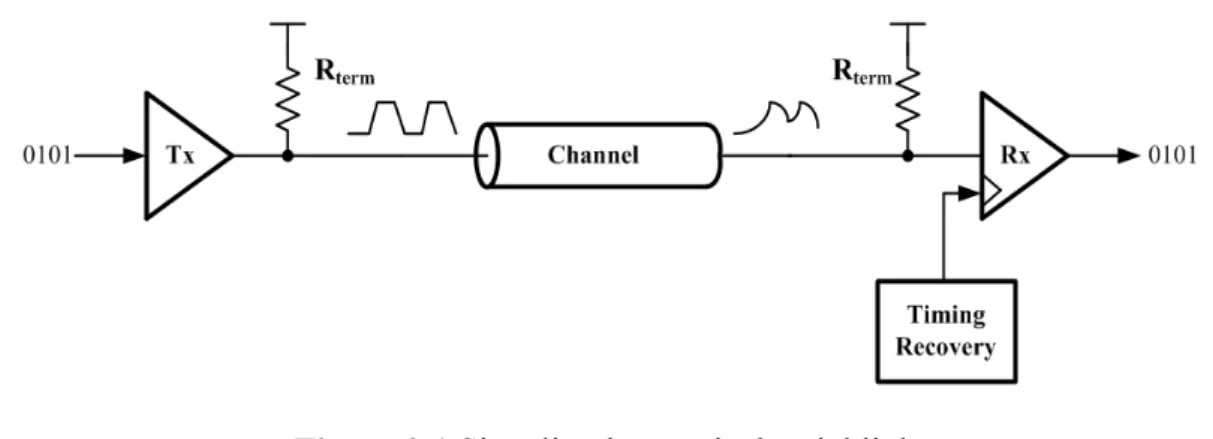
With the advances in integrated circuits (IC) fabrication technology, the speed of on-chip data processing as well as the integration level will continue to increase. High-speed inputs and outputs (I/Os) become an important role to transfer large amounts of data in many applications, including computer-to-peripheral connections, local-area networks, inter-chip communications and so on. In modern interconnect systems, high-speed serial links have replaced parallel data buses and become the dominant I/Os for data transmission. A typical serial link block diagram is shown in Fig. 1.1. The serial link is composed of three primary components: a transmitter, a channel and a receiver. We will discuss these three blocks in chapter 2.
Figure 1.1 A typical serial link block diagram.
Table 1.11 shows the data rates of industrial standards about high-speed serial links. As the speed of data rates increase, the design of high-speed serial links becomes a big challenge for maintaining signal integrity since the off-chip bandwidth
Chapter 1 Introduction
Table 1.1 Industrial data-rate standards of high-speed serial link.
Serial ATA 1.5/3/6 Gb/s
PCI-Express 5 Gb/s
USB 3.0 (High Speed) 5 Gb/s
IEEE 802.3ae 10 Gb/s
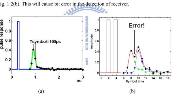
scales at a much lower rate compared to the on-chip bandwidth. The band-limited channel causes intersymbol interference (ISI) and severely degrades the transmitted data. Fig. 1.2 illustrates the phenomenon of ISI. In Fig. 1.2(a), a nice shot pulse gets spread out due to a dispersive channel. When two consecutive pulses are fed into the channel, the output is the summation of the two spread out waveforms, as shown in Fig. 1.2(b). This will cause bit error in the detection of receiver.
(a) (b)
Figure 1.2 Illustration of ISI phenomenon.a (a) An impulse and its response. (b) A series of impulse and their response.
1Reference: “Serial ATA II Electrical Specification Revision 1.0, 26 May 2004.”, ”PCI Express
Base Specification Revision 2.0, 27 Feb. 2009.”, “Universal Serial Bus 3.0 Specification Revision 1.0, 12 Nov. 2008.”, “IEEE Std. 802.3ae: IEEE standard for 10 Gbps Ethernet.”
aThis figure is imaged from the tutorial “Lecture #4 Communication Techniques: Equalization &
Modulation in Advanced Topics in Circuit Design: High-Speed Electrical Interface,” 2004 by Jared Zerbe.
Chapter 1 Introduction
1.2 Motivation and Challenge of High-Speed
Equalizer
The task of equalization is to recover the transmitted data from distortion due to the effect of ISI. As the data rate increases up to multi-Gbps, the impact of ISI on the signal becomes very severe, imposing difficulty on the design of equalizer. To compensate for the signal loss, some approaches have been proposed in high-speed serial links. Pre-emphasis in the transmitter [1]-[4], equalizers in the receiver [5]-[8], or a combination of the two [9]-[12], are employed to do equalization for high data rates. Since the characteristics of channel are not known in advance and they may vary due to variations in environment, adaptive equalizers are preferred in applications for long-time using. Decision-feedback equalizer (DFE) with coefficients adaptation (ADFE) in the receiver has better performance to cancel ISI than adaptive linear equalizer. However, for high data rate application, its design challenge is very high due to signal feedback loops in data path and coefficients updating loops.
In this thesis, the proposed 2-tap adaptive decision-feedback equalizer can cancel post-cursor ISI at data rate of 10 Gb/s. We employ a hopping coefficient update scheme to reduce power consumption and a mixed-signal integrator to save area and enhance the performance. The proposed equalizer is designed in 65-nm CMOS technology.
1.3 Thesis Organization
This thesis is organized as follows:
Chapter 1 Introduction general description of the transmitter, receiver and the role of equalizer in this system is carried out. Then, fundamental concepts of transmission are reviewed, including eye diagram, bit error rate, and so on. Finally, channel modeling will be described.
In chapter 3, we discuss the concept of equalization. Two kinds of equalizers, continuous-time equalizer and discrete-time equalizer, depending on the domain of signal processing will be introduced. Then, a brief derivation of the sign-sign LMS algorithm will be given.
Chapter 4 begins with the overall architecture of our proposed equalizer. We will discuss the key components used in the proposed system. Then, an updating scheme called hopping and the operation of a mixed-signal integrator will be presented. Finally, behavioral simulations of our equalizer on different conditions will be shown. In chapter 5, the implementation of our proposed equalizer will be presented. We will begin with the operation of our equalizer system. Next, circuit design details, simulation results and chip layout are given. Finally, measurement setup consideration is also discussed.
Chapter 2 Overview of Equalizer for Serial Link System
Chapter 2
Overview of Equalizer for Serial
Link System
High-speed serial links have become an indispensable interface in the applications of inter-chip communication. In this chapter, we will give a short overview of serial link system. Next, some basic concepts about signal processing will be given. Finally, we will describe the method of channel modeling.
2.1 Overview of Serial Link System
Fig. 1.1 is a typical block diagram of serial link. The serial link comprises three primary components: a transmitter, a channel and a receiver. The transmitter converts digital bits into a signal stream that is propagated on the channel to the receiver. The receiver transfers this analog signal into binary data. Fig. 2.1 illustrates the signaling in a serial link.
Chapter 2 Overview of Equalizer for Serial Link System A transmitter sends the data as analog symbols. The analog value represents a single bit, known as non-return-to-zero (NRZ). For electrical systems, different levels have different voltages. The duration of each ONE or ZERO is the bit time. The difficulty in a transmitter design is to maintain clean signal levels while transmitting data in high data rates.
In electrical systems, differential signaling is often used. It is a method of transmitting information electrically by means of two complementary signals sent on two separate wires. An important advantage of differential signaling over single-ended signaling is higher immunity to environmental noise. Since the impacts of common-mode noise on differential signals are opposite, the common-mode noise will be rejected by using differential signaling.
The channel is the medium where the data is propagated. This medium would be an optical fiber, a coaxial transmission line, a printed-circuit board (PCB) trace or the chip package. The medium can attenuate or filter the signal and introduce noise.
To recover the bits from the signal, the analog waveform is sampled and equalized. The receiver-end must be able to resolve small inputs at high data rates to recover high-speed signals. An additional circuit, the timing-recovery circuit, properly places the sampling strobe for the receiver to amplify and sample the waveform correctly.
Fig. 2.2 shows a typical serial link with equalizers. The equalizer in the transmitter side can be called pre-emphasis. The topology of this pre-emphasis is usually a feed-forward equalizer (FFE). For a channel that changes with time, the pre-emphasis circuit would need updated information from the receiver. The equalizer set at the receiver side is usually a decision-feedback equalizer (DFE). Since the characteristics of channel may vary due to environment, the coefficients of DFE need to update adaptively. This type of DFE is called adaptive DFE (ADFE). When FFE
Chapter 2 Overview of Equalizer for Serial Link System and DFE are used together optimally, the strengths of both can be cooperated to bear on the channel and maximum performance is obtained.
Figure 2.2 Typical serial link with equalizers.
Fig. 2.3 shows the equalizer in the receiver side. There are two FIR filters in Fig. 2.3: feed-forward filter (FFF) and feed-back filter (FBF). FFF is designed to ease the pre-cursor ISI, and FBF is designed to cancel the remained post-cursor ISI. Many literatures call Fig. 2.3 as a DFE. In this thesis, we define DFE as the dashed area in Fig. 2.3 and define FFF as FFE. We will discuss FFE and DFE in Section 3.2.
Figure 2.3 Block diagram of equalizer in receiver side.
2.2 Basic Concepts
2.2.1 NRZ Data
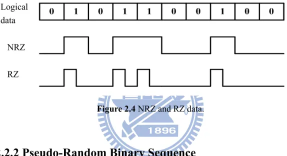
“Non-return to zero” (NRZ) data is a data format used in many high-speed communication systems. As shown in Fig. 2.4, Each logical bit of NRZ data specifies
Chapter 2 Overview of Equalizer for Serial Link System one of two signal levels. This type of waveform is called NRZ to distinguish it from “return to zero” (RZ) data. Each bit of RZ data consists of two sections: the first section represents the bit value, and the second section is always equal to a logical zero. In other words, every two bits are separated by a redundant zero symbol. Because the property of RZ data, it needs about twice as much bandwidth as NRZ data does. This is the reason why NRZ data is much suitable for high-speed applications.
Figure 2.4 NRZ and RZ data.
2.2.2 Pseudo-Random Binary Sequence
Most wire-line communication systems employ binary amplitude modulation. A random binary sequence (RBS) comprises logical ONEs and ZEROs that usually occur with equal probabilities. In Fig. 2.5, if each bit period is Tb seconds, then the bit
rate, Rb, is equal to 1/Tb bits per second. Fig. 2.5 also reveals that the ONEs and
ZEROs assume equal and opposite values, thereby yielding a zero average.
Figure 2.5 Random binary sequence.
Logical data
NRZ RZ
Chapter 2 Overview of Equalizer for Serial Link System In simulation and chip measurement, it is difficult to generate absolutely RBS. Hence it is common to utilize “pseudo-random” binary sequence (PRBS). Each PRBS is a repetition of a pattern, containing a RBS of a number of bits (Fig. 2.6).
Figure 2.6 Pseudo-random binary sequence.
A PRBS of length 2m-1 means the pattern repeats every 2m-1 bits, where m is a positive integer. For example, if there is a PRBS of length 23-1, the sequence will repeat every 7 bits, and the maximum run length is 3. Maximum run length is the maximum number of consecutive ONEs or ZEROs in a pattern. The random nature of data implies that a binary sequence may contain arbitrarily long maximum run length. The long runs produce difficulties in the design of receiver circuits. For instance, in CDR design, the low data transitions during a long run may cause the oscillator to drift and hence generate jitter. Therefore, random data may be encoded to limit the maximum run length. 8-bit/10-bit (8B/10B) coding [13] is a coding algorithm that converts a sequence of 8 bits to a 10-bit word to guarantee a maximum run length of 5 bits. Although the data rate increases by 25%, many aspects of transceiver design can be relaxed.
2.2.3 Intersymbol Interference
Intersymbol Interference (ISI) has been a serious limitation on data rates that can be sent through a communication channel. ISI generally refers to the interference that occurs between the current received bit and other previously received bits. The
Chapter 2 Overview of Equalizer for Serial Link System interference indicates that the portions of previously received bits add to the bit that is being received. This phenomenon can be seen by the following example.
(a) (b)
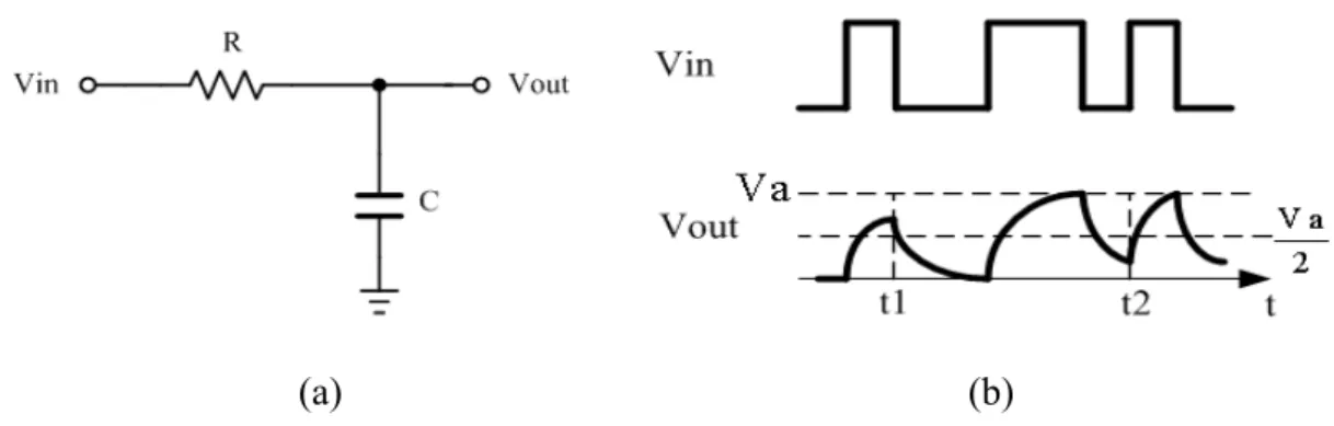
Figure 2.7 (a) A low-pass filter. (b) Effect of low-pass filtering on random data.
Fig. 2.7(a) is a RC low-pass filter, when a random binary sequence passes through it, the high-frequency components are attenuated, as illustrated in Fig. 2.7(b). For a single ONE followed by a ZERO, the output does not reach the peak, but for two consecutive ONEs, it does. The output voltage levels corresponding to ONEs and ZEROs vary with time, making it difficult to define a decision threshold voltage. For example, if the threshold is set at Va/2, the voltages at t=t1, and t=t2 are very
susceptible to noise and the decision circuit may make a wrong decision of bit. Such undesirable phenomenon is called “intersymbol interference” (ISI). ISI produces degradation in system performance and is the major source of bit errors.
In fact, there are two factors that ISI is occurred by the low-pass nature of communication channel. One is the bandwidth of channel, and the other is the density of transitions in the data stream. For the factor of bandwidth, we can see Fig. 2.7 again. The rising edge of output voltage before t=t1 can be expressed as
-t/R C
V (t)=V (1-e ).
out a (2.1)
Therefore, the larger the RC, i.e. narrower bandwidth, the lower output voltage level can reach. For the factor of the transition density of input pattern, Fig. 2.8 is an example to show the problem.
Chapter 2 Overview of Equalizer for Serial Link System
Figure 2.8 Response of long run passes a moderate limited bandwidth channel.
In Fig. 2.8 assume the bandwidth of channel is moderate limited, when more consecutive ONEs are followed by a single ZERO, the output voltage which is supposed to be a ZERO may be far from logical ZERO. It is obvious that the longer the identical series of ONEs before a ZERO, the worse the effect of ISI on the amplitude of the ZERO bit and vice versa. Since the longer the input stays at constant amplitude, the more the channel charges to the amplitude which will make it more difficult to discharge when the input switches.
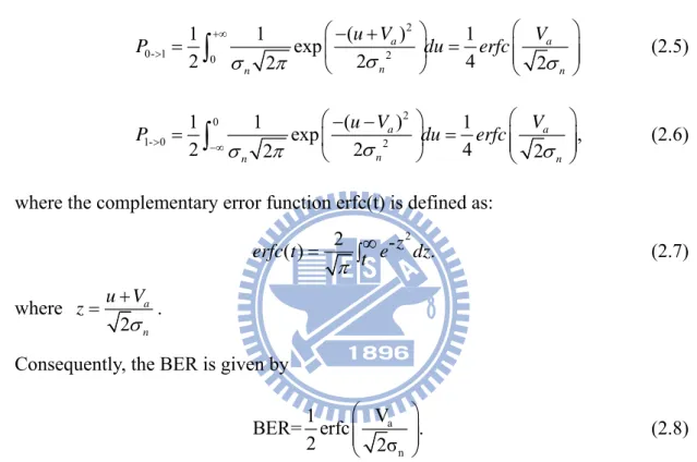
2.2.4 Eye Diagram
As discussed so far, ISI is a function of the bit patterns being sent across the channel. If the input pattern is very long and random, it becomes a very difficult task to find out the effect of ISI on both the amplitude and duration of the received bits. A common method for visualizing the nonidealities in random data is the “eye diagram.” An eye diagram is created by capturing the output waveform which is divided into a short interval, e.g., two bits wide, and overlaid on top of each other. As an example, considering a 2-Gb/s random binary sequence is fed into a first-order low-pass filter having a -3-dB bandwidth of 500 MHz. As depicted in Fig. 2.9, we superimpose all 1-ns intervals to obtain the eye diagram. The two important parameters in an eye diagram are the vertical and horizontal openings of the eye. The vertical eye opening
Chapter 2 Overview of Equalizer for Serial Link System
(a)
(b)
Figure 2.9 An illustration of eye diagram construction. (a) input and output waveform.
(b) eye diagram.
represents the minimum amplitude the received bits can have. On the other hand, the horizontal eye opening defines the time interval over which the data can be sampled without error caused by ISI. In Fig. 2.9(b), we can also observe that the zero crossings experience some deviation from their ideal position. This is called “timing jitter.” As the amount of timing jitter increases, the horizontal eye opening decreases. Therefore, when data rates increase, timing jitter can become a significant problem and cause bit errors in data transmission systems.
Vin
Chapter 2 Overview of Equalizer for Serial Link System
2.2.5 Bit Error Rate
The general definition of “bit error rate (BER)” is BER= number of bit errors .
total number of bits received (2.2)
In other words, the bit error rate (BER) is the percentages of bits that have errors relative to the total number of bits received in a transmission. It is unavoidable that the noise will exist in data transmission. The noise added to the signal degrades both the amplitude and the time resolution, closing the eye and increasing the BER.
Assume the noise amplitude n(t) has a Gaussian distribution with zero mean and a root mean square (rms) value of σn . Thus, we could write the PDF of n(t) as:
2 n 2 n n 1 -n P = exp . 2σ σ 2π ⎛ ⎞ ⎜ ⎟ ⎝ ⎠ (2.3)
Next, if ONEs and ZEROs of the input sequence x(t) occur with equal probabilities, the PDF of x(t) contains two impulses at x=-Va and x=+Va (assume the nominal
values of ONEs and ZEROs are +Va and -Va, respectively), and each has a weight
of 1/2. Having PDF of x(t) and n(t), we could obtain the amplitude distribution of x(t)+n(t), as shown in Fig. 2.10.
As illustrated in Fig. 2.10, x(t)+n(t) shows a PDF consisting of two Gaussian distributions centered around +Va and -Va. The shaded area represents the error
Chapter 2 Overview of Equalizer for Serial Link System samples and the BER can be expressed as:
0 1 1 0
BER=(P−> +P−> ), (2.4)
where P0->1 and P1->0 represent the probability of “receiving a ONE while actually a ZERO is transmitted” and “receiving a ZERO while actually a ONE is transmitted”, respectively.
The probabilities of P0->1 and P1->0 can be derived as [14]:
2 0- 1 0 2 ( ) 1 1 1 exp 2 2 2 4 2 a a n n n u V V P du erfc σ σ π σ +∞ > ⎛ ⎞ ⎛− + ⎞ = ⎜ ⎟ = ⎜⎜ ⎟⎟ ⎝ ⎠ ⎝ ⎠
∫
(2.5) 2 0 1- 0 2 ( ) 1 1 1 exp , 2 2 2 4 2 a a n n n u V V P du erfc σ σ π σ > −∞ ⎛ ⎞ ⎛− − ⎞ = ⎜ ⎟ = ⎜⎜ ⎟⎟ ⎝ ⎠ ⎝ ⎠∫
(2.6)where the complementary error function erfc(t) is defined as:
2 2 -( ) z . erfc t t e dz π ∞ = ∫ (2.7) where 2 a n u V z σ + = .
Consequently, the BER is given by
a n V 1 BER= erfc . 2 2σ ⎛ ⎞ ⎜ ⎟ ⎜ ⎟ ⎝ ⎠ (2.8)
Table 2.1 is the different BERs for different confidence intervals of root mean square value σn. For serial data transmission schemes, the required BER performance
is generally less than about 10-12, which according to this table translates to a necessary minimum margin of over ± 7σn.
In equalizer design, the timing jitter will affect the BER. The causes of jitter can be categorized into two types: deterministic jitter and random jitter. Deterministic jitter is often called a systematic jitter since it is generated by the system. Clock timing jitter and data signal jitter are deterministic jitter and they are predictable and bounded. We usually use peak-to-peak value to measure deterministic jitter. Random
Chapter 2 Overview of Equalizer for Serial Link System jitter, also called Gaussian jitter, is an unpredictable electronic timing noise such as thermal noise. Root-mean-square value is often used to measure the random jitter. Hence, if the random jitter is severe, the value of σn is large, and the BER is large
according to EQ. 2.8.
Table 2.1 BERs for different confidence intervals. interval BER ± 1σn ± 2σn ± 3σn ± 4σn ± 5σn ± 6σn ± 7σn ± 8σn ± 9σn 0.159 2.28 × 10⁻² 1.35 × 10⁻³ 1.84 × 10⁻⁵ 2.14 × 10⁻⁷ 9.87 × 10⁻¹⁰ 1.28 × 10⁻¹² 6.22 × 10⁻¹⁶ 1.13 × 10⁻¹⁹
2.3 Channel Model
In previous sections, we have roughly introduced the effect of ISI on the quality of signal in data transmission. Since ISI arises from some imperfections of channels, in this section, we will discuss the characteristics of channel and build the channel model for our equalizer circuit design.
There are several types of channels utilized in high-speed interconnects, primarily based on the target application. These channels can be roughly classified into three categories. First, for chip-to-chip communication on a printed circuit board (PCB), short copper traces are used. Second, for systems such as local-area network requiring high-speed connection between two computers, coaxial cable or optical
Chapter 2 Overview of Equalizer for Serial Link System fiber is used as the transmission medium. Finally, copper traces along with backplane connectors are employed for high-speed board-to-board communication systems such as routers. In this section, we focus on the PCB traces used for chip-to-chip communication.
The channel is the entire path from the output of the transmitter circuit to the input of the receiver circuit. This includes the connections from the chip I/O pads to the package pin on both sides and the PCB trace that connects them. The termination resistor is used to match the characteristic impedance of the channel for minimizing the signal reflection. As we know, a signal can continue to propagate along a transmission line as long as the impedance remains constant. Changes in the impedance along the line will cause part of the signal energy be reflected which then propagates in the opposite direction. If the signal is reflected again, the second reflection would interfere with the signal that is now transmitted. Hence, it appears as a signal-dependent noise [15].
The source of these reflections occurs at the two ends of transmission line if the energy being propagated is not dissipated. Using a line-termination resistor whose value matches the impedance of the line is the most common solution. Then the voltage and current would follow the Ohm’s law, and reflection will be eliminated. The resistance of the line-termination resistor is usually 50Ω or 100Ω. Error in matching the termination resistor can still cause reflection. The reflection coefficient can be calculated by [16]: L 0 L 0 Z -Z Γ= Z +Z (2.9)
where Γ is the reflection coefficient; ZL is the load impedance; and Z0 is the channel
characteristic impedance.
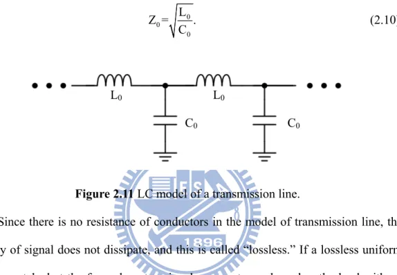
Chapter 2 Overview of Equalizer for Serial Link System interconnect whose length is a significant fraction of the wavelength of interest. An ideal transmission line can be modeled as shown in Fig. 2.11. As depicted in Fig. 2.11, a distributed LC ladder forms the ideal transmission line model. L0 and C0 denote the
inductance and capacitance of the line per unit length, respectively. The characteristic impedance of the line is equal to
0 0 0 L Z = . C (2.10)
Figure 2.11 LC model of a transmission line.
Since there is no resistance of conductors in the model of transmission line, the energy of signal does not dissipate, and this is called “lossless.” If a lossless uniform line is matched at the far end, a step signal propagates and reaches the load with no distortion or attenuation while only exhibiting a frequency-independent delay. A lossless transmission line possesses an infinite bandwidth and a linear phase shift. Unfortunately, there is no this kind of material in practical applications. Essentially, channels must suffer from substantial resistance, and the resulting loss must be taken into account.
The circuit for this signaling medium should be modeled as distributed energy-storage elements, inductance and capacitance, and with some loss due to the series resistor and conductive component of the dielectric. A series of lumped RLGC elements form the lossy channel model, as shown in Fig. 2.12.
L0 L0
Chapter 2 Overview of Equalizer for Serial Link System
Figure 2.12 Lumped RLGC model of transmission line.
In Fig. 2.12, the RLGC is per-unit-length. In high-speed chip-to-chip design, the frequency-dependent attenuation of channel must be taken into account for a reliable communication. Actually, the dominant sources of loss in channels are due to skin effect and dielectric loss. At high frequencies, current flows closer to the surface of the conductor, reducing the area of current flow and increasing the resistive loss. This is known as skin effect. Since the dielectric material for PCB is not a perfect insulator, it leads to a DC loss associated with the resistive drop between the signal conductor and reference plane. If the frequency of signal increases, the dielectric loss would be worsened. Here, the resistor R embodies both low-frequency and high-frequency conductor losses while conductor G models the dielectric loss. The characteristic impedance of the lumped RLGC model is equal to [17]:
0
R+jwL
Z = .
G+jwC (2.11)
When the frequency of signal increases, the current propagates closer to the surface of the conductor with a limited depth. This is called skin depth (δ) and it can be expressed as [18]:
1
δ = ,
π f μ σ⋅ ⋅ ⋅ (2.12)
where f is the frequency, μ is the permeability (4π × 10-9 H/m for copper), and σ is the conductivity of the conductor. If the frequency (fS) is above the point where δ is half
Chapter 2 Overview of Equalizer for Serial Link System must be considered. Here fS is given by
S 2 1 f = . t ( ) π×μ×σ 2 (2.13)
Above this frequency, the resistance of the conductor can be calculated as
DC S
f R(f) = R .
f (2.14)
An equation for the loss due to skin effect for a transmission line of length L is given by 0 ( ) 2 DC S S R f A f Z f = (2.15)
Moreover, the attenuation due to dielectric loss is given by
tan ( ) r D , D f A f c π ε ⋅ ⋅ δ = (2.16)
where εr is the relative dielectric constant of the dielectric, tan δD is the loss tangent of
the dielectric, and c is the speed of light [18]. The loss due to skin effect is proportional to the square root of f and typically dominates the total loss at low frequencies. On the other hand, dielectric loss is proportional to f, and therefore, determines the total loss at high frequencies.
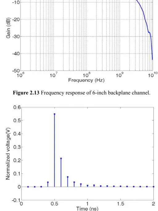
Fig. 2.13 and Fig. 2.14 shows the frequency and impulse responses of 6-inch backplane channel model by using MATLAB, respectively. Note that this model is from practical measurement of backplane channel. We can observe that when frequency is at 5GHz, the attenuation is about 15dB. Fig. 2.14 reveals the impact of ISI. The highest tone is the main cursor. The right-hand side of main cursor is called post-cursor ISI and the left-hand side of main cursor is called pre-cursor ISI. We will discuss the pre- and post-cursor ISI in Sub-section 3.2.1. We can observe that the first and second post-cursor ISI dominate the overall ISI and this information gives us a
Chapter 2 Overview of Equalizer for Serial Link System
Figure 2.13 Frequency response of 6-inch backplane channel.
Figure 2.14 Impulse response of 6-inch backplane channel. guideline to design our equalizer.
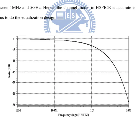
Although having the channel model in MATLAB, we still have to create the model for HSPICE. With the help of the built-in field solver in HSPICE, a set of RLGC elements can be calculated according to the frequency response and the material properties. The channel model in HSPICE is called a W-element transmission line. HSPICE models the skin effect resistance of the conductor and the dielectric
Chapter 2 Overview of Equalizer for Serial Link System conductance of the insulator using the following equations [19],
R(f) = R +R0 S⋅ f , (2.17)
G(f)=G +G0 D⋅f . (2.18) where R0 is the DC resistance in O/m, Rs is the skin effect parameter in O/m Hz, G0
is the DC conductance of the dielectric in S/m, and GD is the dielectric loss parameter
in S/m Hz⋅ .
Fig. 2.15 shows the frequency response of channel model in HSPICE. Because the channel model created in HSPICE needs to fit the model in MATLAB, we have to compare the difference between both. Fig. 2.16 illustrates errors in frequency response between the two models. Obviously, it shows the accuracy is within ± 1dB between 1MHz and 5GHz. Hence, the channel model in HSPICE is accurate enough for us to do the equalization design.
Chapter 2 Overview of Equalizer for Serial Link System
Chapter 3 Equalization Basis
Chapter 3
Equalization Basis
Equalization is a kind of signal processing. The equalizer deals with the data received from the channel output and then transfers the equalized data to the circuit after it. Equalization method can be categorized into two types depending on the domain of signal processing: a continuous-time equalizer and a discrete-time equalizer. In Section 3.1 and 3.2, we will give a brief introduction of these two categories and focus on the decision-feedback equalizer. In Section 3.3, we will introduce an adaptive algorithm: sign-sign LMS algorithm. This algorithm will play an important role in the design of our equalizer system.
3.1 Continuous-Time Equalization
The continuous-time equalizers do equalization without the timing information. The signal processed by continuous-time equalizer is not digitized. They always do equalization in the frequency domain. Since the characteristic of channel is usually a low-pass filter type, continuous-time equalizers are like high-pass filters to compensate or to equalize the frequency response of the channel. Hence, we can view the continuous-time equalizer as a high-pass filter. This equalizer has a trend of increasing gain in high frequency to compensate the gain loss of the channel. Using continuous-time equalizer between the channel and receiver, we expect the high pass response can just compensate the loss of channel at high frequency to flat or to
Chapter 3 Equalization Basis equalize the total effective response. If we can not equalize the response, at least we can make frequency band nearly flat. Fig. 3.1 roughly illustrates the goal of this kind of equalizer.
Figure 3.1 Channel response and equalizer response.
However, any circuit has its poles and zeros. That means to reach infinite high gain at the infinite high frequency is impossible. Gain amount of frequency response will fall after an limited frequency range. Fig. 3.2 illustrates the practical frequency response of continuous-time equalizers. In this figure, we use piece-wise to sketch a roughly Bode plot. We assume there is a zero at a relative low frequency in the equalizer circuit. The response will increase in 20 dB/dec when there is a zero. The
Chapter 3 Equalization Basis gain keeps rising with the frequency increasing until reaching the first pole. The first pole cancels the rising frequency of the zero and flats the frequency response. As the frequency keeps increasing, the gain will drop dramatically due to the dominant pole introduced by the circuit itself.
Obviously, in order to compensate the loss of channel, continuous-time equalizers create the zero to produce a gain pulse in high frequency part. Allocating the first zero and first pole at proper frequency, we can move the gain pulse to the band we focus on. Although the effective response is not flat through the whole frequency, the equalizer extends the flat part toward the range of data transmission frequency.
A continuous-time equalizer is truly a simple one tap continuous-time circuit with high-frequency gain boosting transfer function that effectively flattens the channel response. The equalizer can be implemented by passive components or active components. As an example, the required frequency shaping can be achieved by a simple RC network as shown in Fig. 3.3. The resistor attenuates the low-frequency signals while the capacitor allows the high-frequency signal content, thus resulting in high frequency gain boosting. The transfer function and the pole zero frequencies are given by:
Chapter 3 Equalization Basis 2 1 1 1 2 1 2 1 2 1 2 1 ( ) 1 ( ) R sR C H s R R R R C C s R R + = + + + + (3.1) 1 1 1 z w R C = (3.2) 1 2 1 2 1 2 1 ( ) p w R R C C R R = + + (3.3)
The gain-boost factor is proportional to the ratio of zero and pole frequency ωp/ωz, so reasonable amounts of equalization can be achieved by choosing appropriate
component values that set the required gain-boosting. There are two main drawbacks with simple passive RC equalizers. First, the RC network introduces large impedance discontinuity at the channel and equalizer. Employing inductors for impedance matching networks can be used to prevent the discontinuity. However, the large inductors make this approach less suitable for on-chip integration. Second, this method can not improve SNR since equalization is performed by attenuating low-frequency signal spectrum. Due to these reasons, this technique has limited use in high-speed serial links.
It is desirable to have a gain greater than one at all frequencies to maximize the benefit from receiver-side equalization. Therefore, equalizers using active circuit elements rather than passive components are required to achieve gains greater than one. Since parallel RC combination introduces a zero in the transfer function, it is possible to degenerate the transistors in a differential pair such that their effective transconductance increases at high frequencies [6][7][20]. Shown in Fig. 3.4, such an arrangement employs both capacitive and resistive degeneration. We express the equivalent transconductance as ( 1) 1 1 / 2 1 ( || ) 2 2 m m S S m S S S m S m S g g R C s G R R C s g R g C s + = = + + + (3.4)
Chapter 3 Equalization Basis
Figure 3.4 Continuous-time equalizer using capacitive degeneration. where gm is the MOS (M1,M2) tranconductance.
Hence, 1 z S S w R C = (3.5) 1 1 m S / 2 p S S g R w R C + = (3.6) 2 1 p L L w R C = (3.7) _ 1 / 2 m L m S g R DC gain g R = + (3.8) By designing the zero frequency to be lower than the dominant pole, considerable high frequency gain boosting can be achieved and it will looks like the frequency response in Fig. 3.2. However, the maximum gain boosting achieved by this method is limited by the bandwidth of the amplifier due to the load capacitance. There are several other broadband techniques for equalizing filters proposed, like inductive peaking [20], Cherry Hopper amplifier [7], or combination of inductive peaking and Cherry Hopper amplifier [21]. The goal of these circuits is to widely extend the effective gain boosting in higher frequencies.
Chapter 3 Equalization Basis sampling clock to perform equalization, continuous-time equalizers just provide high-frequency boost to equalize the band. However, the gain-peaking transfer function of the equalizer amplifies the high frequency noise that degrades the noise margin. Moreover, the adaptation mechanism of continuous-time equalizers is more complex than that of discrete-time ones. These are disadvantages of continuous-time equalizers.
3.2 Discrete-Time Equalization
Discrete-time signal processing is for signals that are defined only at discrete points in time. The processing contains the concept of timing index and the order of data becomes a key parameter in operation. Discrete-time equalizer has the same idea of equalizing signals in discrete data points. However, the essential meaning of the discrete-time equalizers is to cancel the intersymbol-interference (ISI) induced by imperfect characteristics of channels at the discrete data points. The discrete-time equalizers can be categorized into two depending on canceling different parts of ISI: a feed-forward equalizer and a decision-feedback equalizer. We will discuss these two kinds of discrete-time equalizers in the followings.
3.2.1 Pre-and Post-Cursor ISI
Before introducing discrete-time equalizers, we investigate ISI again but this time we will look ISI in different point of view. We have known ISI can be thought of as the effect of past and future symbols on the current symbols. Assume that the impulse response of channel is h(t) and the transmitted signal is x(t), and the signal in
Chapter 3 Equalization Basis the channel output, y(t), is the convolution of x(t) and h(t), y(t)=x(t)*h(t). Hence, the data received at timing index n can be expressed as
0 ˆ [ ] [ ] [ ] [ ] [ ] [ ] [ ] [ ] m m y n x n h n x m h n m x n h n ISI y n ISI ∞ =−∞ ≠ = +
∑
− = + = + (3.9)We can write y[n] in another form:
2 1 0 1 2 ˆ ˆ ˆ ˆ [ ] [ ] ... [ 2] [ 1] [ ] ˆ ˆ ˆ [ 1] [ 2] ... [ ] m k y n c y n m c y n c y n c y n c y n c y n c y n k − − − = + + + + + + + + − + − + − (3.10)
The equation shows the current symbol y[n] (with some factor c0) along with
some factor (cm…ck) of k past symbols and m future symbols respectively. The
roll-off of the rising edge of a pulse can be treated to have an effect on the next bit (bit on the left in a pulse train) and is called pre-cursor ISI. The roll-off of the falling edge of the pulse can be treated to have an effect on the previous bit (bit to right in pulse train) and is called post-cursor ISI. Fig. 3.5 illustrates a discrete-time representation of an impulse response with pre- and post-cursor ISI. In a practical system, it is reasonable to assume that the ISI affects a finite number of symbols. Hence we can assume cn=0 for n<-m and n>k, where m and k are finite, positive integers.
Chapter 3 Equalization Basis
3.2.2 Feed-Forward Equalizer
The simplest discrete-time equalization technique that has been used over the years is linear feed-forward equalization. Feed-forward equalization typically involves the use of a linear transversal finite impulse response (FIR) filter as shown in Fig. 3.6. Here we use a 3-tap FFE as an example. The FIR filter consists of adjustable tap coefficients, C-1, C0, C1, with a time delay, D between adjacent taps. The output of
the FFE is a summation of the input signal with delayed versions of itself. Depending on the relative values of C-1, C0, and C1, the FFE can be used to cancel pre- and
post-cursor ISI, only pre-cursor ISI, or only post-cursor ISI. The tap coefficients C-1,
C0, and C1 are calculated using algorithms designed to meet certain system criteria.
We can write the equation of output ˆy of the FFE as: D
1 0 1
ˆ [ ]D [ ] [ 1] [ 2]
y n =C y n− +C y n− +C y n− (3.11)
where y[n] is the output signal of channel. Since y[n] can be expressed as x[n]*h[n], where x[n] is the transmitted signal and h[n] is the impulse response of channel, EQ. 3.11 can be re-written as:
Chapter 3 Equalization Basis 1 2 1 0 1 ˆ ( )D ( ) ( )( ) Y z = X z H z C− +C z− +C z− (3.12) Since 1 2 1 0 1
C− +C z− +C z− is the z transform response of equalizer, we write it as
E(z). Hence, if the output ˆ [ ]y n is perfectly equal to input x[n], e.g. there is no D
error occurred, the equation about equalizer and channel responses is ( ) 1
( )
E z
H z
= (3.13) EQ. (3.13) is an illustration of zero-forcing (ZF) equalization. ZF equalization tries to cancel all the ISI and results in a transfer function that is the exact inverse of the channel response. While this might sounds like an ideal solution, ZF equalization implies gain in the frequency range where the channel response is small. Because channels are usually low-pass filters in nature, this type of equalizers will be high-pass response. Any additive noise in that frequency range is also amplified. So in noisy channels, the ZF-FFE can result in very poor SNR at the output.
In fact, Fig. 3.6 is an analog FIR equalizer. An analog delay chain is required to implement the analog FIR. This analog delay can be implemented using a replica delay line whose delay is locked to a delay locked loop or a phase locked loop operating at data rate [8]. However, there are some difficulties occurred in the FIR analog equalizer. First, the settling time of the front-end sample-and-hold (SHA) limits the overall operating speed. Second, the sampled signal experiences attenuation due to the limited bandwidth of the delay elements. Finally at high data rates, the precise generation of analog delay elements consumes large power. One alternative way to generate the analog delay is by using multi-phase (φ φ1 ~ n) clocks. By paralleling several data path, the circuit can slow down its operation frequency. The conceptual block diagram of a parallelized architecture is shown in Fig. 3.7.
Chapter 3 Equalization Basis
Figure 3.7 A parallelized analog FIR equalizer.
FFE has been shown to be effective on channels where the ISI is not severe. As mentioned earlier, the FFE amplifies noise on channels, resulting in poor SNR. Therefore, non-linear equalizers such as the decision-feedback equalizer (DFE) have been explored and we will discuss it in the next sub-section.
3.2.3 Decision-Feedback Equalizer
Decision-feedback equalization [22] is a non-linear equalization that employs previous decisions to eliminate the ISI caused by previous symbols on the current symbol. It was first introduced by M. E. Austin in 1967, who introduced a decision-theory approach to solve the problem of digital communication over known dispersive channels. This work was the first to describe a method to utilize the information of past decisions to make corrections to current symbols and thereby cancel post-cursor ISI. Today the DFE is used extensively to combat ISI in different dispersive channels and finds many applications in high-speed communication systems.
A typical decision-feedback equalizer is shown in Fig. 3.8. Here we use one tap of DFE as an example. The signal,ˆy , is the summation of received data and the D previous decision bit multiplied by a constant C1. The slicer is a decision-making
Chapter 3 Equalization Basis
Figure 3.8 Typical block diagram of DFE with one tap. ≧Vref, the output of slicer is ONE and it is ZERO when yD < Vref.
Now we will explain why the DFE can cancel the post-cursor ISI. We can write the transfer function for the simple one-tap DFE as
1
ˆD[ ] [ ] sgn( [ˆD 1])
y n = y n +C y n− (3.14)
where y[n] is the signal level being received, ˆ [ ]y nD is the DFE corrected signal, C1 is
the first DFE feedback tap weight, and sgn() produces a 1 for ˆ [y nD − ≧ 0 and -1 1] otherwise. For the case of zero-error detection, EQ. (3.14) can be analyzed in a linear sense by replacing sgn ( ˆ [y nD − ) with the transmitted data x[n-1] and y[n] with the 1] convolution of sequence x[n] with the channel response h[n]. The resulting difference equation and corresponding z transform are
1 1 1 ˆ [ ] ( [ ]* [ ]) [ 1] ˆ ( ) ( )( ( ) ) D D y n x n h n C x n Y z X z H z C z− = + − = + (3.15)
To illustrate the operation of the DFE, assume a low-pass channel-response function
1
( ) [0] [1]
H z =h +h z− (3.16)
with h[0] normalized to 1 and h[1] positive, resulting in reduced gain at high frequencies. In this case
1 1 1
ˆ ( )D ( )(1 [1] )
Y z =X z +h z− +C z− (3.17)
Chapter 3 Equalization Basis equalized channel Yˆ ( )D z =X z( ).
The biggest bottleneck of the simple DFE is its operation speed. Before the next bit comes, the feedback signal must be ready at the input of adder. This implies that the total propagation delay consumed by the slicer, the flip-flop, multiplier, setup time of flip-flop and some operating margin, needs to be less than one symbol period. This loop is a critical path in the DFE. As data rate increases to several multi-Gbps, it seems that the critical path delay can not meet the stringent timing constraint. For example, if the data rate is 10 Gb/s, the total latency of the critical path must be less than 100 ps. Unless the propagation delay of silicon processing elements improves greatly and overcomes this difficulty, high data rates will limit the use of this direct type of DFE.
In order to overcome the feedback loop latency challenge imposed by the limitations of the clocked topology, designers have come up with some novel design techniques to implement multi-Gbps DFEs in standard CMOS. A common approach to reduce the critical path delay is to use a “look-ahead” architecture, also referred to as loop-unrolled DFE or speculative DFE [23]. The architecture is shown in Fig. 3.9. The basic concept behind this technique is that for a NRZ signal, every symbol is a 1 or a -1. The two threshold value V1 and V0 are the first tap weight, C1, multiplied by 1
and -1, respectively. Instead of feeding back the slicer decision for the first tap, a look-ahead DFE makes two decisions with two slicers where each slicer assumes the previous bit is a -1 and 1. The received data value is selected from these two slicer outputs based on the previous data value with a multiplexer. The nthdecision yD can
be expressed as
1 0
[ ] [ ] [ 1] [ ] [ 1]
D D D D D
y n = y n y n− +y n y n− (3.18)
Chapter 3 Equalization Basis
Figure 3.9 Look-ahead one-tap DFE.
1 0
[ 1] [ 1] [ 2] [ 1] [ 2]
D D D D D
y n− = y n− y n− +y n− y n− (3.19)
Substituting EQ. (3.19) in EQ. (3.18), an can be expressed as
(
)
(
)
(
)
(
)
1 1 0 0 1 0 1 1 0 1 1 0 0 0 1 [ ] [ ] [ 1] [ 2] [ 1] [ 2] [ ] [ 1] [ 2] [ 1] [ 2] [ ] [ 1] [ ] [ 1] [ 2] [ ] [ 1] [ ] [ 1] [ 2] [ D D D D D D D D D D D D D D D D D D D D D y n y n y n y n y n y n y n y n y n y n y n y n y n y n y n y n y n y n y n y n y n f = − − + − − + − − + − − = − + − − + − + − − = n y n] [D − +2] f n y n2[ ] [D −2] (3.20)EQ. 3.20 shows that yD[n] is now a function of yD[n-2] and not yD[n-1]. This
implies that the critical timing path has been extended from Tbit to 2Tbit, where Tbit is
one bit period. The extra delay available can be used to reduce the clock rate to half the data rate. The half-rate architecture of look-ahead DFE is shown in Fig. 3.10. Obviously, this approach has the advantage of lower clock rate but the hardware and area increase tremendously.
The look-ahead technique is typically limited to only one tap because of an exponential increase in the number of slicers with the number of taps. As a result, the second and higher order taps of the DFE do not apply look-ahead and are often fed back directly. We call this dynamic feedback technique [9][10]. A lot of creative
Chapter 3 Equalization Basis
Figure 3.10 Half-rate look-ahead DFE.
inventions about dealing the timing constraint, higher data rates and lower power consumption, have been proposed [24][25].
The problem of noise enhancement can be completely eliminated by using DFE since the DFE just utilizes the previous decision to do the equalization without boosting the high-frequency noise. There are two design issues with the DFE design. First, the effectiveness of ISI cancellation is based on the assumption that all previous decisions are correct and therefore if decisions are incorrect, the ISI will be worse. The problem is referred to as error propagation. However, in the case of serial-links with required BER < 10-12, error propagation does not degrade the performance. Second, the DFE can cancel only post-cursor ISI. If the channel response is very severe, including pre- and post-cursor ISI, a separate FFE is required.
Chapter 3 Equalization Basis
3.3 Sign-Sign LMS Algorithm
The sign-sign least-mean-square (sign-sign LMS) algorithm is a simplification of least-mean-square (LMS) algorithm [26]. In this section, we will give a short derivation of LMS algorithm and point out the relationship between LMS and sign-sign LMS algorithms. Finally, the concept of adaptive equalizer will be described.
First, we introduce the method of steepest descent. Fig. 3.11 shows a N-tap FIR Wiener filter. In the figure, d[n] is the desired response or the correct output that we expect. We define four parameters as follows:
tap-weight vector: T
0 1 N-1
W=[W W ... W ] , signal input: X[n]= x[n] x[n-1] ... x[n-N+1] ,
[
]
T filter output: y[n]=W X[n], Terror signal: e[n]=d[n]-y[n].
The cost function is defined as the mean-square error
2 2
C T T
F =E e [n] =E d [n] -2W P+W RW⎡⎣ ⎤⎦ ⎡⎣ ⎤⎦
Chapter 3 Equalization Basis where R=E X[ ]X [ ]T
n n
⎡ ⎤
⎣ ⎦ is autocorrelation of the filter input. FC has a single global
minimum obtained by solving the Wiener-Hopf equation RWopt = P
if R and P are available, where Wopt is the optimal tap-weight vector. However, we
can use iterative method rather than solving the Wiener-Hopf equation directly. Starting with an initial guess for Wopt, say W[0], a recursive search method that may
require many iterations to converge to Wopt is used.
The method of steepest-descent is a gradient-based method. Using the initial or present guess, we compute the gradient vector and evaluate the next guess of the tap-weight vector by making a change in the initial guess in a direction opposite to that of the gradient vector. Here, we define the gradient of FC as
C
F =2RW 2P
∇ − (3.21) With an initial guess of W[0] at n=0 the tap-weight vector at the k-th iteration is denoted as W[k]. We can write down the recursive equation that is used to update W[k]:
[ 1] [ ] k C
W k+ =W k − ∇μ F (3.22)
where μ > 0 is called the step-size, ∇kFCdenotes the gradient vector ∇ calculated at k
the point Wopt.=W[k].
If we substitute EQ. (3.21) into EQ. (3.22), we get
[ 1] [ ] 2 ( [ ] )
W k+ =W k − μ RW k −P (3.23)
By EQ. (3.23), W[k] will converge to the optimum solution Wopt and the convergence
speed is dependent on the step-size μ.
The LMS algorithm is a stochastic implementation of the steepest-descent algorithm. It simply replaces the cost function 2[ ]
C
Chapter 3 Equalization Basis estimate ˆ 2[ ]
C
F =e n . By substituting the simplified cost function into EQ. (3.22), we
obtain 2 [ 1] [ ] [ ] W n+ =W n − ∇μ e n (3.24) where 0 1 1 ... T N W W W − ⎡ ∂ ∂ ∂ ⎤ ∇ = ⎢∂ ∂ ∂ ⎥
⎣ ⎦ . We can expand the i-th element of the
gradient vector 2[ ] e n ∇ as 2[ ] [ ] [ ] 2 [ ] 2 [ ] 2 [ ] [ ] i i i e n n y n e n e n e n x n i W W W ∂ = ∂ = − ∂ = − − ∂ ∂ ∂
then, we will get
2[ ] 2 [ ] [ ]
e n e n X n
∇ = − (3.25)
where [ ]
[
[ ] [ 1] ... [ 1]]
TX n = x n x n− x n− +N .
Finally, we can get the LMS algorithm by substituting EQ. (3.25) into EQ. (3.24)
[ 1] [ ] [ ] [ ]
W n+ =W n + ⋅μ e n X n⋅ (3.26)
Here, we merge the constant 2 into the step size μ.
EQ. (3.26) describes the relationship between the new tap weight and the current tap weight of LMS algorithm. The sign-sign LMS algorithm is a simplicity of the LMS algorithm. Using the sign of e(n) and X[n] instead of the actual value of them simplifies the tap weight calculation. The sign-sign LMS algorithm is
(
)
(
)
[ 1] [ ] [ ] [ ]
W n+ =W n + ⋅μ sign e n ⋅sign X n (3.27)
where the sign() is a function that gets the sign of input. Since sign-sign LMS algorithm is a simplicity of the LMS algorithm, there is a shortcoming about sign-sign LMS algorithm. When coefficients converge, the error in sign-sign LMS algorithm will be larger than that in LMS algorithm. However, the values of sign error and data imply that the complexity of circuit design can be largely reduced.
Chapter 3 Equalization Basis known a priori, and they may vary due to the variations of materials or environment. Hence, the equalizer coefficients need to update adaptively. The conceptual block diagram illustrating the operation of an adaptive one-tap DFE is shown in Fig. 3.12 [27]. The coefficient update processor uses an algorithm like LMS or sign-sign LMS to automatically adjust the coefficients by measuring the equalizer performance so as to improve the performance on an average.
Chapter 4 Discrete-Time Adaptive Decision-Feedback Equalizer
Chapter 4
Discrete-Time Adaptive
Decision-Feedback Equalizer
In Chapter 2 and Chapter 3, we have generally introduced the basic concepts, channel model, and the classification of equalizers. In this Chapter, we will demonstrate our proposed architecture of equalizer and explain the behaviors of these blocks. Finally, some behavioral simulation results will be presented.
4.1 DT-ADFE Architecture
Chapter 3 has illustrated the category of receiver equalizers depending on the domain of signal processing: a continuous-time equalizer and a discrete-time equalizer. Since continuous-time equalizers introduce noise enhancement in high frequency band and adaptive method in continuous-time equalizers is difficult to implement, we choose our equalizer type as discrete-time version.
Fig. 4.1 is the block diagram of discrete-time adaptive decision feedback equalizer. We will discuss in details of the proposed architecture. As depicted in Fig. 4.1, the architecture is a typical model of ADFE. Discrete-time ADFE needs a clock to sample the data and make the decision. The clock rate and then the bit rate depends on the feedback latency. If the latency is more than one bit period in a full-rate architecture, it must be considered to lower the clock rate and employ look-ahead architecture and so on. The discrete-time equalizer has benefits in speed as it can