旋塗式有機主動層薄膜電晶體的製程改善與可靠度分析
123
0
0
全文
(2) 旋塗式有機主動層薄膜電晶體的製程改善與可靠度分析. 指導教授: 葉清發、羅正忠 博士. 研究生:林榮祥. 國立交通大學 電子工程學系 電子研究所碩士班. 摘要. 近年來,有機顯示器成為市場上的前瞻技術,利用有機發光二極體和有機薄膜電晶 體已經可以製作出低成本、可彎曲、全彩的平面顯示器。本論文以“bottom contact"的 結 構 , SiO2 為 絕 緣 層 , 利 用 旋 塗 的 方 式 成 長 有 機 薄 膜 , 成 功 地 製 作 出 以 poly(3-hexylthiophene)、簡稱 P3HT 為有機材料的有機薄膜電晶體。 在第二章當中,我們利用二甲苯和氯仿這兩種不同的溶劑來溶解 P3HT,可發現當 P3HT 的重量百分濃度高於 0.3%時,就無法完全溶解於二甲苯中,並留下許多微小顆粒, 而氯仿則能夠溶解高濃度的 P3HT (> 2 wt%),顯示氯仿對於 P3HT 而言是一種極佳的溶 劑。此外,我們發現以氯仿為溶劑所製作出來的有機薄膜電晶體能夠有效地抑制異常的 閘極漏電流,當 P3HT 的重量百分濃度超過 0.8%時,會有明顯的 bulk 漏電流現象產生, 以 0.3%之 P3HT 製成的薄膜電晶體則可以獲得最低的表面粗糙度以及較佳的元件特性。 在第三章當中,有機薄膜電晶體分別經由不同時間的真空處理、氧氣處理、氮氣處 理、泡水處理或閘極偏壓 stress;由於氧氣是 P3HT 的摻雜物之一,經由氧氣處理之有機 薄膜電晶體的臨限電壓值與漏電流會隨著氧氣處理時間而大幅增加,氮氣和真空處理都 可以降低 P3HT 薄膜內的氧含量,故可有效改善元件特性;至於泡水處理則對於有機薄 膜電晶體的特性不會產生明顯的影響。在閘極施加正的偏壓 stress 會使 P3HT 內部的耦 極重新排列,並造成臨限電壓的正偏移,閘極負偏壓 stress 則會使臨限電壓往負方向偏 i.
(3) 移。 在第四章當中,我們利用鉑、金、鎳和鈦來當作有機薄膜電晶體之源極和汲極的電 極材料,由於鉑跟金的功函數大於 P3HT,兩者都能夠和 P3HT 形成較佳的歐姆接觸,以 鎳為源極/汲極電極材料的電晶體,則在低汲極電壓下產生 crowding effect。我們亦改變 附著層金屬和接觸層金屬的厚度比例來觀察其對電性的影響,但是實驗發現接觸電阻受 其影響的程度非常小。. ii.
(4) The Analysis of Process Improvement and Reliability Characteristic of Spin-On Organic TFT. Student: Jung-hsiang Lin. Advisor: Dr. Jen-Chung. Lou Dr. Ching-Fa Yeh Department of Electronics Engineering & Institute of Electronics National Chiao Tung Unversity. Abstract Recently, active matrix organic diode displays (AMOLEDs) become the most advanced technology in the market; organic light-emitting diodes (OLEDs) and organic thin film transistors (OTFTs) enable the fabrication of low-coat, flexible, full color flat panel displays. In this paper, organic thin film transistors based on poly (3-hexylthiophene) (P3HT) with the “bottom contact”structure, SiO2 as insulating layer, organic active layer grown with spin-coating have successfully been demonstrated. In chapter 2, we used two kinds of solvents, xylene and chloroform, to dissolve P3HT. While weight percentage is as high as 0.3%, the P3HT cannot completely be dissolved in xylene and then many clusters of undissolved P3HT powder is observed. However, chloroform can dissolve high weight percentage of P3HT (> 2 wt%). Therefore, it is proved that chloroform is a good solvent for P3HT. Furthermore, we observed that the anomalous gate leakage current was suppressed by fabricating OTFTs with chloroform solution. As the weight percentage of P3HT is above 0.8%, it would cause obvious bulk leakage current. In summary, the P3HT OTFTs fabricated by 0.3% chloroform solution can acquire the lowest surface roughness and the better performance of devices than others. iii.
(5) In chapter 3, the OTFTs are treated with vacuum treatment, O2 treatment, N2 treatment, immersed in water or gate bias stress for different time. Since oxygen is a kind of dopant for P3HT, threshold voltage and leakage current of the OTFTs drastically increase with O2 treatment time. Vacuum and N2 treatments can be used to recover some of the lost performance through vacuum-induced expulsion of absorbed oxygen. As regards the OTFTs being immersed in water, the performance of electrical characteristics would not be affected. When a positive bias was applied to the gate electrode, it would lead to the dipole moment arranging in the P3HT polymer and positive threshold voltage shift. Negative gate bias stress causes negative threshold voltage shift. In chapter 4, we use Pt, Au, Ni or Ti as S/D contact materials of OTFTs. Because the work function of Pt and Au are larger than the work function of P3HT, they can form better ohmic contact with P3HT than others. Nevertheless, it was observed that the crowding effect was occurred at the small drain bias for Ni as S/D contact material of OTFTs. Secondly, we adjusted the thickness ratio of adhesion/contact metals, such as Ti/Pt and Ti/Au. From experiment results, it was observed that contact resistance is weakly dependent on the thickness ratio of adhesion/contact metals.. iv.
(6) 誌. 謝. 葉清發、羅正忠教授: 感謝葉清發老師在我碩士生涯的一開始給予我精神上的支持和鼓勵,讓我重新調 整自己面對問題和解決問題的方法及態度,並且調整自己的求學態度。感謝羅正忠老師 在實驗方面的規劃和指導,才能夠順利的將實驗完成。 我的家人: 感謝我的父親林崑山、我的母親林碧華和我的弟弟林榮泰,因為他們的栽培,我 才能夠在求學的路程上順利的完成我的學業;因為他們的支持和鼓勵,我才能夠突破我 人生中的每一項關卡。 實驗室學長: 感謝實驗室學長陳添富、蕭智文和王碩晟。尤其要感謝王碩晟學長,在我做實驗 沮喪時,給我安慰;在我做實驗茫然時,指引我方向;在我做實驗灰心時,給予我信心。 也感謝陳添富和蕭智文學長在各方面的關心和指導。 實驗室學弟: 感謝實驗室學弟鍾漢邠、蔣陳偉、陳昶維、施俊宏、洪啟哲和吳伯慶。尤其要感 謝鍾漢邠,在我實驗最忙身體又不適的時候,給予最為即時的幫助。也感謝蔣陳偉和陳 昶維接下實驗室管理方面的工作,表現的非常認真和努力。也要感謝施俊宏幫我解決電 腦軟體上的一些問題。 實驗室同學: 感謝實驗室同學劉俊彥和薛國欽。在課業上的切磋及討論,能夠順利渡過每一堂 課。 我的女友: 感謝我的女友賴錦怡,在這一年多來陪我走過碩二最辛苦、最忙碌的時期;也能 體諒我做實驗的忙碌,不能常常陪伴她;也能包容我的許多小疏忽。 大學同學: 感謝我的大學同學莊嘉平、王聖元、宋英超、劉哲宏、余俊德、謝怡慧、蔡仁祥、 宋英超、楊士昌和陳慶勳。由於彼此互相的關心和鼓勵,使在新竹讀書的每個人都能順 利的取得了碩士學位。. v.
(7) 曾信榮學長: 感謝曾信榮學長,在我覺得孤單和無助時,陪我聊天,讓我能夠重新振作起來。 教會的朋友: 感謝教會朋友政忠、世學、哲維、佳垣、皇興以及其他未提到的朋友。因為有你 們的建議和幫忙,在面臨許多選擇的同時,在面對挫折及迷惘時,給予了相當的思考空 間及改變。 最後我要將我的碩士論文獻給我最愛的人-我的母親,希望她能夠在世界的另外一 方看到我的成長。. vi.
(8) Contents Abstract (in Chinese)………………………………………………………………………….i Abstract (in English)……………………………………………………………....................iii Acknowledgement…………………………………………………………………………….v Contents……………………………………………………………………………………...vii Figure Captions………………………………………………….…………………………...x Table Captions…………………………………………………….…………………………xi Chapter 1 Introduction 1.1 General Background and Motivation…………..……………………………………….1 1.2 Charge Transport in Organic Semiconductor….…………………………...………….2 1.3 Operation of Organic Thin Film Transistors…………………………………………...3 1.4 Thesis Organization………………………………………………………………………4 Chapter 2 Property of P3HT and Spin-Coating technique 2.1 Introduction……………………………………………………………………………...11 2.2 The Molecular Structure of P3HT……………………………………………………..12 2.3 Fabrication of Organic Thin Film Transistors 2.3.1 Process Flow of P3HT OTFTs Fabrication..…………………………………….13 2.3.2 Modification of Oxide surface……………………………………………………14 2.3.3 The Layout of Bottom-Contact OTFT…………………………………………..15 2.4 Electrical Characteristics of P3HT OTFTs 2.4.1 Measurement………………………………………………………………………15 2.4.2 Threshold Voltage and OFF Current Definition………………………………..15 2.4.3 The Extraction Method of Mobility……………………………………………...16 2.5 OTFTs Fabrication by Different Slovents 2.5.1 Experimental Detail……………………………………………………………….17 2.5.2 Result and Discussion 2.5.2.1 Physical properties of spin-on P3HT film……………………………….17 2.5.2.2 The anomalous gate leakage current effect from xylene solution……..19 2.5.2.3 The correlation between mobility of P3HT OTFT and solvents………20 vii.
(9) 2.6 OTFTs Fabrication by Different Weight Percentages of P3HT 2.6.1 Experimental Detail……………………………………………………………….19 2.6.2 Result and Discussion 2.6.2.1 Physical properties of spin-on P3HT film……………………………….20 2.6.2.2 The bulk current effect from high weight percentage of P3HT……….20 2.6.2.3 The correlation between the performances of P3HT OTFT and weight percentage of P3HT………………………………………………………21 2.7 Summary…………………………………………………………………………………22. Chapter 3 Reliability Characteristics of P3HT OTFTs 3.1 Introduction……………………………………………………………………………...57 3.2 The Effect of P3HT Stored in Vacuum 3.2.1 Experimental Detail……………………………………………………………….58 3.2.2 Result and Discussion……………………………………………………………..58 3.3 The Variation of Threshold Voltage and Mobility during Electrical Measurement 3.2.1 Experimental Detail……………………………………………………………….59 3.2.2 Result and Discussion……………………………………………………………..59 3.4 The Effect of P3HT OTFT under O2, N2 and H2O Treatment 3.2.1 Experimental Detail……………………………………………………………….60 3.2.2 Result and Discussion……………………………………………………………..61 3.5 Stress Measurement of P3HT OTFTs 3.2.1 Experimental Detail……………………………………………………………….62 3.2.2 Result and Discussion……………………………………………………………..63 3.6 Summary…………………………………………………………………………………64. viii.
(10) Chapter 4 Contact Resistance of P3HT OTFTs 4.1 Introduction……………………………………………………………………………...80 4.2 Experimental Detail……………………………………………………………………..81 4.3 Result and Discussion 4.3.1 Channel Length Effect on P3HT OTFT Performance…………….……………81 4.3.2Dependence between the Electrode Materials and P3HT OTFT Performance..82 4.3.3 Composition of adhesion/contact materials effect onP3HT contact resistance...83 4.4 Summary………………………………………………………………………………….84. Chapter 5 Conclusions and Future Work 5.1 Conclusions 5.1.1 OTFTs Fabricated by Different Solvents and Weight Percentages of P3HT…100 5.1.2 Reliability Characteristics of P3HT OTFTs……………………………………100 5.1.3 Contact Resistance of P3HT OTFTs…………………………………………….101 5.2 Future Work…………………………………………………………………………….102. Reference……………………………………………………………………………………104 Vita………………………………………………………………………………………….107. ix.
(11) Figure Captions. Chapter 1 Figure1-1. Semilogarithmic plot of the highest field-effect mobility(µ) reported for OTFTs fabricated from the most promising polymeric and oligomeric semiconductors versus year from 1986 to 2000.[1]. Figure1-2. Schematic of operation of organic thin film transistor, showing a lightly p-doped semiconductor: + indicates a positive charge in semiconductor ; (-)indicates a negatively charge counterion (a) no-bias (b) accumulation mode (c) depletion mode (d) non-uniform charge density (e) channel pinch-off [3]. Chapter 2 Figure 2-1. Chemical diagram of the polymer poly (3-hexylithiophene).R represents the alkyl chain. Figure2-2. Bottom-contact structure of P3HT OTFTs. Figure2-3. Process flow of bottom-contact OTFTs. Figure2-4. Two different orientations of ordered P3HT domains with respect to the FET substrate [9]. Figure2-5. Layouts of bottom-contact OTFTs (a) linear type (b) finger type. Figure2-6. Normalized drain-source current vs gate voltage. Figure2-7. AFM micrograph of P3HT 0.3% in (a) xylene (b) chloroform. Figure2-8. Source and gate leakage current versus gate bias. Figure2-9. Influence of gate leakage current on output characteristics IS vs VD:(a) xylene 0.3% (b) chloroform 0.3%. x.
(12) Figure2-10. On-Off ratio versus W/L. Figure2-11. Transfer characteristics IS vs VG and field-effect mobility of samples prepared from different solvent (a) W/L=10000/10 µm (b) W/L=5000/10 µm (c) W/L=1000/10 µm (d) W/L=1000/50 µm. Figure2-12. AFM micrograph of P3HT 0.1% in chloroform (a) top-view (b) high angle view. Figure2-13. AFM micrograph of P3HT 0.3% in chloroform (a) top-view (b) high angle view. Figure2-14. AFM micrograph of P3HT 0.8% in chloroform (a) top-view (b) high angle view. Figure2-15. AFM micrograph of P3HT 2.0% in chloroform (a) top-view (b) high angle view. Figure2-16. IS versus VD curve at different gate voltages (a) in the accumulation mode (b) in the depletion mode (W/L=1000/25µm). Figure2-17. IS versus VD curve at different gate voltages (a) in the accumulation mode (b) in the depletion mode (W/L=1000/35µm). Figure2-18. IS versus VD curve in the depletion mode as a function of weight concentration of P3HT in chloroform (a) W/L=1000/25µm (b) W/L=1000/35µm. Figure2-19. Transfer characteristics IS vs VG as a function of weight concentration of P3HT in chloroform: (a) W/L=10000/10µm (b) W/L=1000/35µm (c) W/L=500/15µm (d) W/L=500/25µm. Figure2-20. Transfer characteristics IS vs VG as a function of weight concentration of P3HT in chloroform : (a) W/L=10000/10µm (b) W/L=1000/15µm (c) W/L=1000/35µm (d) W/L=500/15µm (e) W/L=500/25µm. Figure2-21. Threshold voltage as a function of weight concentration of P3HT in chloroform xi.
(13) Figure2-22 Figure2-23. Threshold voltage as a function of weight concentration of P3HT in chloroform: (a) inter-digital type (b) linear type Field-effect mobility in the linear regime as a function of weight concentration of P3HT in chloroform: (a) inter-digital type (b) linear type. Figure2-24. On-off ratio as a function of weight concentration of P3HT in chloroform: (a) inter-digital type (b) linear type. Figure2-25. Field-effect mobility in the linear regime as a function of weight concentration of P3HT in chloroform. Figure2-26. On-off ratio as a function of weight concentration of P3HT in chloroform. Chapter 3 Figure 3-1. Transfer characteristics IS vs VG and field-effect mobility of samples measured after 0 or 2 days in vacuum (a) W/L=5000/10µm (b) W/L=1000/35µm (c) W/L=500/35µm. Figure3-2. The variation of field-effect mobility and threshold voltage within 120min of measurement. Figure3-3. (a) The threshold voltage shift and (b) the variation of field-effect mobility under different treatment.. Figure3-4. Transfer characteristics IS vs VG of OTFT after 0sec, 10sec, 20sec, 50sec, 100sec, 200sec, 500sec, 1000sec, 2000sec and 5000sec. Figure3-5. Transfer characteristics IS vs VG of OTFT after 0sec, 10sec, 20sec, 50sec, 100sec, 200sec, 500sec, 1000sec, 2000sec and 5000sec -25V gate bias stress. Figure3-6. Transfer characteristics IS vs VG of OTFT after 0sec, 10sec, 20sec, 50sec, 100sec, 200sec, 500sec, 1000sec, 2000sec and 5000sec +25V gate bias stress xii.
(14) Figure3-7. The variation of threshold voltage under No gate stress,+25V gate stress and -25V gate stress. Figure3-8. Alternative gate bias stress (-25V/+25V) for 10sec, 20sec, 50sec, 100sec, 200sec, 500sec, 1000sec and 2000sec .The threshold voltage were measured at the end of each stress time.. Figure3-9. The polarization effect in the P3HT polymer with negative gate bias.. Figure3-10. The polarization effect in the P3HT polymer with positive gate bias.. Chapter 4 Figure4-1. The variation of threshold voltage and mobility in the linear regime as a function of the channel length (a) S/D metal is Ti/Au (b) S/D metal is Ti/Pt. Figure4-2. Output characteristics IS vs VD for OTFTs with different channel lengths of 50,25,15µm.W/L=20. Figure4-3. Output characteristics IS vs VD of OTFT with (a)Ti (b)Ti/Ni (c)Ti/Au (d)Ti/Pt Source and Drain contact. Figure4-4. Current-voltage characteristics of OTFT with (a) Ti/Au (b)Ti/Pt electrodes at small drain voltage. Figure4-5. Transfer characteristics IS vs VG of OTFT in the linear regime with different S/D contact metal (W/L=1000/50µm). Figure4-6. Width-normalized ON resistance as a function of channel length at different gate voltage and at (a) VDS=-1V (b)VDS=-5V .The solid lines represent the linear least square fit of the data.. Figure4-7. (Ti/Au=1000/200Å). Width-normalized ON resistance as a function of channel length at different gate voltage and at (a) VDS=-1V (b) VDS=-5V .The solid lines xiii.
(15) represent the linear least square fit of the data.. (Ti/Au=200/1000Å). Figure4-8. Width-normalized ON resistance as a function of channel length at different gate voltage and at (a) VDS=-1V (b) VDS=-5V .The solid lines represent the linear least square fit of the data. (Ti/Pt=200/1000Å). Figure4-9. Width-normalized ON resistance as a function of channel length at different gate voltage and at (a) VDS=-1V (b) VDS=-5V .The solid lines represent the linear least square fit of the data. (Ti/Pt=1000/200Å). Figure4-10. I-V characteristics of contacts between metal and semiconductor in integrated circuits (a) ideal ohmic contact (b) nonlinear ohmic contact. Figure4-11. OTFT channel sheet conductance as a function of gate voltage (S/D contact metal is Ti/Au). Figure4-12. OTFT channel sheet conductance as a function of gate voltage (S/D contact metal is Ti/Pt). xiv.
(16) Table Captions. Chapter 1. Table1-1. Highest field-effect mobility(µ) values measured from OTFTs as reported in the literature annually from 1986 through 2000.[1]. Chapter 2 Table2-1. The magnitude of off current with different channel length and different channel width.. Table2-2. Field-effect mobility and ON/OFF ratios of samples prepared from different conditions Condition 1: cast, vacuum pumped for 24 h; condition 2: spin-coated; condition 3: treated with NH3 for 10 h; condition 4: heated to 100 °C under N2 for 5 min; condition 5: heated to 150 °C under N2 for 35 min.. Table2-3. Room mean square of P3HT film as a function of weight concentration of P3HT in chloroform.. Chapter 3 Table3-1. Field-effect mobility of samples measured after 0 or 2 days in vacuum with different W/L ratio.. Table3-2. Threshold voltage of samples measured after 0 or 2 days in vacuum with different W/L ratio.. Table3-3. ON-OFF ratio of samples measured after 0 or 2 days in vacuum with different W/L ratio.. Chapter 4 Table4-1. The contact resistance between source/drain electrodes and P3HT with different composition of adhesion/contact materials. xv.
(17) Chapter 1 Introduction. 1.1General Background and Motivation For more than a decade now, organic thin film transistors (OTFTs) based on conjugated polymers, oligomers or other molecules have been envisioned as a viable alternative to more traditional, mainstream thin film transistors (TFTs) based on inorganic materials. Figure1-1 presented a semilogarithmic plot of the highest yearly reported field-effect mobility value measured from thin-film transistor based on specific organic semiconductor, beginning 1986. An update of that plot is shown in Figure1-1, which is based on table1-1[1]. Because of the relatively low mobility of organic semiconductor layers, OTFTs cannot rival the performance of field-effect transistors based on single-crystalline inorganic semiconductors, such as Si and Ge, which have charge carrier mobility(μ) about three orders of magnitude higher. However, the unique processing characteristics and demonstrated performance of OTFTs suggest that they can be competitive candidates for novel thin film transistor applications. Firstly, the techniques for depositing films of the semiconductor allow large area to be coated. Small oligomer can be vacuum-deposited at moderate temperatures in the region of 200℃. Perhaps more appealing, many of the polymers and oligomers are soluble and can be processed by spin coating or casting and possibly in the future could be printed. Thus, the transistor could be used in large-area electronic applications. A second advantage is that polymers are mechanically tough and thin film are flexible, presenting the possibility for non-planar flexible electronics. Such application include switching devices for active-matrix flat-panel displays(AMFPDs)based on either liquid crystal pixels(AMLCDs) or organic light-emitting diode(AMOLEDDs).. 1.
(18) Among a lot of organic semiconductor materials, we use Poly (3-hexylthiophene ) P3HT as the semiconducting layer. Poly (3-hexylthiophene) P3HT has many potential advantages for use the semiconducting layer in field-effect transistors. (1) Poly (3-hexylthiophene) P3HT is a well-known polymer as an organic semiconductor and has shown the field-effect mobility from 10-4 cm2/Vs in 1988 to 0.2 cm2/Vs in 2003. (2) Poly (3-hexylthiophene) P3HT has high solvent selectiveness, can dissolve in toluene, xylene , chloroform and so on. (3) Poly (3-hexylthiophene) P3HT is solution processed, therefore can be processed by spin coating.. 1.2 Charge Transport in Organic Semiconductor Charge Transport in Organic Semiconductor is refer to [2] and described below. In inorganic semiconductor crystals like silicon or germanium, the strong coupling between the constituting atoms and the long-range order lead to the delocalization of the electronic states and the formation of allowed valence and conduction bands, separated by a forbidden energy gap. By thermal activation or photo-excitation, free electrons are generated in the conduction band, leaving behind positively charged holes in the valence band. The transport of these free charge carriers is described in the quantum-mechanical language of Bloch functions, k-space, and dispersion relations familiar to solid-state physicists. Structural or chemical defects in the crystal introduce states in the forbidden energy gap, spatially localized at the defect. A mobile carrier from the transport bands may get trapped at such a defect state, and no longer contribute to the conductivity until it is released again. However, in organic solids, intramolecular interactions are mainly covalent, but intermolecular interactions are due to much weaker van der Waals and London forces. As a result, the transport bands in organic crystals are much narrower than those of their inorganic counterparts and the band structure is easily disrupted by introducing disorder in the system. Thus, 2.
(19) even in molecular crystals, the concept of allowed energy bands is of limited validity and excitations and interactions localized on individual molecules play a predominant role. The common electronic feature of many organic pigments is the p-conjugated system, which is formed by the overlap of carbon pz orbitals. Due to the orbital overlap, the p electrons are delocalized within a molecule and the energy gap between the highest occupied molecular orbital (HOMO) and the lowest unoccupied molecular orbital (LUMO) is relatively small, i.e. with transition frequencies within the visible range. The low coupling between the molecules in the solid state ensures that the carriers in these materials are strongly localized on a molecule. Transport occurs via a sequence of charge transfer steps from one molecule to another, similar to the hopping between defect states in inorganic semiconductors.. 1.3 Operation of Organic Thin Film Transistor The operation of OTFT is refer to [3] and described below. Organic Thin film transitors are primarily operated as accumulation-mode enhancement type transistor, which are opposed to the usual inversion mode operation of silicon MOSFETs. Ideally the source and drain contacts should behave as ohmic contacts for the majority carrier in the organic semiconductor. In the further discussion of device operation the example of p-type semiconductor will be used. In Fig. 1-2 (a), a schematic diagram is shown, in which zero bias was applied to all three contacts of an OTFT. If a small drain bias, VD, is applied then the source-drain current, IDS, will be small and ohmic. If a negative bias, VG, is applied to the gate electrode (Fig. 1-2 (b)), the voltage is dropped over the insulator and over the semiconductor near insulator/semiconductor interface, giving rise to band bending in the semiconductor, the accumulation region. The additional positive charge accumulated in this region is supplied by the ohmic source and drain contacts. The semiconductor 3.
(20) now contains positive charges both from doping and from the ‘field effect’ which created the accumulation layer. When a small bias is applied on the drain contact, a current larger than the ohmic current will be measured. If a positive gate bias is applied, then the opposite band bending occurs in the semiconductor at the insulator interface, leading to depletion of charge (Fig. 1-2(c)). Inversion mode cannot be observed in the organic TFTs since the metal contacts are ohmic contacts for electron injection into the organic semiconductors. As the drain bias becomes increasingly negative, the accumulation charge density will decrease from source to drain contact (Fig. 1-2 (d)). If the drain becomes more negative than the gate then a depletion zone will begin to appear and grow from the drain contact (Fig. 1-2 (e)).. 1.4 Thesis Organization In chapter 1, we describe our background and motivation of this study.. In chapter 2, we used different solvents, xylene and chloroform, to dissolve P3HT, and then used spin-coating technique to form organic semiconductor layer. Afterwards, we investigated electrical characteristics of P3HT OTFTs. In addition to studying different solvents, we prepared different weight percentages of P3HT in chloroform, 0.1% , 0.3%, 0.8% and 2.0%. Afterwards, we investigated electrical characteristics of P3HT OTFTs.. In chapter 3, we treated OTFTs with O2, N2 and H2O deliberately to clarify the correlation between electrical characteristics of P3HT OTFTs and the exposed ambient. Additionally, we investigate the behavior of P3HT OTFTs during stress measurements.. 4.
(21) In chapter 4, we employ different electrode materials, such as Ti, Ni, Pt and Au, to check it can form ohmic contact between source/drain electrodes and the organic semiconductor or not. Next, we adjust adhesion/contact thickness ratio to check it can affect the contact resistance between source/drain electrodes and the organic semiconductor or not.. In chapter 5, we will describe the conclusions and the future work.. 5.
(22) Figure 1-1:Semilogarithmic plot of the highest field-effect mobility(µ) reported for OTFTs fabricated from the most promising polymeric and oligomeric semiconductors versus year from 1986 to 2000.[1]. 6.
(23) (a). (b) Figure1-2:Schematic of operation of organic thin film transistor, showing a lightly. p-doped. semiconductor:. +. indicates. a. positive. charge. in. semiconductor ; (-)indicates a negatively charge counterion (a) no-bias (b) accumulation mode (c) depletion mode (d) non-uniform charge density (e) channel pinch-off [3] (continue) 7.
(24) (c). (d) Figure1-2:Schematic of operation of organic thin film transistor, showing a lightly. p-doped. semiconductor:. +. indicates. a. positive. charge. in. semiconductor ; (-)indicates a negatively charge counterion (a) no-bias (b) accumulation mode (c) depletion mode (d) non-uniform charge density (e) channel pinch-off [3] (continue) 8.
(25) (e) Figure1-2:Schematic of operation of organic thin film transistor, showing a lightly. p-doped. semiconductor:. +. indicates. a. positive. charge. in. semiconductor ; (-)indicates a negatively charge counterion (a) no-bias (b) accumulation mode (c) depletion mode (d) non-uniform charge density (e) channel pinch-off [3]. 9.
(26) Table1-1:Highest field-effect mobility(µ) values measured from OTFTs as reported in the literature annually from 1986 through 2000.[1]. 10.
(27) Chapter 2 OTFTs Fabricated by Different Solvents and Weight Percentages of P3HT. 2.1 Introduction Lately, organic materials such as pentacene and poly (3-alkylthiophene) have attracted considerable attention due to their potentials for semiconductor electronics. In particular, the characteristics of P3AT thin film transistors (TFTs) have made such devices feasible for applications requiring large-area coverage, mechanical flexibility, and low overall cost. There are four methods to form organic semiconductor film: (a) solution-processed deposition, (b) vacuum evaporation, (c) electro-polymerization, (d) Langmuir-Blodgett Technique [4]. Recently, many researchers extensively use solution-processed deposition to fabricate organic semiconductor film. For solution-deposited organic semiconductor film, one kind of the organic semiconductor material such as poly (3-alkylthiophene) are dissolved in solvent such as chloroform, and then the dissolved organic material are deposited onto the surface of substrate using spin-coating, dip-coating or drop-casting method. Among these three methods of casting P3HT thin film, the best way is dip-coating and it has been shown that the field-effect mobility is as high as 0.2 cm2/Vs [5]. Nevertheless, devices made by dip-coating technique have a good mobility, but the dip-coating method can not be applied for coverage of a large area. Therefore, in all of our experiments, we used spin-coating technique as a key process of organic layer deposition. Among a lot of organic semiconductor materials, we use poly (3-hexylthiophene) or P3HT. 11.
(28) as the semiconducting layer. P3HT has many potential advantages to serve as the active layer of field-effect transistors. First, P3HT is a well-known organic semiconducting polymer and has shown the field-effect mobility from 10-4 cm2/Vs in 1988 to 0.2 cm2/Vs in 2003[1], [4], [6]. Second, P3HT has high solvent selectiveness, which can dissolve in toluene, xylene chloroform and so on. Third, P3HT is solution processed; therefore it can be processed by spin coating. However, the performance of P3HT thin film transistors can be affected by: (1) the regioregularity of the P3HT, (2) solvents, (3) P3HT weight % in solvents, and (4) different deposition methods, such as spin-coating, dip-coating, or drop-casting [7]. In this chapter, we used different solvents, xylene and chloroform, to dissolve P3HT, and then used spin-coating technique to deposit organic semiconductor layer. Afterwards, we measured the electrical characteristics of P3HT OTFTs formed by different solvents, such as mobility, threshold voltage and on/off ratio. In addition to study different solvents, we also prepared different weight percentages of P3HT in chloroform, i.e. 0.1%, 0.3%, 0.8% and 2.0%. Afterwards, we investigated the electrical characteristics of P3HT OTFTs including mobility, threshold voltage and on/off ration etc., with different weight percentages of P3HT.. 2.2 The Molecular Structure of P3HT The structure of the polymer chain of P3HT is shown in Fig 2-1. The 3-alkyl substituents can be incorporated into a polymer chain with two different regioregularities: head to tail (HT) and head to head (HH) [7], [8]. R represents the alkyl side chain (C6H13, for hexylthiophene), which allows them to be dissolved in solvents, such as xylene or chloroform. This solution processability enables simple film deposition, one of the major attractions of conjugated polymers. A regiorandom P3HT. 12.
(29) consists of both HH and HT 3-hexyllthiophenes in a random pattern while a regioregular P3HT has only one kind of 3-alkylthiophene, either HH or HT. The position and direction of the side chain in the diagram shows a very highly ordered system. This type of order is known as regioregularity and has been shown to give much higher field-effect mobility values over regiorandom (disordered side chains) material [9]. Most interestingly, these polymers have been shown to have very different properties from their corresponding regiorandom polymers, such as smaller band gaps, better ordering and crystallinity in their solid states, and substantially improved electroconductivities.. When regioregular P3HT consisting of 98.5% or more. head-to-tail (HT) linkages was used to fabricate FETs, a dramatic increase in mobility was observed relative to regiorandom poly-3-alkylthiophenes [10]. In our experiments, regioregular P3HT (HT regioregularity of 98.5%) and high grade solvents, xylene and chloroform, were purchased from Aldrich Chemical Company. We did not perform further purification or sublimation to these chemicals.. 2.3 Fabrication of Organic Thin Film transistors 2.3.1 Process Flow of P3HT OTFTs Fabrication The P3HT TFTs use a bottom-contact structure fabricated on silicon substrate as shown in Fig 2-2. The process flow of P3HT device is as following. At first, an n-type bare silicon wafer was cleaned by the standard RCA cleaning process. After that, phosphorus atoms were diffused into an n-type silicon wafer by POCl3 to form a common gate electrode. After diffusing, we used dilute HF to remove SiO2 and measured its sheet resistance (3~4Ω/□) .Before the insulating layer of silicon dioxide was deposited, the n+ silicon wafer must be cleaned again by the standard RCA cleaning process. Then a silicon. 13.
(30) dioxide layer is deposited by PECVD using TEOS source and O2 gas at 350℃. Afterwards, source and drain regions were defined through the photo lithography process followed by thermal evaporation steps of 20-nm thick Ti as an adhesion layer and 100-nm thick Pt as a contact material. Later, the wafer was then immersed in acetone to lift-off the photo resist/metals and to form the source/drain regions. The samples after S/D patterning were treated with 3 minute IPA cleaning,. 5. minute. D.I water. cleaning.. Next,. oxide. surfaces. were treated. with. hexamethyldisilazane (HMDS) to improve the adhesion between the polymer chain and oxide surfaces. Then we prepared different solvents, xylene or chloroform, to dissolve P3HT. P3HT solution was filtered by a 0.2-µm pore-size PTFE filter and then spun onto the wafer surface. The detailed spin-coating parameters is 200 RPM for 10S as step one, 500 RPM for 25S as step two and 2000 RPM for 25S as step three. Finally, the samples were cured at 120℃ for 3 minute. The process flow of P3HT based OTFTs is summarized in Fig2-3.. 2.3.2 Modification of Oxide Surface Oxide surfaces were treated with hexamethyldisilazane (HMDS) to improve the adhesion between polymer chain and oxide surfaces. Modification of the substrate surface prior to deposition of regioregular P3HT has also been found to influence the film morphology. For example, treatment of SiO2 with hexamethyldisilazane (HMDS) replaces the hydroxyl groups at the SiO2 surface with methyl or alkyl groups. The apolar nature of these groups apparently attracts the hexyl side chains of P3HT, favoring lamellae with an edge-on orientation (Fig2-4) [11]. According to the reference [11], the mobility of OTFTs with an edge-on orientation P3HT film is higher than that with a face-on orientation.. 14.
(31) 2.3.3 The Layout of Bottom-Contact OTFT We used two kinds of layout in the fabrication of OTFTs, i.e. linear type and finger type as shown in Fig2-5. An interdigitated geometry as shown in Fig2-5 (b) for the source/drain contacts is chosen to minimize the device area and the associated gate to source/drain leakage current. The channel length (L) of the linear type layout is in a range of 10~50μm and the channel width (W) is in a range of 300~500μm. The channel length of the finger type is in a range of 10~50μm and the channel width is in a range of 1000~10000μm.. 2.4 Electrical Characteristics of P3HT OTFTs 2.4.1 Measurement Current-voltage characteristics of OTFT were measured in the air with a semiconductor parameter analyzer HP4156. All measurements were carried out in an electrically shielded box. The drain-source current IDS was measured as a function of the drain-source voltage VDS to observe the FET-like characteristics. And IDS was measured as a function of the gate voltage VG at a small drain-source voltage, which was constructed to determine the gate bias modulation of the FET conductive channel. Three parameters were extracted from the experimental I-V curves and are: (1) the transistor threshold voltage (VT), (2) the current modulation (the ratio of the current in the accumulation mode over the current in the depletion mode, also referred to ON-OFF current ratio), and (3) the field effect mobility (μFE). The detailed extraction method will be discussed in the following section.. 2.4.2 Threshold Voltage and OFF Current Definition. 15.
(32) Inorganic semiconductors, such as Si or Ge, can be operated in three modes: depletion mode, accumulation mode and inversion mode. With regards to organic semiconductors, such as P3HT OTFTs, they can not be operated in the inversion mode. Therefore, P3HT OTFTs were turned ON in the accumulation mode (VG<0, see Fig1-2(b)) and were turned OFF in the depletion mode (VG>0, see Fig1-2(c)). Because P3HT OTFTs are normally on devices, we define a so-called OFF current when the current is smaller than a certain value, and the gate voltage (VG) corresponding to this current is called threshold voltage (Vth). Fig2-6 shows a plot of normalized drain-source current vs. gate voltage. Based on this figure, we defined the normalized OFF current is 10-12 Amp and thus the OFF current of a specified transistor is 10-12 *W/L. The magnitude of OFF current with different channel length and different channel width are listed Table2-1. 2.4.3 The Extraction method of Mobility P3HT OTFT is like a p-channel FET. Therefore, the linear regime field effect mobility can be obtained by the calculation described below. At low drain voltage (VD), source-drain current (IDS) increases linearly with VD (linear regime) and is approximately determined from the following equation (2-1): I DS =. W µCi (VG − Vth − VD / 2)VD L. as VD << VG − Vth. [Equation 2-1]. where L is the channel length, W is the channel width, Ci is the capacitance per unit area of the insulating layer, Vth is the threshold voltage, and μ is the field effect mobility, which can be calculated in the linear regime from the transconductance, gm =. ∂I D ∂VG. VD =const. =. WCi µVD L. [Equation 2-2]. 16.
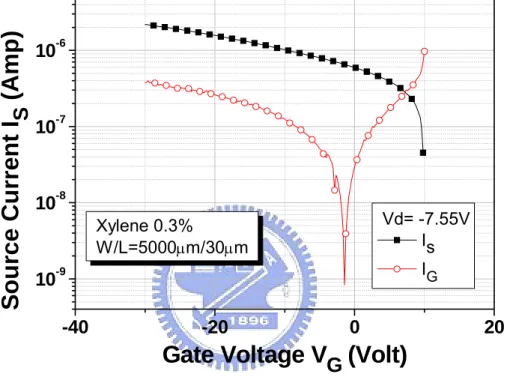
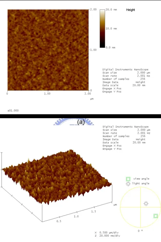
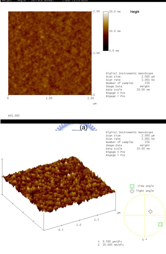
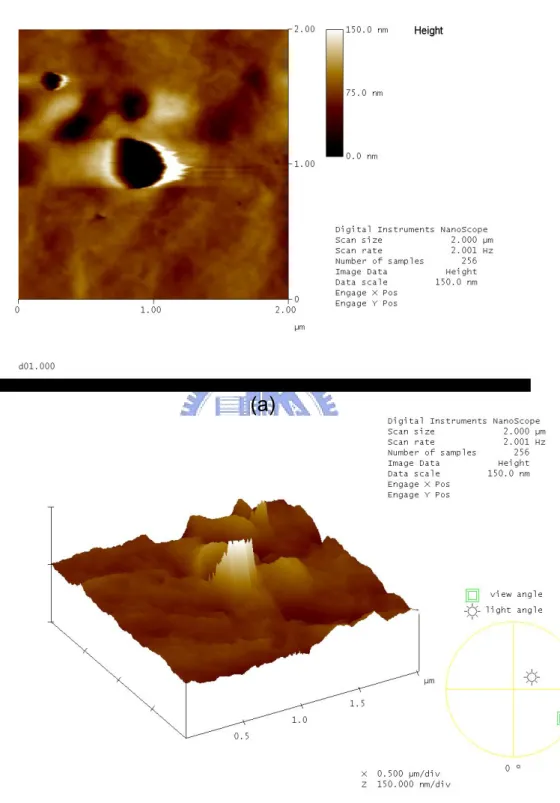
(33) by plotting IDS versus VG at a constant low VD, with -VD << -(VG - VT), and equating the value of the slope of this plot to gm. We can compute the linear regime mobility from equation 2-2. 2.5 OTFTs Fabrication by Different Solvents 2.5.1 Experiment Detail The detailed process flow of P3HT OTFTs fabrication was described in section2.3.1. The different portion is that we prepared different solvents including xylene and chloroform to dissolve P3HT material. Specifically, the P3HT films were deposited from a solution of 0.3% P3HT in xylene or 0.3% P3HT in chloroform. And then the P3HT solution was filtered by a 0.2-µm pore-size PTFE filter and spun onto the wafer surface.. 2.5.2 Result and Discussion 2.5.2.1 Physical properties of spin-on P3HT film We used atomic force microscope to observe the surface morphology and topography of the deposited P3HT film. Fig2-7 exhibits the surface morphology of the deposited P3HT film with different solvents. Fig2-7(a) shows that many clusters of undissolved P3HT powder, despite being filtered, still can be observed, implying that xylene is not a good solvent for P3HT. But from Fig2-7(b), we can not find apparent clusters of undissolved P3HT powder. It follows that chloroform is a good solvent to dissolve P3HT material. Additionally, no apparent grain or grain-boundary structure was found in the AFM photograph because the P3HT thin film is a long-chain polymer.. 2.5.2.2 The anomalous gate leakage current effect from xylene solution. 17.
(34) Current-voltage characteristics of OTFTs were measured in the air with a semiconductor parameter analyzer HP4156. Fig2-8 illustrates source current (IS) and gate leakage current (IG) versus gate voltage where the P3HT OTFT was fabricated by 0.3% xylene solution. The OTFT was turned ON, and the “ON-current” was larger than the gate leakage current by one order. The gate leakage current was comparable to the source current when the device is nearly turned OFF, and finally the gate leakage current dominated the drain current. Due to anomalous gate leakage effect, we cannot measure the ideal I-V characteristics. As a result, the ON-OFF ratio would be affected by anomalous gate leakage current.. Fig2-9(a) shows source current versus drain voltage, where the P3HT OTFT was fabricated by 0.3% xylene solution. Fig2-9(b) shows source current versus drain voltage, where the P3HT OFTF was fabricated by 0.3% chloroform solution. Because of anomalous gate leakage current, the source current at zero bias was above 10-7 Amp as shown in Fig2-9(a). If the solvent was changed from xylene to chloroform, we could not observe apparent anomalous gate leakage current. From Fig2-9(b), the source current at zero bias was below 10-8Amp.Therefore, the anomalous gate leakage current was suppressed by chloroform solution. Because the anomalous leakage current is comparable to the source current of the OTFT with small W/L ratio, the result would be incorrect. Therefore, as the P3HT OTFT was fabricated by 0.3% xylene solution, the anomalous gate leakage current not only influenced the magnitude of source current at zero drain bias, but also the ON-OFF ratio with small W/L. From Fig2-10, if the P3HT OTFT was fabricated by 0.3% xylene solution, ON-OFF ratio was dependent on W/L ratio. But the solvent was changed from xylene to chloroform, the anomalous gate leakage current was suppressed. From Fig2-10, if the P3HT OTFT was fabricated by 0.3% chloroform solution, ON-OFF ratio was independent on W/L ratio.. 18.
(35) 2.5.2.3 The correlation between field-effect mobility of P3HT OTFT and solvent The choice of solvents has a very significant impact on the field-effect mobility of P3HT OTFTs. In a recent publication, Bao et al. [12] observed that chloroform was used as a solvent and P3HT organic semiconductor layer was deposited by spin-coating, the field-effect mobility of P3HT OTFT is about 10-3 cm2/Vs. Xylene was used as a solvent and P3HT organic semiconductor layer was deposited by spin-coating, the field-effect mobility of P3HT OTFT is about 10-4 cm2/Vs, as shown in Table2-2. From Fig2-11, the field-effect mobility of P3HT OTFT which was fabricated by xylene is about 10-3 cm2/Vs and the field-effect mobility of P3HT OTFT which was fabricated by chloroform solution is about 10-4 cm2/Vs. The conclusion was in consistent with the publication [12].. 2.6 OTFTs Fabrication by Different Weight Percentages of P3HT 2.6.1 Experiment Detail In this section, we prepared 0.1%, 0.3%, 0.8%, and 2.0% of P3HT in chloroform. And then the P3HT solution was filtered by a 0.2-µm pore-size PTFE filter and then spun onto the wafer surface. Next, we investigated the electrical characteristics of P3HT OTFTs, such as mobility, threshold voltage and on/off ratio, with different weight percentages of P3HT. Besides, we compared the performance of P3HT OTFTs which were fabricated by new and old P3HT material. New P3HT material, specifically “fresh” P3HT material, means that we purchased it from Aldrich chemical company and were used at once. Old P3HT, although purchased from the same company, had been opened and the remaining chemicals had been storing in air for a year.. 2.6.2 Result and Discussion. 19.
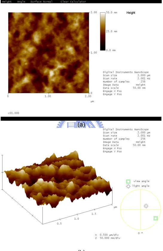
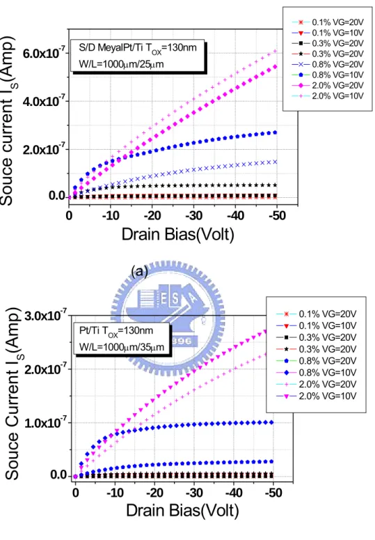
(36) 2.6.2.1 Physical properties of spin-on P3HT film We used atomic force microscope to observe the surface morphology and topography of deposited P3HT film. Fig2-12~Fig2-15 exhibits the surface morphology of the deposited P3HT film with different weight percentage of 0.1%, 0.3%, 0.8% and 2.0% of P3HT in chloroform. It was found that the deposited films by the low weight percentage of P3HT, such as 0.1% and 0.3%, were very smooth, but the deposited films by high weight percentage of P3HT, such as 0.8% and 2.0%, were very rough. When the weight percentage of P3HT as high as 2.0%, there were apparent pinholes in the deposited film. Table2-3 summarized the surface roughness of P3HT film with respect to weight percentage of P3HT in chloroform. The surface root-mean-square roughness of organic thin film deposited by 0.3% of P3HT is 8.24Å. That is much smoother than RMS roughness of organic thin film deposited in other weight percentages.. 2.6.2.2 The bulk current effect from high weight percentage of P3HT There are two current paths in organic semiconductor layer[13]. One is the channel current (Ich), it comes from source electrode (Pt) and goes through the accumulation holes and into drain electrode (Pt). Using established metal-oxide-field effect transistor (MOSFET) current-voltage relationships, the channel current can be written as: I ch =. W µCi (VG − Vth − VD / 2)VD L. as VD << VG − Vth. [Equation 2-3]. for the linear regime, where L is the channel length, W is the channel width, Ci is the capacitance per unit area of the insulating layer, Vth is the threshold voltage, and μ is the field effect mobility. Another leakage path is the bulk current (Ibk). It comes from source electrode (Pt) and goes through conductive layer which is above the accumulation holes and into drain electrode. The bulk current (Ibk) can be represented as 20.
(37) I bk = µ ×. W × l × VDS L. [Equation 2-4]. , where l is the organic semiconductor layer thickness [13]. The P3HT OTFTs were turned ON in the accumulation mode (VG<0, see Fig1-2(b)) and were turned OFF in the depletion mode (VG>0, see Fig1-2(c)). Fig2-16 shows a typical source current versus drain voltage plot at various gate voltages in both accumulation [Fig.2-16(a)] and depletion [Fig.2-16(b)] modes. Fig2-17 is the same. As the positive voltage increases, the source current decreases. It was shown that the device could be turned OFF. But from Fig2-18, IS versus VD curve in the depletion mode as a function of weight concentration of P3HT in chloroform, the devices which were fabricated by 0.8%, 2.0 % of P3HT can not be turned OFF. From two aspects of observation, it can be shown that the current is the bulk current. (1) As the organic semiconductor layer thickness increases, the source current increases. (2) As the drain voltage increases, the source current increases. These conclusions are consistent with Equation 2-4. Either new or old P3HT material, the OTFTs fabricated by high weight percentage of P3HT such as 0.8% and 2.0% can not be observed the ideal IS-VG characteristics as shown in. Fig2-19~Fig2-20 due to the bulk current effect. As a result, threshold voltage and ON-OFF ratio would be affected by the bulk current. Fig2-21 and Fig2-22 shows that threshold voltage as a function of weight concentration of P3HT in chloroform. Because of the bulk current effect there is a dramatic increase as weight concentration of P3HT is above 0.3%.. 2.6.2.3 The correlation between the performances of P3HT OTFT and weight percentage of P3HT For OTFTs fabricated by fresh P3HT material, the following phenomenon can be observed: (1) Fig2-22 illustrates the dependence of threshold voltage and various weight percentages of. 21.
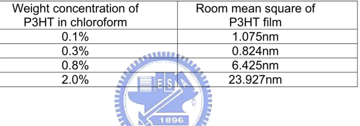
(38) P3HT. The most appropriate wt% of P3HT is 0.1%-0.3%. (2) Fig2-23 illustrates that the field-effect mobility (weight %) dependence shows a maximum at 0.3%-0.8%. (3) Fig2-24 illustrates that ON-OFF ratio (weight %) dependence show a maximum at 0.1%-0.3%. OTFTs fabricated by 0.8 % of P3HT had a better mobility than the others, such as 0.1%, 0.3%, 2.0%, but they can not have an ideal IS-VG characteristic. Therefore, in order to acquire an OTFT with good mobility, high ON-OFF ratio as well as appropriate threshold voltage, the optimal weight percentage of P3HT would be 0.3%. For OTFTs fabricated by old P3HT material, the foregoing phenomenon could not be observed, except threshold voltage, as shown in Fig2-21, Fig2-25 and. Fig2-26. Although similar trends of field-effect mobility and ON-OFF current ratio could not be observed in these figures, the OTFTs fabricated by high weight percentage of P3HT such as 0.8% and 2.0% can not be observed the ideal IS-VG characteristics, which is the same with fresh material.. 2.7 Summary It was found that chloroform is a good solvent to dissolve P3HT, the anomalous gate leakage current was suppressed by chloroform solution, and the high ON-OFF ratio of about four orders of magnitude and the field-effect mobility of 10-3 cm2/Vs were attributed to chloroform solution. The surface root-mean-square roughness of organic thin film deposited by 0.3% of P3HT is 8.24Å. That is much smoother than RMS roughness of organic thin film deposited by others, 0.1%, 0.8% and 2.0%. As weight percentage of P3HT in chloroform is above 0.3%, the bulk current effect would affect IS-VG curves and IS-VD curves. Therefore, in order to acquire an OTFT with good mobility, high ON-OFF current, appropriate threshold voltage, the optimal weight. 22.
(39) percentage of P3HT would be 0.3%.. 23.
(40) Figure 2-1: Chemical diagram of the polymer poly (3-hexylithiophene).R represents the alkyl chain. 24.
(41) Figure2-2:Bottom-contact structure of P3HT OTFTs. 25.
(42) Figure2-3:Process flow of bottom-contact OTFTs. 26.
(43) Egde-on orientation. Face-on orientation Figure2-4: Two different orientations of ordered P3HT domains with respect to the FET substrate [9]. 27.
(44) (a). Source. Drain. (b) Figure2-5: Layouts of bottom-contact OTFTs (a) linear type (b) finger type. 28.
(45) (I L/W Amp) norm S Normalized Source Current I. 10000/10 5000/10 1000/10 1000/15 1000/25 1000/35 1000/50 500/15 500/25 300/35 500/35 500/50. -7. 10. -8. 10. -9. 10. -10. 10. -11. 10. -12. 10. -13. 10. -14. 10. -40 -30 -20 -10. 0. 10. 20. Gate Voltage VG(volt). 30. 40. Fig2-6: Normalized drain-source current vs gate voltage. 29.
(46) (a). (b) Figure2-7:AFM micrograph of P3HT 0.3% in (a) xylene (b) chloroform. 30.
(47) Source Current IS (Amp). -6. 10. -7. 10. -8. 10. Vd= -7.55V Is. Xylene 0.3% W/L=5000µm/30µm. IG. -9. 10. -40. -20. 0. 20. Gate Voltage VG (Volt). Figure 2-8: Source and gate leakage current versus gate bias. 31.
(48) 4.0x10. Source current Is (Amp). VG = 0V. Xylene 0.3% W/L=1000/50µm. -7. VG =-15V VG =-30V. -7. 3.5x10. -7. 3.0x10. -7. 2.5x10. -7. 2.0x10. -7. 1.5x10. -7. 1.0x10. -8. 5.0x10. 0.0 0. -10. -20. -30. -40. -50. -60. Drain bias (V). Souce Current IS(Amp). (a). -7. 3.5x10. VG= 0V VG= -15V VG= -25V. Chloroform 0.3% W/L=1000/50µm. -7. 3.0x10. -7. 2.5x10. -7. 2.0x10. -7. 1.5x10. -7. 1.0x10. -8. 5.0x10. 0.0 0. -10. -20. -30. -40. Drain Bias(Volt) (b). Figure2-9:Influence of gate leakage current on output characteristics IS vs VD:(a) xylene 0.3% (b) chloroform 0.3%. 32.
(49) 4. On-Off Ratio. 10. 3. 10. Xylene 0.3% Chloroform 0.3%. 2. 10. 1. 10. 0. 200. 400. 600. 800. 1000. W/L. Figure2-10: On-Off ratio versus W/L. 33.
(50) Source Current IS(A). -6. 3.0x10. -3. 2.5x10. -3. 2.0x10. -3. 1.5x10. -3. 1.0x10. -3. 5.0x10. -4. Mobility µ (10 cm /Vs). Chloroform 0.3% Xylene 0.3%. -5. 10 10. -7. 10. W/L=10000/10µm -9. 10. 0.0. -10. 10. 2. Ti/Pt Tox=150nm. -3. -8. 10. -40. -30. -20. -10. 0. 10. 20. 30. 40. Gate Voltage VG(volt). (a) Chloroform 0.3% Xylene 0.3%. -3. 5.0x10. -5. W/L=5000/10µm. -3. 4.0x10. -7. 10. -3. 3.0x10 -5. 6.0x10. -3. 2.0x10. -3. 2. -9. 10. Mobility µ (10 cm /Vs). -8. 10. -5. 3.0x10. -11. 10. -12. 10. 2. -10. 10. -40. -30. -3. Source Current IS(A). Ti/Pt Tox=150nm. -6. 10. Mobility µ (10 cm /Vs). 10. -3. 1.0x10 0.0 -40. -20. -20. -10. 0. 20. 0. 40. 10. 0.0. 20. 30. 40. Gate Voltage VG(volt). (b) Figure2-11: Transfer characteristics IS vs VG and field-effect mobility of samples prepared from different solvrnt (a) W/L=10000/10 µm (b) W/L=5000/10 µm (c) W/L=1000/10 µm (d) W/L=1000/50 µm (continue). 34.
(51) -7. -3. 10. Source Current IS(A). Mobility µ (10 cm /Vs). Chloroform 0.3% Xylene 0.3%. -6. 10. 2.0x10. -8. 10. -3. Ti/Pt Tox=150nm W/L=1000/10µm. -9. 10. -3. 1.0x10. 2. -10. 10. -11. 10. -40. -30. -20. -10. 0. 10. 20. 30. 0.0 40. Gate Voltage VG(volt). (c) -6. -2. Source Current IS(A). 2.0x10 Chloroform 0.3% Xylene 0.3%. -2. 1.6x10. -7. 10. Mobility µ (10 cm /Vs). 10. -2. 1.2x10 -8. -3. 10. -3. 8.0x10 Ti/Pt Tox=150nm W/L=1000/50µm. 2. -9. 10. -3. 4.0x10. -10. 10. -40. 0.0. -30. -20. -10. 0. 10. 20. 30. 40. Gate Voltage VG(volt). (d) Figure2-11: Transfer characteristics IS vs VG and field-effect mobility of samples prepared from different solvent (a) W/L=10000/10 µm (b) W/L=5000/10 µm (c) W/L=1000/10 µm (d) W/L=1000/50 µm. 35.
(52) (a). (b) Figure 2-12: AFM micrograph of P3HT 0.1% in chloroform (a) top-view (b) high angle view. 36.
(53) (a). (b) Figure 2-13:AFM micrograph of P3HT 0.3% in chloroform (a) top-view (b) high angle view. 37.
(54) (a). (b) Figure 2-14: AFM micrograph of P3HT 0.8% in chloroform (a) top-view (b) high angle view. 38.
(55) (a). (b) Figure 2-15:AFM micrograph of P3HT 2.0% in chloroform (a) top-view (b) high angle view. 39.
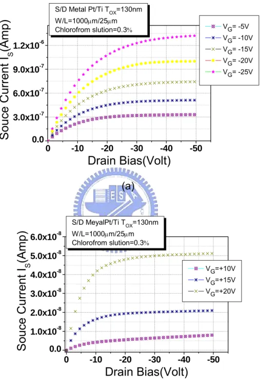
(56) S/D Metal Pt/Ti TOX=130nm. Souce Current IS(Amp). W/L=1000µm/25µm Chlorofrom slution=0.3%. VG= -5V VG= -10V. -6. 1.2x10. VG= -15V VG= -20V. -7. 9.0x10. VG= -25V. -7. 6.0x10. -7. 3.0x10. 0.0 0. -10. -20. -30. -40. -50. Drain Bias(Volt) (a). Souce Current IS(Amp). S/D MeyalPt/Ti TOX=130nm W/L=1000µm/25µm Chlorofrom slution=0.3%. -8. 6.0x10. -8. 5.0x10. VG=+10V. -8. 4.0x10. VG=+15V VG=+20V. -8. 3.0x10. -8. 2.0x10. -8. 1.0x10. 0.0 0. -10. -20. -30. -40. -50. Drain Bias(Volt) (b) Figure 2-16: IS versus VD curve at different gate voltages (a) in the accumulation mode (b) in the depletion mode (W/L=1000/25µm). 40.
(57) Souce Current IS(Amp). S/D Metal Pt/Ti TOX=130nm W/L=1000µm/35µm Chlorofrom slution=0.3%. -7. VG=-5V VG=-10V. 1.2x10. VG=-15V VG=-20V VG=-25V. -8. 8.0x10. -8. 4.0x10. 0.0 0. -10. -20. -30. -40. -50. Drain Bias(Volt) (a). Souce Current IS(Amp). Pt/Ti TOX=130nm W/L=1000µm/35µm Chlorofrom slution=0.3%. -9. 6.0x10. -9. 5.0x10. VG=+10V. -9. VG=+15V. 4.0x10. VG=+20V. -9. 3.0x10. -9. 2.0x10. -9. 1.0x10. 0.0 0. -10. -20. -30. -40. -50. Drain Bias(Volt) (b) Figure2-17: IS versus VD curve at different gate voltages (a) in the accumulation mode (b) in the depletion mode (W/L=1000/35µm). 41.
(58) Souce current IS(Amp). 0.1% VG=20V 0.1% VG=10V 0.3% VG=20V 0.3% VG=20V 0.8% VG=20V 0.8% VG=10V 2.0% VG=20V 2.0% VG=10V. S/D MeyalPt/Ti TOX=130nm. -7. 6.0x10. W/L=1000µm/25µm. -7. 4.0x10. -7. 2.0x10. 0.0 0. -10. -20. -30. -40. -50. Drain Bias(Volt). Souce Current IS(Amp). (a) -7. 0.1% VG=20V 0.1% VG=10V 0.3% VG=20V 0.3% VG=20V 0.8% VG=20V 0.8% VG=10V 2.0% VG=20V 2.0% VG=10V. 3.0x10. Pt/Ti TOX=130nm W/L=1000µm/35µm -7. 2.0x10. -7. 1.0x10. 0.0 0. -10. -20. -30. -40. -50. Drain Bias(Volt) (b) Figure 2-18: IS versus VD curve in the depletion mode as a function of weight concentration of P3HT in chloroform (a) W/L=1000/25µm (b) W/L=1000/35µm. 42.
(59) Old material W/L=10000/10µm. -4. 10. Source Current IS(A). -5. 10. -6. 10. 0.1% VDS=-5V 0.3% VDS=-5V. -7. 10. 0.8% VDS=-5V -8. 2.0% VDS=-5V. 10. -9. 10. -10. 10. -40. -30. -20. -10. 0. 10. 20. 30. 40. Gate Voltage VG(volt). (a) Old material W/L=1000/35µm. -6. 10. Source Current IS(A). -7. 10. -8. 10. 0.1% VDS=-5V. -9. 10. 0.3% VDS=-5V 0.8% VDS=-5V. -10. 10. 2.0% VDS=-5V. -11. 10. -12. 10. -30. -20. -10. 0. 10. 20. 30. 40. Gate Voltage VG(volt). (b) Figure2-19: Transfer characteristics IS vs VG as a function of weight concentration of P3HT in chloroform: (a)W/L=10000/10µm (b)W/L=1000/35µm (c)W/L=500/15µm (d)W/L=500/25µm (continue). 43.
(60) -5. 10. Old material W/L=500/15µm. -6. Source Current IS(A). 10. -7. 10. -8. 10. 0.1% VDS=-5V. -9. 10. 0.3% VDS=-5V 0.8% VDS=-5V. -10. 10. 2.0% VDS=-5V. -11. 10. -12. 10. -30. -20. -10. 0. 10. 20. 30. 40. Gate Voltage VG(volt). (c). Old material W/L=500/25µm. -6. Source Current IS(A). 10. -7. 10. -8. 10. 0.1% VDS=-5V. -9. 0.3% VDS=-5V. 10. 0.8% VDS=-5V. -10. 10. 2.0% VDS=-5V. -11. 10. -30. -20. -10. 0. 10. 20. 30. 40. Gate Voltage VG(volt). (d) Figure2-19: Transfer characteristics IS vs VG as a function of weight concentration of P3HT in chloroform: (a)W/L=10000/10µm (b)W/L=1000/35µm (c)W/L=500/15µm (d)W/L=500/25µm. 44.
(61) -4. 10. New material W/L=10000/10µm. Source Current IS(A). -5. 10. -6. 10. -7. 10. 0.1% VDS=-5V. -8. 10. 0.3% VDS=-5V. -9. 10. 0.8% VDS=-5V 2.0% VDS=-5V. -10. 10. -11. 10. -40. -30. -20. -10. 0. 10. 20. Gate Voltage VG(volt). 30. 40. (a) -5. 10. New material W/L=1000/15µm. -6. Source Current IS(A). 10. -7. 10. -8. 10. 0.1% VDS=-5V. -9. 10. 0.3% VDS=-5V 0.8% VDS=-5V. -10. 10. 2.0% VDS=-5V. -11. 10. -12. 10. -40. -30. -20. -10. 0. 10. 20. 30. 40. Gate Voltage VG(volt). (b) Figure2-20: Transfer characteristics IS vs VG as a function of weight concentration of P3HT in chloroform: (a) W/L=10000/10µm (b) W/L=1000/15µm (c) W/L=1000/35µm (d) W/L=500/15µm (e) W/L=500/25µm (continue). 45.
(62) -5. 10. New material W/L=1000/35µm. -6. Source Current IS(A). 10. -7. 10. -8. 10. 0.1% VDS=-5V. -9. 10. 0.3% VDS=-5V. -10. 10. 0.8% VDS=-5V 2.0% VDS=-5V. -11. 10. -12. 10. -40. -30. -20. -10. 0. 10. 20. 30. Gate Voltage VG(volt). 40. (c) -5. 10. New material W/L=500/15µm. -6. Source Current IS(A). 10. -7. 10. -8. 10. 0.1% VDS=-5V. -9. 10. 0.3% VDS=-5V. -10. 10. 0.8% VDS=-5V 2.0% VDS=-5V. -11. 10. -12. 10. -40. -30. -20. -10. 0. 10. 20. Gate Voltage VG(volt). 30. 40. (d) Figure2-20: Transfer characteristics IS vs VG as a function of weight concentration of P3HT in chloroform: (a) W/L=10000/10µm (b) W/L=1000/15µm (c) W/L=1000/35µm (d) W/L=500/15µm (e) W/L=500/25µm (continue). 46.
(63) New material W/L=500/25µm. -6. Source Current IS(A). 10. -7. 10. -8. 10. 0.1% VDS=-5V. -9. 10. 0.3% VDS=-5V 0.8% VDS=-5V. -10. 10. 2.0% VDS=-5V. -11. 10. -40. -30. -20. -10. 0. 10. 20. Gate Voltage VG(volt). 30. 40. (e) Figure2-20: Transfer characteristics IS vs VG as a function of weight concentration of P3HT in chloroform: (a) W/L=10000/10µm (b) W/L=1000/15µm (c) W/L=1000/35µm (d) W/L=500/15µm (e) W/L=500/25µm. 47.
(64) Threshold Voltage (Volt). 240. Old material. 200 160 120 W/L=10000/10µm W/L=1000/35µm W/L=500/15µm W/L=500/25µm. 80 40 0. 0.0 0.5 1.0 1.5 2.0 P3HT weight % in Chloroform(%). Figure2-21: Threshold voltage as a function of weight concentration of P3HT in chloroform. 48.
(65) Threshold Voltage (Volt). 200. New material. 160 120 80. W/L=10000/10µm W/L=1000/15µm W/L=1000/25µm W/L=1000/35µm. 40 0. 0.0 0.5 1.0 1.5 2.0 P3HT weight % in Chloroform(%). Threshold Voltage (Volt). (a) 250 New material. 200 150 100. W/L=500/15µm W/L=500/25µm. 50 0. 0.0 0.5 1.0 1.5 2.0 P3HT weight % in Chloroform(%). (b) Figure2-22: Threshold voltage as a function of weight concentration of P3HT in chloroform: (a) inter-digital type (b) linear type. 49.
(66) 8. 2. Mobility µ (10 cm /Vs). W/L=10000/10µm W/L=1000/15µm W/L=1000/25µm W/L=1000/35µm. New material. -3. 6 4 2 0. 0.0 0.5 1.0 1.5 2.0 P3HT weight % in Chloroform(%). -3. 2. Mobility µ (10 cm /Vs). (a) 10. New material. 8 6 4 W/L=500/15µm W/L=500/25µm. 2 0. 0.0 0.5 1.0 1.5 2.0 P3HT weight % in Chloroform(%). (b) Figure2-23: Field-effect mobility in the linear regime as a function of weight concentration of P3HT in chloroform : (a) inter-digital type (b) linear type. 50.
(67) 5. 10. New material. On-Off Ratio. 4. 10. 3. 10. 2. 10. 1. 10. W/L=10000/10µm W/L=1000/15µm W/L=1000/25µm W/L=1000/35µm. 0. 10. -1. 10. 0.0 0.5 1.0 1.5 2.0 P3HT weight % in Chloroform(%). (a) 5. 10. New material. 4. On-Off Ratio. 10. 3. 10. 2. 10. 1. 10. 0. 10. W/L=500/15µm W/L=500/25µm. -1. 10. 0.0 0.5 1.0 1.5 2.0 P3HT weight % in Chloroform(%). (b) Figure2-24: On-off ratio as a function of weight concentration of P3HT in chloroform : (a) inter-digital type (b) linear type. 51.
(68) Old material. 10. 2. Mobility µ (10 cm /Vs). 12. -3. 8 6 4. W/L=10000/10µm W/L=1000/35µm W/L=500/15µm W/L=500/25µm. 2 0. 0.0 0.5 1.0 1.5 2.0 P3HT weight % in Chloroform(%). Figure2-25: Field-effect mobility in the linear regime as a function of weight concentration of P3HT in chloroform. 52.
(69) 5. 10. Old material. 4. On_Off Ratio. 10. 3. 10. 2. 10. 1. 10. 0. 10. W/L=10000/10µm W/L=1000/35µm W/L=500/15µm W/L=500/25µm. -1. 10. 0.0 0.5 1.0 1.5 2.0 P3HT weight % in Chloroform(%). Figure2-26: On-off ratio as a function of weight concentration of P3HT in chloroform. 53.
(70) INO(Amp). Off current(Amp). W/L=10000/10μm. 1.00E-12. 1.00E-09. W/L=5000/10μm. 1.00E-12. 5.00E-10. W/L=1000/10μm. 1.00E-12. 1.00E-10. W/L=1000/15μm. 1.00E-12. 6.60E-11. W/L=1000/25μm. 1.00E-12. 4.00E-11. W/L=1000/35μm. 1.00E-12. 2.80E-11. W/L=1000/50μm. 1.00E-12. 2.00E-11. W/L=500/10μm. 1.00E-12. 5.00E-11. W/L=500/15μm. 1.00E-12. 3.30E-11. W/L=500/25μm. 1.00E-12. 2.00E-11. W/L=500/35μm. 1.00E-12. 1.40E-11. W/L=500/50μm. 1.00E-12. 1.00E-11. W/L=300/35μm. 1.00E-12. 8.50E-12. W/L. Table2-1: The magnitude of off current with different channel length and different channel width. 54.
(71) Table2-2: Field-effect mobility and ON/OFF ratios of samples prepared from different conditions Condition 1:cast, vacuum pumped for 24 h; condition 2: spin-coated; condition 3: treated with NH3 for 10 h; condition 4:heated to 100 °C under N2 for 5 min; condition 5: heated to 150 °C under N2 for 35 min.. 55.
(72) Weight concentration of P3HT in chloroform 0.1% 0.3% 0.8% 2.0%. Room mean square of P3HT film 1.075nm 0.824nm 6.425nm 23.927nm. Table 2-3: Room mean square of P3HT film as a function of weight concentration of P3HT in chloroform. 56.
(73) Chapter 3 Reliability Characteristics of P3HT OTFTs. 3.1 Introduction Organic electronics has been a subject of increasing interest. One of the materials used for organic thin film transistors is poly (3-hexylthiophenes), P3HT. In the last few years, the main object on P3HT OTFTs is to improve the carrier mobility. Therefore, the performance of P3HT OTFTs has improved remarkably through optimization of process parameters and is comparable to amorphous silicon thin film transistors (a-TFTs) [5], [14]. Besides, OTFTs exhibit great potential for special applications such as flexible display, RF tags, and smart cards. However, comparing to inorganic transistors, organic devices show poor stability with time and different environmental ambient such as nitrogen, oxygen or moisture may affect the performance of organic devices [13], [15]. Therefore, stability issues of these organic devices are another challenge which should be kept in mind. Several reports have indicated that P3HT OTFTs are sensitive to the presence of oxygen [13], [15]. Additionally, in our previous work we also observed obvious degradation of threshold voltage, mobility or ON/OFF current ratios of OTFTs after exposing devices in the air for several days. Thus, we treated OTFTs with O2, N2 and H2O deliberately to clarify the correlation between electrical characteristics of P3HT OTFTs and the exposed ambient. For organic devices, although there have been tremendous progress on prerequisites such as device fabrication and material optimization, studies of the operational lifetime have been scarce up to now [17]. Therefore, we investigate the behavior of P3HT OTFTs during stress. 57.
(74) measurements.. 3.2 The Effect of P3HT OTFTs Stored in Vacuum 3.2.1 Experiment Detail As discussed in chapter 2, a good solvent to dissolve P3HT is chloroform and the optimal weight percentage of P3HT is 0.3%. Afterward, we used this condition to deposit organic semiconductor layer in the following experiments. The other detailed process flow of P3HT OTFTs fabrication was described in section 2.3.1. Notably, all of the processing steps were carried out under clean room conditions in the presence of ambient oxygen and relative humidity about 60%. In this section, we prepared two samples. One was measured immediately in the air with semiconductor parameter analyzer HP4156 after the P3HT OTFTs were fabricated; the other one was stored in a high vacuum chamber with base pressure of 1×10⁻⁶ torr for 2 days after P3HT OTFT was fabricated, and then the sample was measured immediately in the air after being stored in vacuum.. 3.2.2 Results and Discussion Several reports have indicated that P3HT polymer is sensitive to the presence of oxygen [18], [19]. It has been shown that oxygen is a kind of dopant for P3HT polymer. Moreover, if there are oxygen atoms in P3HT polymer, carriers scattering would occur and the field-effect mobility would decrease. Since our P3HT OTFTs were not fabricated in vacuo, the influence of oxygen to the characteristics of organic transistors is inevitable. Therefore, we employ vacuum storage to check the significance of oxygen auto-doping and whether the vacuum storage can. 58.
(75) eliminate the effect of oxygen doping or not. As can be seen from Table3-1~Table3-3 and Figure3-1, the field-effect mobility of devices were further improved by storing the sample for 2days in high vacuum chamber before electrical measurements as the maximum field-effect mobility reaches 10-2 cm2/Vs. Additionally, threshold voltage of devices were greatly decreased and ON-OFF ratios were improved by storing the sample for 2days in high vacuum chamber before electrical measurements. The above results are in consistent with those reported in literatures [20], [21] and verified that oxygen does affect the electrical characteristics of P3HT OTFTs. Based on the above observation, our OTFT devices would be stored in high vacuum chamber for 2 days before electrical measurement in order to acquire a stable P3HT polymer film.. 3.3 The Variation of Threshold Voltage and Field-Effect Mobility during the Electrical Measurement 3.3.1 Experiment Detail After the P3HT OTFTs had been fabricated, devices would be measured by Agilent 4156c within 60 minutes. In order to observe the variation of field-effect mobility and threshold voltage during the electrical measurement, we measured the same device repeatedly after 10sec, 30sec, 80sec, 180sec, 380sec, 880sec, 1880sec, 3880sec and 8880sec.. 3.3.2 Results and Discussion Fig3-2 indicates that the variation of field-effect mobility and threshold voltage within 120min of measurement. For first 60 min, the variation of field-effect mobility is insignificant,. 59.
數據
![Figure 1-1:Semilogarithmic plot of the highest field-effect mobility(µ) reported for OTFTs fabricated from the most promising polymeric and oligomeric semiconductors versus year from 1986 to 2000.[1]](https://thumb-ap.123doks.com/thumbv2/9libinfo/8516698.186227/22.892.207.729.275.819/semilogarithmic-mobility-reported-fabricated-promising-polymeric-oligomeric-semiconductors.webp)

+7
相關文件
Chou, “The Application on Investigation of Rice Field Using the High Frequency and High Resolution Satellite Images (1/3)”, Agriculture and Food Agency, 2005. Lei, “The Application
(1. International arts organization: A foundation, association, company, group, or unit whose mission is geared toward culture or the arts. Examples include the American Theatre
Miners in England used horses to pull heavy carts or cars of coal or iron on wooden tracks out of the mines.. With these tracks, the horses could pull twice as much weight as
雙極性接面電晶體(bipolar junction transistor, BJT) 場效電晶體(field effect transistor, FET).
Analysis Based on Xia Jing Shan’s Seven Sages of Bamboo Grove: Comparing the sacred and the profane, by using symbols as a connector, profane occurrences and things could then
DWI findings of thyroglossal duct cysts were not similar to those of ranulas, as 2 of the 3 lesions had heterogeneous high signal intensity (see Figure 3 and Table
As the increase in expenditure exceeded that in receipts, these hotels recorded a deficit of MOP 619 million, while Gross Surplus Ratio went down by 12.4 percentage points
Due to a definition of noise factor (in this case) as the ratio of noise powers on the output versus on the input, when a resistor in room temperature ( T 0 =290 K) generates the
