國 立 交 通 大 學
電信工程學系
碩 士 論 文
一個低功率的權重前饋控制串聯式積分器架構
之二階三角積分器設計與實現
Design and Implementation of a Low-Power CIFF
Structure Second-Order Sigma-Delta Modulator
研究生:蘇品翰
指導教授:闕河鳴 博士
之二階三角積分器設計
Design and Implementation of a Low-Power CIFF Structure
Second-Order Sigma-Delta Modulator
研 究 生:蘇品翰 Student: Pin-Han Su
指導教授:闕河鳴 博士 Advisor: Dr. Herming Chiueh
國 立 交 通 大 學
電 信 工 程 學 系 碩 士 班
碩 士 論 文
A Thesis
Submitted to Department of Communication Engineering College of Electrical and Computer Engineering
National Chiao Tung University in Partial Fulfillment of the Requirements
for the Degree of Master of Science in Communication Engineering January 2009 Hsinchu, Taiwan 中 華 民 國 九 十 八 年 一 月
I
一個低功率的權重前饋控制串聯式積分器架構
之二階三角積分器設計
研究生:蘇品翰 指導教授:闕河鳴 博士 國立交通大學 電信工程學系碩士班摘要
隨著 VLSI 技術的演進,類比電路已經被實現在更低的提供電壓及更小的晶片 面積。在各種低供電、低功率消耗的元件中,三角積分數位類比轉換器在音頻的 可攜帶電子元件應用上的實現,是一種比起其他數位類比轉換器、在功率消耗上 更有效率的一種實現方式。 本論文提出並經由台積電的 0.18 微米製程實現了一個低功率消耗的三角積分 數位轉換器電路。經由將回路濾波器中的運算跨導放大器的規格做最佳化,一個 電流最佳化的技術被提出。使用權重前饋控制串聯式積分器的調變器架構以及單 級-A 類加上正回授的運算跨導放大器電路,本論文提出的三角積分類比數位轉 換調變器的訊號雜訊比到達 63.4dB,並且能處理直流到最高 16KHz 的訊號。使用 一伏特的供應電壓、整個調變器的功率消耗只有 18 微瓦特。II
Design and Implementation of a Low-Power CIFF Structure
Second-Order Sigma-Delta Modulator
Student: Pin-Han Su Advisor: Dr. Herming Chiueh SoC Design Lab, Department of Communication Engineering,
College of Electrical and Computer Engineering, National Chiao Tung University Hsinchu 30010, Taiwan
Abstract
With the scaling down of VLSI technology, the analog circuit have implemented with a lower supply voltage and smaller chip area. Among the low-voltage low-power building blocks, the sigma-delta ADC provides a power-efficient way to implement an ADC for audio-band portable device applications.
This thesis presents the design and implementation of a low power sigma-delta modulator (SDM) with a standard 0.18-μm CMOS technology. A current optimization technique is proposed by making a specification optimization of the Operational Transconductance Amplifier (OTA) in loop filter. Using a chain of Integrators with weighted feed-forward summation (CIFF) structure and a single-stage class-A OTA with positive feedback, the proposed second-order SDM achieves a SNR of 63.4dB that be able to process the signal form DC to 16KHz.The power consumption is only 18 uW from a 1-V supply.
III
Acknowledgements
本篇碩士論文得以順利完成,首先要感謝的是我的指導教授闕河鳴博士。在 實驗室的日子裡,闕老師總在我研究遇到瓶頸時給予我寶貴的建議,使我找到正 確的研究方向。除此之外、老師平日特別注重學生獨立思考以及分析問題的能 力,使我在研究的領域建立起正確的研究態度。 其次,謝謝嘉儀、順華、江俊、信太及俊誼學長在研究上或是日常生活上對 我的照顧;還要謝謝秉勳、凱迪、明君、春慧四位同學在我的課業及生活上的幫 忙;平常在研究領域上的討論及切磋,讓我的基本觀念能夠更加的紮實。也謝謝 是瑜、鎮宇、國哲、鼎國、燦傑、登政等學弟的支持與幫忙。最後還要特別謝謝 大學同學士豪、奐箴、訓緯、建興、傑天、慶陽、善凡、詠峻、俊穎、士昌等人 對我在類比電路設計領域的幫助。有了各位的陪伴,才能讓我在這兩年半的日子 裡有這麼快樂且充實的研究生活。 最後我要感謝我的父母,以及所有關心我的家人與朋友,謝謝大家的愛護跟 幫忙,讓我能順利的完成學業。 我誠心感謝上述曾提攜或幫助過我的你們,謝謝大家並祝福大家。 蘇品翰 January,8,2009 於新竹
IV
Content
中文摘要
………..…….. I
English Abstract……….. II
Acknowledgement……….
III
Content………....
IV
List of Tables………..
VI
List of Figures………VII
Chapter 1 Introduction……… 1
1.1 Motivation………..……… 1 1.2 Organization………..…….… 3Chapter 2 SDM Fundamentals ………..……… 4
2.1 A brief Introduction of ADC………..………..…4
2.2 Oversampling and Noise Shaping……….………….. 8
2.2.1 Oversampling………..………...8
2.2.2 Noise Shaping………9
2.3 Performance Metrics……….…………. 10
Chapter3 System Considerations……….. 12
3.1 Power Considerations in SDM………12
3.2 System Parameter Considerations………15
3.2.1 Topology Decision………..16
3.2.2 Architecture Selection……….18
3.2.3 Coefficient Decision………20
3.3 Non-idealities Considerations……….24
3.3.1 Gain requirement………24
3.3.2 Settling of the OTA………25
V
Chapter 4 Circuit Implementation………..28
4.1 Transistor Level Design………..28
4.1.1 Differential OTA in loop filter………..28
4.1.2 1-bit quantizer………..38
4.1.3 Clock Generator………..39
4.1.4 Switches………..41
4.2 Modulator Design and Simulation………..42
4.3 Layout Level Design………...45
4.4 Comparison……….49
Chapter 5 Testing Setup and Measurement……….51
5.1 Testing Environment Setup……….51
5.2 Measurement Result………53
5.3 Summary……….56
Chapter 6 Conclusions ……….…….………..57
VI
List of Tables
Table 2.1 various kinds of ADCs...5
Table 3.1 Summary of previous SDM papers………..13
Table 3.2 Specification comparison of OTA .………..14
Table 3.3 Power comparison of different loop filter order………..17
Table 3.4 Coefficient of proposed SDM………..22
Table 4.1 Device ratio summary of first OTA………..34
Table 4.2 Summary of first OTA simulation results……….35
Table 4.3 Performance comparison of the two OTA………35
Table 4.4 Comparison before/after current optimization……….36
Table 4.5 CMFB circuit summary………37
Table 4.6 Quantizer Transistor size summary…………..………39
Table 4.7 Comparison of the simulation results of four corners………..44
Table 4.8 Pin Assignments………..47
Table 4.9 Comparisons of pre and post simulation………….………48
Table 4.10 Summary of proposed SDM……….……….48
Table 4.11 Comparison of this work………49
Table 5.1 Output buffer device ratio summary………53
Table 5.2 the modified output buffer device ratio summary………54
Table 5.3 Power consumption for three parts circuits………55
VII
List of Figures
Figure 2.1 Block diagram of an ADC………4
Figure 2.2 Transfer curve of ADCs………5
Figure2.3 Power spectral density of quantization noise………6
Figure 2.4 Quantization noise in an oversampled converter………..8
Figure 2.5 A linear model of the sigma-delta modulator………9
Figure 2.6 Performance metrics………...11
Figure 3.1 power consumption in an OTA .………..………....15
Figure 3.2 Chain of Integrators with distributed feedback (CIFB)………..18
Figure 3.3 Chain of integrators with weighted feed-forward summation (CIFF)……19
Figure 3.4 Simulink model of a 2nd-order CIFF SDM……….20
Figure 3.5 a second order CIFF SDM………..21
Figure 3.6 A general linear model of SDM………..21
Figure 3.7 Ideal 8192 point FFT of proposed SDM architecture……….23
Figure 3.8 a switched-capacitance circuit in SDM………..…24
Figure 3.9 Sampling and integration period of a loop filter……….25
Figure 3.10 Settling behavior of OTA………..26
Figure 3.11 Simulation result of the first sampling capacitor………..27
Figure 4.1 Single stage class-A OTA with positive feedback………..29
Figure 4.2 Trade-off between slewing and linear settling………...30
Figure 4.3 Slewing time versus total current of the OTA………31
Figure 4.4 modification of the slewing time………32
Figure 4.5 Current consumption of the first OTA………33
Figure 4.6 Current consumption of the second OTA………..…35
Figure 4.7 Frequency Response of first OTA………..36
Figure 4.8 Dynamic CMFB circuit………..37
Figure 4.9 Transient Response of first OTA output……….37
Figure 4.10 a power-efficient 1-bit quantizer………..38
Figure 4.11 Simulation results of the 1-bit quantizer………..38
Figure 4.12 Clock generator circuit……….39
Figure 4.13 Output of the clock generator………..40
Figure 4.14 Four non-overlapping phases………..40
Figure 4.15 2nd order CIFF SDM………42
Figure 4.16 output signal of input and two integrator outputs………42
VIII
Figure 4.18 Dynamic range of the SDM………..44
Figure 4.19 Diagram of the layout……….…………..…45
Figure 4.20 Diagram of the 24 pin DIP package...46
Figure 4.21 Die photograph……….46
Figure 4.22 8192-point FFT of the post-simulation result……….…………..48
Figure 4.23 SNR versus power consumption comparisons……….50
Figure 5.1 experimental test setup………52
Figure 5.2 Photograph off the measurement environment………...52
Figure 5.3 Probably problem of output buffers………..….53
Figure 5.4 modified version of layout……….……….54
1
Chapter 1
Introduction
1.1 Motivation
With the scaling down of modern VLSI technology in recent years, the digital circuits have implemented with a complex and a higher clock rate, and it introduces more constraints for the analog circuits.
However, the decreased supply voltage restricts the signal swing in circuits and brings difficulties for analog circuit design. In low-voltage environments, the transistor characteristics degrade and some circuit techniques can no longer be used, thus the low-voltage design different from the traditional circuit design technique. Therefore, the design of low-voltage, low-power analog devices has become more and more important.
Among the low-voltage low-power building blocks, the audio-band battery-based operation system is highly desired by various applications, such as mp3 players, radio-frequency identification (RFID), biomedical electronics and digital hearing aid instrument.
In these devices, the analog-to-digital converters (ADCs) are widely used in various systems, because it is necessary to transfer nature analog signal to digital code.
2
Among different ADC topologies, the Sigma-Delta ADCs efficiently trade speed for accuracy, providing an efficient way to implement high-resolution ADCs without stringent matching requirements compared to other types of ADCs (ex: flash ADC, pipeline ADC). By over-sampling and noise shaping, the sigma-delta ADCs transfer most of the signal processing tasks to the digital domain. Therefore, for high-resolution ADCs, the sigma-delta ADCs are more power-effective and robust compared to other architectures.
Therefore, the design target of this thesis is to achieve a low-power audio band sigma-delta ADC design. The experimental SDM present here have been fabricated in a standard 0.18um CMOS technology, and provide a SNR of 63dB for audio band signal (16k) and only dissipates 18uW, it can be used in a low power portable audio devices.
3
1.2 Organization
In Chapter 2, the beginning is the overview of the analog-to-digital converters (ADC). After them, the quantization issues, oversampling and noise shaping are introduced. Then the performance metrics of sigma-delta modulators (SDM) end this chapter.
Chapter 3 describes the system level design considerations, including the analysis of the power issues of SDM, the topology selections and the limitations and non-ideal effects of the SDM.
Chapter 4 discusses the topics of sub-circuits that will be used to realize the proposed SDM circuit, which includes an OTA, a comparator, a clock generator, capacitors and switches. The pre-simulation and post-simulation results are given. The layout level design will be described in this sequence.
In Chapter 5, the testing environment is present, including the instruments and the testing circuits on printed circuit board (PCB).The experimental results for the SDM, which is fabricated in a 0.18um 1P6M 1.8V standard CMOS technology with MIM process will be summarized.
4
Chapter 2
SDM Fundamentals
This chapter begins with a brief overview of analog-digital converter (ADC). Following by the classification of ADC, the oversampling and noise shaping is introduced and considered and defined mathematically. The performance metrics of targeting ADC is than described in the end of this chapter.
2.1 A brief Introduction of ADC
The ADCs are fed a continuous-time analog signal to convert discrete-time digital signals. In order to perform the analog to digital conversion, two steps should be down. The first is the discretization of the continuous analog signal, which is called sampling. After sampling, the quantization step is followed by digitizing the amplitude of the discrete signal, as shown in Figure 2.1.
5
For an ADC, there are two important parameters, input signal bandwidth and resolution, and different types of ADCs are developed according to different input signal bandwidth and resolution requirements as depicted in Table 2.1. Among the ADCs, the sigma-delta ADC is suitable to medium to high resolution applications in the audio frequency range.
Category Structure
Low-to-Medium Speed High Accuracy
Integrating ADC Sigma-Delta ADC
Medium Speed , Medium Accuracy Successive approximation ADC High Speed
Low-to-Medium Accuracy
Pipeline ADC Flash ADC Table 2.1 various kinds of ADCs
Since the process of quantization is a classification process in amplitude, there is always an error in an ADC, and the quantization error e is smaller than the q
quantization stepΔ of the ADC, as depicted in Figure 2.2.
2
e
q2
Δ
Δ
6
Figure 2.2 Transfer curve of ADCs
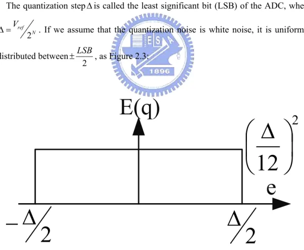
The quantization stepΔ is called the least significant bit (LSB) of the ADC, where
2
ref N
V
Δ = . If we assume that the quantization noise is white noise, it is uniformly distributed between 2 LSB ± , as Figure 2.3:
2
12
⎟
⎠
⎞
⎜
⎝
⎛ Δ
2
Δ
−
Δ
2
7
Therefore, the power of the quantization error can be derived as: 2 2
( )
12
e qP
e
ρ
e de
∞ −∞Δ
=
∫
=
(2.2)For a sinusoidal input signal, its maximum peak value without clipping is 2 2
N Δ,
where N is the bit number of the quantizer. Thus the sinusoidal signal power equals to: 2 2 2
1 2
2
2
2
8
N N inP
=
⎛
⎜
Δ
⎞
⎟
=
Δ
⎝
⎠
(2.3)From the equation, if the quantization noise can be modeled as a noise source, we can calculate the signal-noise-ratio (SNR) of an ideal N-bit ADC:
( )
2 2 2 2 2 3 810log 10log 10log 2 10log 6.02 1.76( ) 2 12 N N in peak e P SNR N dB P ⎛Δ ⎞ ⎜ ⎟ ⎛ ⎞ ⎛ ⎞ = ⎜ ⎟= ⎜ ⎟= + ⎜ ⎟= + Δ ⎝ ⎠ ⎜ ⎟ ⎝ ⎠ ⎜ ⎟ ⎝ ⎠ (2.4)
It can be found that increase one bit resolution of the quantizer gives the SNR improvement of 6.02dB.
8
2.2 Oversampling and Noise Shaping
This section describes the principle and the theorem of the digital signal processing technique. We discuss oversampling first, which is followed by noise shaping.
2.2.1 Oversampling
For a signal bandwidth of f , the Nyquist rate is 2B f .A Nyquist ADC represent B
that the sampling frequency of the ADC is at Nyquist rate. Moreover, an ADC with the oversampling technique can also improve the SNR. Its sampling rate f is greater S
more times than the signal bandwidth 2f , and the oversampling ratio is defined B
as B s f f OSR 2
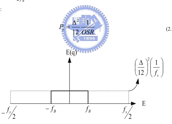
= , as Figure. 2.4, than the quantization power spectral density is reduced to: 2
1
12
eP
OSR
Δ
=
(2.5)2
sf
2
sf
−
−
f
Bf
B⎟⎟
⎠
⎞
⎜⎜
⎝
⎛
⎟
⎠
⎞
⎜
⎝
⎛ Δ
sf
1
12
2Figure 2.4 Quantization noise in an oversampled converter Thus the peak SNR equals to:
(
OSR
)
N
P
P
SNR
e inpeak
10
log
⎟⎟
=
6
.
02
+
1
.
76
+
10
log
⎠
⎞
⎜⎜
⎝
⎛
=
(2.6)9
2.2.2 Noise Shaping
With oversampling technique, the SNR increase 0.5 bit if sampling frequency is doubling. In addition to use oversampling technique to improve the performance of ADCs, we can use noise shaping technique to further increase the SNR of the ADC, by applying a loop filter before the quantizer and introducing the feedback, a
noise-shaping modulator is built and new noise transfer function is realized.
A basic Sigma-Delta modulator is shown in Figure 2.5, it contains a loop filter, a quantizer and a feedback loop. If we assume that the DAC feedback gain is unity, than we can express the output of the SDM is:
Y z
( )
=
STF z X z
( ) ( )
+
NTF z E z
( ) ( )
(2.7)Figure 2.5 A linear model of the sigma-delta modulator
Where STF(z) represents the signal transfer function and NTF(z) represents the noise transfer function. And the STF(z) and NTF(z) can be calculated as:
10
( )
( )
( )
( ) 1
( )
Y z
H z
STF z
X z
H z
=
=
+
(2.8)( )
1
( )
( ) 1
( )
Y z
NTF z
E z
H z
=
=
+
(2.9)With the large gain of H(z) at the frequency band, the STF(z) will approximate unity and the NTF(z) is going to approximate zero over the signal band. Thus the quantization noise is further attenuated than only by oversampling.
2.3 Performance Metrics
The performance metrics is shown at Figure 2.6 with a full scale sine wave to ADC, performed a Discrete Fourier Transform (DFT) to map into Fast Fourier Transform (FFT) spectrum. Some of the performance metrics are listed below, while the unit is “dB”.
1. SFDR: the abbreviation of “spurious free dynamic range”. Difference between the fundamental bin and the highest harmonic bin.
2. SNR: the abbreviation of “signal to noise ratio”. Fundamental power divided by the power of the bins in the FFT other than DC, fundamental and first N harmonic bins.
3. SNDR: the abbreviation of “signal to noise and distortion ratio”. Fundamental power divided by the power of the bins in the FFT other than DC and fundamental bins.
11
4. ENOB: the abbreviation of “effective number of bits”, which is defined at Equation 2.10:
ENOB
=
SNDR
6.02
−
1.76
(
dB
)
(2.10) 5. DR: the abbreviation of “dynamic range”. Effective input range when SNRremains positive. 0 2 4 6 8 10 12 14 x 104 0 20 40 60 80 100 120 140 Frequency [Hz] O ut put s pec tr um [ dB ]
12
Chapter 3
System Considerations
This chapter discusses actual SDM design considerations. We begin with reviewing previous researches then consider power issues in traditional SDM design, and the system parameter considerations are discussed in Section 3.2. Several non-idealities such as gain requirement, settling of OTA and capacitor sizing are discussed in the end of the chapter.
3.1 Power Issues in SDM
There are many researches about how to reduce the power of the sigma-delta modulator for audio band applications in recent years [2-9].
A switched-OPamp technique combined with a dc level shift has been proven to allow proper operation under low VDD conditions (0.7v),thus lower the power consumption[2]; A new fully differential CMOS class AB Operational Amplifier with a charge-pump is proposed [3]; And a load-compensated OTA with rail-to- rail output swing and gain enhancement is used in a 90nm technology [4]; And a 0.6v folded-cascode OTA topology is used in a 2-2 cascade delta-sigma ADC design with a resistor-based sampling technique[5]. A switched-current SDM is used for a bio-acquisition Microsystems with 0.8v power supply. And a Digital Hearing Aid
13
chip is proposed [7]; Then a ADC is designed and optimized for a CMOS image sensor[8]; Finally, a 4th order SDM is presented with a single stage class A OTA and positive feedback[9].
The comparisons of above researches are listed as Table 3.1:
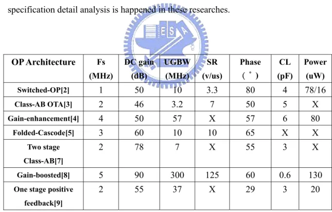
Technology VDD Signal BW(KHz) OSR Peak-SNR (dB) Power JSSC 2002[2] 0.18 0.7 8 64 67 80 ISCAS 2003[3] 0.18 0.9 10 100 74 38 JSSC 2004[4] 0.09 1 20 100 85 140 JSSC 2005[5] 0.35 0.6 24 64 77 1000 TCASI 2006[6] 0.18 0.8 5 64 50 180 JSSC 2006[7] 0.25 0.9 8 128 86 60 IMTC 2007[8] 0.18 1 25 1000 70 150 JSSC 2008[9] 0.13 0.9 20 50 83 60 Table 3.1 Summary of previous SDM papers
Among these researches, a part of them adopt some special analog circuits, such as switched-Opamp technique[2], switch-current topology[6] or resistor-based sampling technique[5] to reduce the power. Moreover, because that the power consumption of a SDM is most consumed at the OTA in loop filter, therefore some of them choose adaptive OTA topology to reduce power [3][4][7][8][9].
14
From above researches, we can observe that the former have a low supply voltage, but generally they often have larger chip area due to the use of extra component. Furthermore, using a low-power OTA in loop filter is an effective method to lower the power consumption of SDM because that the power consumption of a SDM is most consumed at the OTA in loop filter.
There are several specifications we must take care when designing an OTA (such as gain requirement, bandwidth, slew-rate, phase margin, output swing…etc) in Sigma-Delta A/D system conveniently. The specifications of the OTA in these researches are listed at Table 3.2. From the table, we can observe these specifications are followed by the “rule of thumbs” in traditional ADC design mostly. A lack of specification detail analysis is happened in these researches.
OP Architecture Fs (MHz) DC gain (dB) UGBW (MHz) SR (v/us) Phase ( ° ) CL (pF) Power (uW) Switched-OP[2] 1 50 10 3.3 80 4 78/16 Class-AB OTA[3] 2 46 3.2 7 50 5 X Gain-enhancement[4] 4 50 57 X 57 6 80 Folded-Cascode[5] 3 60 10 10 65 X X Two stage Class-AB[7] 2 78 7 X 55 3 X Gain-boosted[8] 5 90 300 125 60 0.6 130
One stage positive feedback[9]
2 55 37 X 29 3 20
Table 3.2 Specification comparison of OTA
In fact, traditional design rules are not optimized according to low-power concern, so specifications optimization is needed in low-power demand SDM design. Therefore, we try to use a suitable OTA topology, and then we optimize the power
15
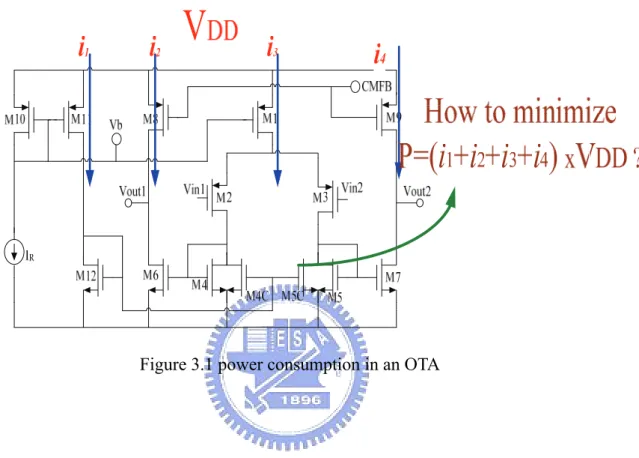
consumption by minimizing the total current consumption of OTA such as Figure 3.1 shows in this thesis. No special technology or extra analog devices is needed, thus the chip area and cost are also lower compared to previous researches.
Figure 3.1 power consumption in an OTA
3.2 System Parameter Considerations
Our design goal is to achieve a lowest power consumption SDM while the target SNR (DR) is high enough for audio band portable electric devices applications. There are many trade-offs when designing a low-power SDM, thus three steps are followed in this section to determine the system parameters of the SDM, topology decision, architecture selection and coefficient decision, respectively.
16
3.2.1 Topology Decision
The first step to design a sigma-delta modulator is to determine the system level parameters based on the modulator specifications while the power consumption can be minimized. The power consumption formula:
(
)
2
Power
= × = × ×
I V
f c
Vdd
(3.1)Therefore, we must choose the supply voltage we used in this thesis. The basic principle is to reduce power, and in TSMC 0.18um technology, vtn+vtp~0.9v, so we choose supply voltage is one volt for some design.
The system-level parameters include oversampling ratio (OSR), the loop filter order (L), the number of the quantizer level (N).
First we decide N. Because the power consumption of the quantizer increases proportionally with N, and a multi-bit quantizer have more complicated DAC structure, thus will make whole circuit more complicated and consume more power, so for a low-power SDM design, the number of the quantizer should be minimized, so we choose N=1.
Second, because single-stage structure has more advantages on low-power design, for example simple analog circuit, good circuit mismatch characteristic, so single stage architecture is selected.
Therefore, for a target SNR, the oversampling ratio (OSR) can be made after deciding the loop filter order n:
17
(
)
2 13
10 log
2
1
2
n in peak eP
OSR
SNR
n
P
π
π
+⎛
⎞
⎛
⎞
=
⎜
⎟
=
+
⎜
⎟
⎝
⎠
⎝
⎠
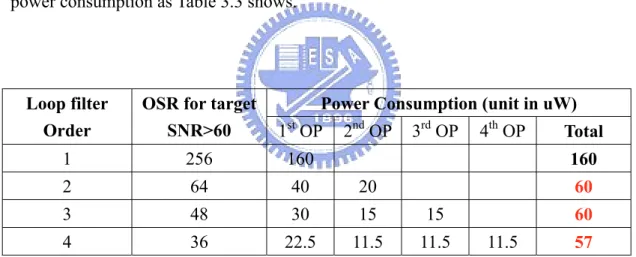
(3.2)A higher loop filler order n have more switches and integrators, lower sampling frequency, and higher order of n has more stability issue. So we have to make a trade-off between the order and the sampling frequency. If we compare different order N by simple estimation (suppose power consumption is proportional to sampling frequency), we can know that for loop filter order 2, 3, and 4, we can have similar power consumption as Table 3.3 shows.
Power Consumption (unit in uW) Loop filter
Order
OSR for target
SNR>60 1st OP 2nd OP 3rd OP 4th OP Total
1 256 160 160
2 64 40 20 60
3 48 30 15 15 60
4 36 22.5 11.5 11.5 11.5 57
Table 3.3 Power comparison of different loop filter order
Therefore, a second order architecture, 1-bit with OSR=64 is chosen because of the simplicity of the analog circuits, thus we can use simpler circuit to achieve the same target SNR.
18
3.2.2 Architecture Selection
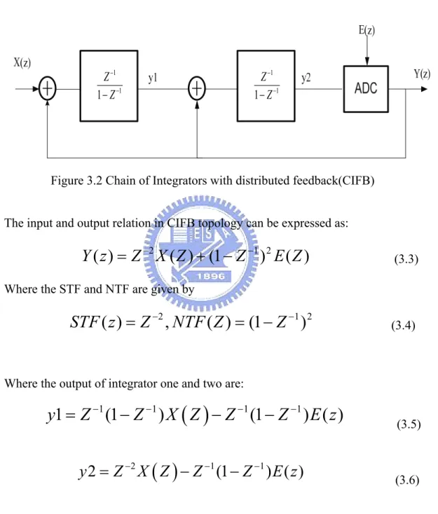
The most general single stage topology in the SDM design is the CIFB architecture, and it is shown at Figure 3.2:
1 1 1 − − − Z Z 1 1 1 − − − Z Z
Figure 3.2 Chain of Integrators with distributed feedback(CIFB) The input and output relation in CIFB topology can be expressed as:
Y z
( )
=
Z X Z
−2( ) (1
+ −
Z
−1 2)
E Z
( )
(3.3) Where the STF and NTF are given by2 1 2
( )
,
( ) (1
)
STF z
=
Z
−NTF Z
= −
Z
− (3.4)Where the output of integrator one and two are:
( )
1 1 1 11
(1
)
(1
) ( )
y
=
Z
−−
Z
−X Z
−
Z
−−
Z
−E z
(3.5)( )
2 1 12
(1
) ( )
y
=
Z X Z
−−
Z
−−
Z
−E z
(3.6)From the equations, we can know that the output signal of the integrators are the functions of input signal x(z), so if we want to have a full scale input signal x(z), than there will be a large output swing at y1(z) and y2(z),hence the power of the OPAMP will increased .
19
If the x(z) has a smaller input signal, than the target SNR of the modulator will be degraded. So this feature make the CIFB topology have some restriction for low-power design.
Because the nature restriction of the CIFB architecture, another architecture is chosen for low-power design [1], the CIFF architecture have some advantages, and its figure is shown at Figure 3.3:
1 1 1 − − − Z Z 1 1 1 − − − Z Z
Figure 3.3 Chain of integrators with weighted feed-forward summation. (CIFF)
The input and output relation in CIFF topology can be expressed as:
)
(
)
1
(
)
(
)
(
z
Z
2X
Z
Z
1 2E
Z
Y
=
−+
−
− (3.7)Where the STF and NTF are given by:
2 1
)
1
(
)
(
,
1
)
(
z
=
NTF
Z
=
−
Z
−STF
(3.8)Where the output of integrator one and two are:
( )
Z
E
Z
Z
y
1
=
−
−1(
1
−
−1)
(3.9)( )
Z
E
Z
y
2
=
−2 (3.10)20
From above equations, we observed that the output signals of two integrators y1 and y2 in CIFF structure are not contain the input signal x(z),which means that this loop filter process E(z) only, thus the output swing requirements of the loop filter will decrease ,it means that the slew-rate requirement is not critical when we design the OPAMPs in loop filter[3], so it is more suitable for low-power applications.
3.2.3 Coefficient Decision
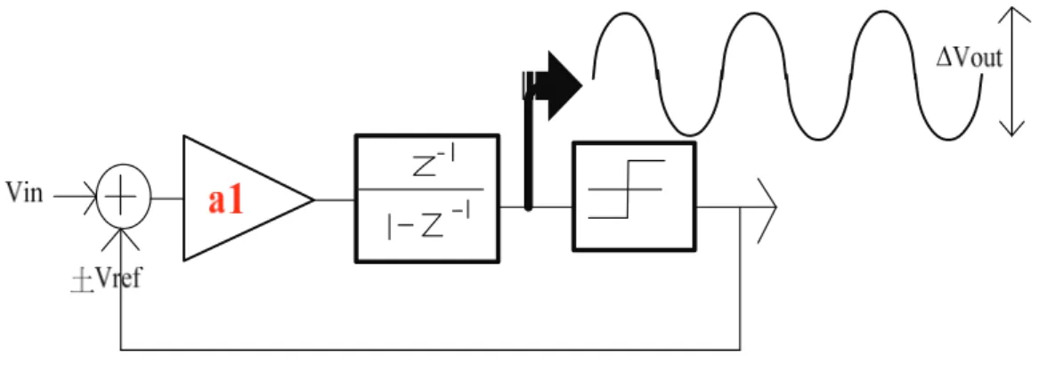
In a general structure of CIFF sigma-delta modulator like Figure 3.4, the modulator contains five coefficients: two integrator gain (a1, a2) and three summation factor (b0, b1, b2):
Figure 3.4 Simulink model of a 2nd-order CIFF SDM
From the Delta-Sigma Toolbox, give order=2, OSR=64, the noise transfer function (NTF) that have SNR(max):
(
)
4415 . 0 225 . 1 1 ) ( 2 2 + − − = z z z Z NTF (3.11)21
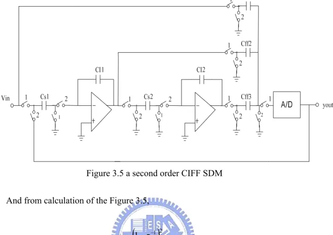
Figure 3.5 a second order CIFF SDM And from calculation of the Figure 3.5,
(
)
2 1 2 1 ) 1 1 1 2 2 1 ( ) 2 1 1 ( 1 1 − − − + − + − + − + = z b a b a a z b a z x y (3.12)Therefore,
a
1
b
1
=
0
.
775
anda
1
a
2
b
2
=
0
.
2165
must be met.After deciding the transfer function of the SDM, we must decide which combination of (a1, a2, b1, b2, b3) we will use. Because our design target is to achieve low-power, and the most important feature of a low power SDM is that the signal swing at the loop filter output must be small.
22
Figure 3.6 A general linear model of SDM
Figure 3.6 is a general case first-order SDM, we can know that when the coefficient a1 is larger, the output swing of the loop filter is larger ,then the power consumption is larger of the whole modulator; therefore, if we want to have a smaller signal swing, the a1 coefficient must be minimized.
However, if a1 is too small, the stability of the SDM will be degraded because the signal will overload, and the SNR will decrease, so we must make a trade-off between the coefficients.
In this work, we choose a1=0.25 and b1=3,combined above requirement, capacitor matching and the signal scaling issues, the coefficients of the second-order modulator is listed at Table 3.4:
Integrator Coefficients Feed-Forward Coefficients
a1=0.25 b0=1
a2=1 b1=3 b2=1
23
Under the coefficients, the modified NTF becomes:
(
)
5 . 0 25 . 1 1 ) ( 2 2 ' + − − = z z z Z NTF (3.13)It cause a slightly change of the NTF pole and it will not degrade the SNR significantly.
The ideal Output spectrum of 8192-point FFT with 8k input signal is shown at Figure 3.7, the simulation result reveals that the SFDR exceed 78dB.
24
3.3 Non-idealities Considerations
The above simulations show an ideal model of the second-order sigma-delta modulator. However, there are some non-ideal effects in analog circuit design and it is unavoidable, so we must evaluate the non-ideal effect to make our designs meet the desired margin.
3.3.1 Gain requirement
The transfer function of an ideal integrator:
1 1 1 ) ( − − − = Z Z z H (3.14)
However, the gain of OTA cannot be infinite in circuit design, when a finite gain is A in an OTA, the transfer function will become:
1 1 ) 1 ( 1 ) ( − − − − = Z Z z H ε (3.15) Where I S C C A⋅ = 1 ε
25
A finite gain of OTA means that the pole of the H(Z) will depart from unit circle, and when the distance of the zero exceed about
1 1 S I C C OSR⋅ π
, the noise attenuation of NTF begins to degrade, so the lower limit of A is about 40 dB[10].
3.3.2 Settling of the OTA
In a switched-capacitance circuit, the loop filter can be separately into two parts, namely the sampling period and the integration period, as shown at Figure 3.9:
Figure 3.9 Sampling and integration period of a loop filter
When the loop filter is at integration period, the settling behavior of the OTA can be derived as the Figure 3.10. A slewing is happened when a large output change of the loop filter. When the differential input voltage is less than 2VOV, the OTA enters
linear settling region. Because of the speed limitation of the OTA, settling error will occur at the end of integration period as the Figure 3.10 shown, so we must take settling error into consideration when designing OTA.
26
s
Rlinear
∆Vout
Settling error OVV
2
Figure 3.10 Settling behavior of OTA
3.3.3 Capacitor Sizing
The input-referred thermal noise of the integrator is:
s n C KT V 2 = , (3.16) Where Cs is sampling capacitor of the integrator.
With an oversampling ratio of OSR, the in-band KT/C noise:
(
OSR)
C KT V s n = ⋅ 2 ' (3.17)And if for a full scale input amplitude, the in-band noise power must be at least 85dB below the signal power:
2 1 2 10 2 5 . 8 2 ' ⋅ ⎟ ⎠ ⎞ ⎜ ⎝ ⎛ ⋅ ≤ − DD n V V (3.18)
27 Ö
(
OSR)
V peak SNR KT C DD S ⋅ ⋅ >8 (2 _ ) (3.19)Ö It can be calculated that Cs> 0.163pF
The simulation result of first sapling capacitor is shown at Figure 3.11, from the figure we choose Cs1=0.5pF for safety noise margin.
Figure 3.11 Simulation result of the first sampling capacitor
The KT/C noise at the input of the second integrator is shaped by the first-order noise shaping, so that Cs2 can be scaled down since its effect of thermal noise is fewer. In this SDM system, we choose CS2=0.2pF.
28
Chapter 4
Circuit Implementation
The proposed sigma-delta modulator has been fabricated in TSMC 0.18um single-poly six-metal CMOS process. The circuitry is operating at a supply voltage of 1 volt. The sub-blocks which including OTA, comparator, clock generator and switched capacitor circuit in SDM are described in Section 4.1. In Section 4.2, the simulation results of sub-blocks and whole SDM are presented. In Section 4.3, the final layout design of proposed SDM is then described.
4.1 Transistor Level Design
After considering the system parameters and non-idealities of proposed SDM, the following is the circuit implementation. The sub-circuit of each component in this modulator is presented including OTA, 1-bit quantizer, clock generator, switched capacitor circuit, respectively.
4.1.1 Differential OTA in loop filter
The OTA in loop filter is the analog block which consumes the most power, and it also dominant the performance of the modulator, so it is the most critical building block that we must design it seriously.
29
In previous researches, a single stage OTA must used because it doesn’t have to waste extra current in driving the compensated capacitance[4], and although the class-AB OTA is the most widely used OTA architecture when designing a low power SDM, it requires extra paths to drive the transistor of output stage[9]; Therefore, a single-stage class-A Amplifier with positive feedback to increase its gain is used in this design, as shown in Figure 4.1, We use PMOS as the input transistor because of two reasons:
(1)The input common mode voltage (ICM) is low than Vt
(2)The noise of PMOS input pair is smaller than NMOS
Figure 4.1 Single Stage Class-A OTA with positive feedback
An OTA in loop filter works at the integration period, and the settling behavior of the OTA can be divided into two parts, the slewing and the settling time. A slewing is happened when a large output change of the loop filter. When the differential input voltage is less than 2VOV, the OTA enters linear settling region, with a 2MHz clock,
30
ns
T
T
SR+
settling=
250
(4.1)A trade-off between the slewing time and linear settling time means different settling behavior of the OTA. The proposed optimization technique is to find the optimization of slewing-settling trade-off as shown in Figure 4.2, thus the total current consumption of the OTA can be minimized, and the analysis is followed.
OV
V
2
Figure 4.2 trade-off between slewing and linear settling
The slewing behavior is related to the current of output path:
SR load out T V C I = ⋅Δ 2 (4.2)
For a load capacitance of 2.5pf and a v=0.5, we can derive that: SR out T x I 13 10 49 . 4 − = (4.3)
31
The speed of the OTA settling is depend on its time constant, therefore , the unit gain bandwidth, therefore the input path current of the OTA, we set the linear settling period is larger than 10 time constant , thus the settling error is lower than 85dB.
Therefore,
T
linear≥
10
τ
(4.4)So, the unit-gain bandwidth:
linear T GBW 1.59 21 = = πτ (4.5)
And, = π −α 1 2 1 B C g GBW L m
for the input of the OTA,
Î
t GS in load m V V I B C GBW g − = − ⋅ ⋅ = 2 1 2 1 α π (4.6)Î
(
)
B C V V T I GS t load t linear in α π⋅ − − = 1.59 2 1 (4.7)For VOV =0.1v,α =0.25,B=4, we can derive that:
linear in T x I 13 10 78 . 0 − = (4.8)
From (3.16) and (3.21) we can know that the total current consumption of the OTA:
(
)
SR SR linear SR out in total T x T x T x T x I I I − + = + = + = − − − − 250 10 56 . 1 10 98 . 8 10 56 . 1 10 98 . 8 2 13 13 13 13 (4.9)32
Therefore, we can optimize the OTA to minimize the total current consumption of the OTA by plotting it as a function of the slewing time such as Figure 4.3:
Figure 4.3 Slewing time versus total current of the OTA
From this figure, we know that the minimum current occurs at TSR=160~170ns.
However, when TSR=170 ns is used, and we can calculate that: uA T x I linear in 1.3 10 78 . 0 13 = = − (4.10) I Tx uA SR out 2.56 10 49 . 4 13 = = − (4.11)
Then the coefficient B of the OTA is about 3, which departs from our assumption, so we must decrease the TSR so that the B is close to 4, we modify the
slewing time so that TSR=130ns as Figure 4.4 plots, therefore: uA T x I SR out 3.45 10 49 . 4 13 = = − (4.12)
33
Figure 4.4 modification of the slewing time
Therefore, the current consumption of our calculation can be simplified as Figure 4.5:
34
The transistor size summary of the first OTA is shown at Table 4.1:
Transistor W L M M1,2 1 0.8 4 M3,4 0.6 0.8 1 M5,6 0.48 0.8 1 M7,8 0.6 0.8 4 M9,10 4.16 1.5 1 M11,12 4.16 1.5 3 M13 2 1.5 8 Table 4.1 Device ratio summary of first OTA
The decision of the size is based on the following principles:
(1) Tune M13 that the current of M13 as we want and the overdrive voltage= 100mv. (2) Tune M1, M2 to meet the gm and Fu specification.
(3) Tune M3~M6 to adjust the second pole, and the positive feedback gain is 0.8 at the same time.
(4) Tune M7, M8 to meet the assumption that B=4 we used above.
(5) Tune M9~12 that the output stage has a output closed to 0.5Vdd, and the gain of the whole OP exceed 50dB.
A larger length of the transistor is used (0.8um) is because that the overdrive voltage, low current and corner consideration. In order to achieve a low-power and stable OTA, some area is trade for our requirement.
The design procedure of the second stage OTA is similar to the first one, except that B=4 we used in first OTA is adjust to B=2 in second stage due to the parasitic capacitance at the output of this OTA is smaller than the first OTA, thus the power consumption can be lowered as Figure 4.6 is shown:
35
Figure 4.6 Current consumption of second OTA
The performance summary of the first OTA is listed at Table 4.2:
Specification Result Gain 61.9dB
Unit Gain Bandwidth 22.2MHz
Phase Margin 37°
Slew Rate 3.8 v/us
Settling Time Constant 12ns
Output Swing 800mv
Power Dissipation 10.14uW
Table 4.2 Summary of first OTA simulation results
The comparison of the two OTA for a 2.5pf loading capacitance is listed at Table 4.3, and the frequency response of the first OTA is shown at Figure 4.7:
Gain(dB) GBW Total Power
OTA1 61.9dB 22.2MHz 10.14uW
OTA2 61.6dB 15.1MHz 6.67uW
36
Figure 4.7 Frequency Response of first OTA
The comparison of the OTA before and after this current optimization technique is listed at Table 4.4. It shows that the total current consumption is form 14.5uA to 10.2 uA. It means at least 30.1% current reduction in OTA.
OP Architecture Fs (MHz) UGBW (MHz) SR (v/us)
Iin Iout Power
(uW)
Switched-OP[2] 1 10 3.3 78/16
Gain-enhancement[4] 4 57 X 80
One stage positive feedback[9]
2 37 X 20
Traditional specification
(the same architecture)
10 7 0.8 6.45 14.5
Proposed optimize method
2
22 3.8 1.6 3.5 10.14
Table 4.4 Comparison before/after current optimization
Because of the differential architecture of the OTA, so we must have a CMFB circuit, thus a dynamic CMFB circuit like Figure 4.8 is used because it is the most power-efficient. In the CMFB circuit, Vcmo is set to 0.5v and only the switch connect to CMFB use CMOS switch, other switches is PMOS switch only.
37
Figure 4.8 Dynamic CMFB circuit
The device ratio summary we used in CMFB circuit is listed at Table 4.4, and the transient response of the first OTA and CMFB circuit is shown below at Figure 4.9:
Transistor Type W/L Transistor Type W/L
PMOS 2/0.6 NMOS 1/0.3 Capacitor Value Capacitor Value
C1 0.1pf C2 0.4pf Table 4.5 CMFB circuit summary
38
4.1.2 1-bit Quantizer
The 1-bit quantizer is realized with a comparator and a SR latch, shown at Figure 4.10. The comparator is a dynamic comparator to lower average power consumption, when CLK is high, the comparator compares the two input voltage, then the comparison result is followed by the SR latch behind the comparator.
Figure 4.10 a power-efficient 1-bit quantizer
The simulation result of the 1-bit quantizer is shown at Figure 4.11, for a 16KHz input signal and a clock of 4MHz, the quantizer compare the input signal correctly. After the simulation result, the device ratio of the quantizer is listed at Table 4.6.
39 Width(um) Length(um) M M1a,b 2.5 0.5 2 M2a,b~M5a,b 0.5 0.18 1 M6a,b 0.5 0.18 5 M7a,b 0.5 0.18 1 M8a,b 0.5 0.18 5 M9a,b 0.5 0.18 1
Table 4.6 Quantizer transistor size summary
4.1.3 Clock Generator
The on-chip clock generator is shown as Figure 4.12, an external clock input signal is buffered and then two non-overlapping clock phases are generated. To avoid the signal dependent charge injection, two delayed clocks, i.e., C1d and C2d, are also be generated.
40
The output of the clock generator are four different clock phases, the simulation results are shown at Figure 4.13, and Figure 4.14 shows that the phase one and two are non-overlapped each other.
Figure 4.13 Output of the clock generator
41
4.1.4 Switches
The current of a MOS switch:
(
GS DS)
DS ox n DV
V
V
L
W
C
u
I
=
−
(4.13) Therefore, the turn-on resistance of the NMOS, PMOS and CMOS switches can be derived as:)
(
1
in tn DD OX n NMOSV
V
V
L
W
C
u
R
−
−
=
(4.14))
(
1
SS tp in OX n PMOSV
V
V
L
W
C
u
R
−
−
=
(4.15))
(
1
//
)
(
1
SS tp in OX n in tn DD OX n CMOSV
V
V
L
W
C
u
V
V
V
L
W
C
u
R
−
−
−
−
=
(4.16) It is clearly that:(1) Use NMOS switch as much as we can due to the area consideration. (2) When the input signal of the MOS switch is large, us CMOS switch.
(3) Large ratio of W/L can lower the turn-on resistance of the switches, but have larger area and parasitic capacitance.
42
4.2 Modulator Design and Simulation
A second-order sigma-delta modulator with CIFF topology is done as Figure 4.15:
Figure 4.15 2nd order CIFF SDM
The Sigma-Delta modulator is implemented by fully differential input and output signal, the building blocks in this figure are done as we described in previous sections. With a 8k input signal and a -6dB full scale input amplitude, the simulated time-domain integrator output signal and the frequency-domain output spectrum can be observed by Figure 4.16 and Figure 4.17, respectively:
43
Figure 4.16 output signal of input and two integrator outputs
44
The FFT shows that the SNR=69.1, SNDR=68.4 and the SFDR=77.2dB, and the dynamic range (DR) is about 72dB as Figure 4.17 and Figure 4.18 shows.
Figure 4.18 Dynamic range of the SDM
Beside this, because of the possibly process variation, we simulate the SNR results of four corners, the corner simulation results are summarized at Table 4.7.
Unit(dB) TT FF SS SF FS
SNR 69.1 60.2 63.0 58.6 61.2
SNDR 68.4 56.9 61.1 56.6 60.3
45
4.3 Layout Level Design
A physical design in the context of integrated circuit is referred to as layout. Effects of parasitic components and mismatching will damage the performance of the chip, so layouts must be considered heavily in design process. Several principles of layout must be obeyed to minimize cross-talk, mismatches include (a) multi-finger transistors (b) symmetry (c) dummy cell (d) common centroid.
The diagram of layouts are shown at Figure 4.20, there are twenty-two I/O pads, including a pair of differential inputs, a pair of modulator outputs, a input clock, five reference voltages and eleven VDD/GND lines. The I/O pad description is listed at Table 4.7. This circuit is fabricated in a 0.18um 1P6M 1.8V standard CMOS technology with MIM process. The chip area is 0.665mm including ESD-protection 2
I/O pads and 0.05mm for the core area. 2
46
The proposed chip is fabricated in a 0.18um 1P6M 1.8V standard CMOS technology with MIM process. And the package type is S/B type 24 pin, as shown in Figure 4.21 where the actual chip photograph is shown at Figure 4.22. The pin assignment is listed at Table 4.8.
Figure 4.20 Diagram of the 24 pin DIP package
47
Pin Name Description
1 AGND Analog circuit ground
2 vrefn Reference voltage
3 NC No connection
4 vrefp Reference voltage
5 AGNDPAD ESD PAD ground
6 DGNDPAD ESD PAD ground
7 DGRGND Digital circuit guard ring
8 Ck_out input clock signal
9 Ck Clock signal output
10 NC No connection
11 DGND Digital circuit ground
12 DVDD Digital circuit VDD
13 Vo2 Differentail output signal
14 Vo1 Differentail output signal
15 DVDDPAD ESD PAD Digital VDD
16 AVDDPAD ESD PAD Analog VDD
17 AGRVDD Analog circuit guard ring 18 AGRGND Analog circuit guard ring
19 Vcmo Reference voltage
20 Vcmi Reference voltage
21 vb Reference voltage
22 AVDD Analog circuit VDD
23 Vin1 Differential input signal
24 Vin2 Differential input signal
Table 4.8 Pin Assignments
The 8192-point FFT of the post simulation result is shown as Figure 4.23 with an input frequency of 4k and the input amplitude is -6dB of full scale. This spectrum shows the SNR is 63.4dB while the SNDR is 58.7dB, and the comparison of pre-simulation and post-simulation is listed at Table 4.9.
48 102 103 104 105 106 107 30 40 50 60 70 80 90 100 110 120 Frequency [Hz] O ut put s pe ct rum [ dB]
Figure 4.22 8192-point FFT of the post-simulation result
Unit(dB) Pre-Simulation Post-Simulation
SNR 69.1 63.4 SNDR 68.4 58.7
Table 4.9 Comparisons of pre & post simulation
Finally, the performance summary of the proposed SDM is listed at Table 4.10, the simulation result shows that the peak SNR is 63.4dB for a 16 KHz signal bandwidth and sampling frequency of 2MHz. With a 0.18um technology, the average power consumption is only 18uW.
Technology 0.18um VDD 1V
Signal Bandwidth 16KHz
Sampling Frequency 2MHz
Peak SNR 63.4dB
Power Consumption 18uW
Layout Core Area Size 240um x 210um
49
4.4 Comparison
The comparison of this work and previous researches are listed at Table 4.11 and Figure 4.24, in order to compare the design result, we define the figure-of-merit as:
⎟
⎠
⎞
⎜
⎝
⎛
+
=
P
BW
SNR
FOM
dB10
log
Tech VDD Signal BW(KHz) OSR PeakSNR (dB) Active Area (mm^2) Power FOM JSSC 2002[2] 0.18 0.7 8 64 67 0.082 80 147 ISCAS 2003[3] 0.18 0.9 10 100 74 0.27 38 158 JSSC 2005[5] 0.35 0.6 24 64 77 2.88 1000 151 TCASI 2006[6] 0.18 0.8 5 64 50 0.05 180 124 IMTC 2007[8] 0.18 1 25 1000 70 150 136 pre-layout simulation 69.1 16.1 159.1 post-layout simulation 0.18 1 16 64 63.4 0.0504 18 152.9Table 4.11 Comparison of this work
50
The FOM comparison shows that the power consumption of proposed SDM is lowest compared to other researches while the FOM is still above average. The SNR versus power comparison is shown at Figure 4.24.
Performance Comparison 0 20 40 60 80 100 120 140 160 180 200 40 50 60 70 80 90 SNR Po w er [This work(po-sim)] [This work(pre-sim)] [6] [8] [2] [7] [9] [4] [3]
51
Chapter 5
Testing Setup and Measurement
A testing setup for fabricated chip is presented in this chapter. And a costumed designed printed circuit board (PCB) is designed and fabricated to integrate the targeting prototype chip in order to measure the performance metrics of proposed design. Following by the setup for measurement, the experimental results is presented and discussed. And the performance summary is summarized in the end of this chapter.
5.1 Testing Environment Setup
The testing environment setup is shown as Figure 5.1. It includes a printed circuit board (PCB) including a device under test (DUT) board, a logic analyzer (Agilent 16902A), an audio signal generator (Stanford Research DS360), a power supply (E3610A), a mixed-signal oscilloscope (Agilent 54641D) and a PC to analyze the output bit stream of proposed modulator.
52
Figure5.1 experimental test chip
As shown in Figure 5.1, the input signal is generated by audio signal generator, and the digit output is fed to the logic analyzer, then load to PC for MATLAB simulation. A PCB board combines the clock generator (a crystal oscillator) and a device under test (DUT) to measure the chip. The photograph of the measurement environment is shown at Figure 5.2.
53
5.2 Measurement Result
The measurement result of proposed chip is failed. The probably reason is that the transistor size of the output buffer is too small to push the ESD PAD and the parasitic capacitance of the packages as Figure 5.3 shows.
Figure 5.3 Probably problem of output buffers
Stage1 Stage
2
1um/0.18um 4um/0.18um
Table 5.1 Output buffer device ratio summary
Due to the problem of this layout, we modify the design as Figure 5.4, and it is modified by following principles:
1. ESD protection for analog input signals while the output pad is pure pad to reduce chip area and measuring core power of proposed SDM.
2. Wider metal for power lines.
3. Independent PAD for different supply voltage: AVDD, DVDD, IOVDD to measure the power respectively.
54
Stage 1 Stage 2 Stage 3 Stage 4 Stage 5 Stage 6
1/0.18um 3/0.18um 9/0.18um 27/0.18um 81/0.18um 243/0.18um Table 5.2 the modified output buffer device ratio summary
Figure 5.4 modified version of layout
We also take the measurement of the core power into considerations of the modified version of layout, we use three independent supply voltage pads for analog circuits (part A), clock generator circuit (part B) and output buffer (part C), respectively. The
55
simulation results of the power consumption for three parts are listed at Table 5.3, and the post layout simulation results are shown at Figure 5.5. The simulated result of SNR and SNDR are listed at Table 5.4.
A A+B A+B+C
Power(uW) 14.3 18.0 25.4
Table 5.3 Power consumption for three parts circuits
Figure 5.5 8192-point FFT of the modified layout
Unit(dB) Pre-Simulation Post-Simulation Modified layout
SNR 69.1 63.4 61.3
SNDR 68.4 58.7 57.9
56
5.3 Summary
The circuit present in this thesis is implemented by design considerations described in Chapter 3 and circuit design implementation in Chapter 4.This work emphasized the complete design flow for low-power design and the current optimization of the OTA by discussing the slewing-settling trade-off of it.
The predicted resolution of the SDM is 11.2 bits (68.4dB), and the post-simulation result is 9.6 bits (58.7dB). It can be used in the audio electrical portable devices applications.
57
Chapter 6
Conclusions
This thesis describes the design and implementation of a low-power second-order sigma-delta modulator (SDM) with CIFF structure for audio-band applications. A single stage class-A positive feedback OTA with current optimization has been presented to lower the power of SDM.
Using 0.18um CMOS technology, this modulator achieves SNR of 63.4dB with 16KHz bandwidth. With a moderate target signal-noise-ratio (SNR), it is suitable for battery-based operation system, such as mp3 players, biomedical electronic and digital hearing aid instrument applications. The simulation results show that the power consumption is 18uW. It is the lowest compared to references [2]-[9].
The future work is to integrate the modified version from the problems of proposed SDM. A low-power measurement consideration is included in the modified SDM design consideration.
After this modified layout, a high resolution sigma-delta modulator can be done using the same method of optimizing the power of the OTA.
58
References
[1] J.Silva, U.Moon, J.Steensgaard and G.C.Temes,” Wideband low-distortion delta-sigma ADC topology,” Electronics Letters, Vol. 37, pp.737-738, June 2001. [2] J.Sauerbrey, T.Tille, D. Schmitt-Landsiedel, R.Thewes, ”A 0.7V MOSFET-Only Switched-Opamp Modulator in Standard Digital CMOS Technology”, IEEE Journal of Solid-State Circuits,” Vol. 37, No. 12, Dec 2002.
[3] Yamu Hu; Zhijun Lu; Sawan, M., “A low-voltage 38μW sigma-delta modulator dedicated to wireless signal recording applications,” Circuits and Systems, ISCAS 03, vol.1, pp.1073-1076, May 2003
[4] L.Yao, Michael S.J.Steyaert, W.Sansen, “A 1v 140uW 88dB Audio Sigma-Delta Modulator in 90nm CMOS,” IEEE Journal of Solid-State Circuits, Vol. 39, No. 11, Nov 2004.
[5] G.Ahn, M.E.Brown , N.Ozaki, H.Yiura, K.Yamamura, K.Hamashita, K.Takasuka, G.C.Temes, “A 0.6V 82dB Delta-Sigma Audio ADC Usgin Switched-RC Integrators,” IEEE Journal of Solid-State Circuits, Vol.40 , No. 12, Dec 2005. [6] S.Lee, C.Cheng, “A Low-Voltage and Low-Power Adaptive Switched Current
Sigma-Delta ADC for Bio-Acquisition Microsystems,” IEEE Transactions on Circuits and Systems-Regular Papers, Vol. 53, No.12, Dec 2006.
[7] S.Kim, J.Lee, S.Song, H.Yoo, “An Energy-Efficient Analog Front-End Circuit for a Sub-1V Digital Hearing Aid Chip,” IEEE Journal of Solid-State Circuits, Vol.41 , No.4 , Apr 2006.
[8] Mahmoodi, A.; Joseph, D, “Optimization of Delta-Sigma ADC for Column-Level Data Conversion in CMOS Image Sensors,” IMATC 2007, pp. 1-6, May 2007.
59
[9] J. Roh, S.Byun, Y.Choi, H.Roh, Y.Kim, J.Kwon, “A 0.9V 60uW 1 bit Fourth-Order Delta-Sigma Modulator with 83dB Dynamic Range,” IEEE Journal of Solid-State Circuits, Vol.43, No.2, Feb 2008.
[10] Richard Schreier, G.C Temes, ”Understanding Delta-Sigma Data Converters,” Institute of Electrical and Electronics Engineers Inc, 2005.
[11] Shahiar Rabii , Bruce A.Wooley,” The Design of Low-Voltage , Low-Power Sigma-Delta Modulators,” Kluwer Academic Publishers 1999.
[12] Roubik Gregorian, ”Introduction to CMOS OP-AMPS and Comparators,” John Wiley & Sons, 1999.
[13] Libin Yao; Steyaert, M.; Sansen, “0.8-V, 8-μW, CMOS OTA with 50-dB gain and 1.2-MHz GBW in 18-pF load,” Solid-State Circuits Conference, pp.297-300, Sep. 2003.
[14] Taha, I.Y.; Ahmadi, M.; Miller, W.C,”A sigma-delta modulator for digital hearing instruments using 0.18μm CMOS technology,”System-oon-Chip for Real-Time Applications, pp.233-2369, July 2004.
[15] Yavari, M.; Shoaei, O.; Afzali-Kusha, ”A very low-voltage, low-power and high resolution sigma-delta modulator for digital audio in 0.25-μm CMOS,” Circuits and Systems,2003. ISCAS, vol. 1, pp. 1045-1048, May 2003.
[16] Carrillo, J.M.; Montecelo, M.A.; Neubauer, H.; Hauer, H.; Duque-Carrillo, J.F, ”1.8-V second-order ΣΔ modulator in 0.18-μm CMOS technology,” Circuit Theory and Design, vol. 1, pp. 197-200, Sept 2005.
[17] Ranjbar, M.; Lahiji, G.R.; Oliaei, O, “A low power third order delta-sigma modulator for digital audio applications,” Circuits and Systems, ISCAS, pp.4762, 2006.
60
[18] Tsung-Hsien Lin; Chin-Kung Wu; Ming-Chung Tsai, “A 0.8-V 0.25-mW Current-Mirror OTA With 160-MHz GBW in 0.18-μm CMOS,” Circuits and Systems, IEEE Transactions on, Vol. 54, pp. 131-135, Feb 2007.
[19] Suarez, G.; Jimenez, M.; Fernandez, F.O, “Behavioral Modeling Methods for Switched-Capacitor Σ∆ Modulators,” Circuits and Systems, IEEE Transactions on, Vol. 54, pp. 1236-1244, June 2007.
[20] Marques, A.; Peluso, V.; Steyaert, M.S.; Sansen, W.M, “Optimal parameters for ΔΣ modulator topologies,” Circuits and Systems, IEEE Transactions on, Vol. 45, pp. 1232-1241, Sep 1998.