JO U R N A L O F M A T E R IA L S S C I E N C E : M A T E R I A L S I N E L E C T R O N I C S 8 ( 19 9 7 ) 31 3 — 3 2 0
Structural and electrical properties of cerium
dioxide films grown by RF
magnetron sputtering
W E N - C H O U T S AI , T S E U N G - Y U E N T S E N G
Institute of Electronics and Department of Electronics Engineering,
National Chiao-Tung University, Hsinchu, Taiwan
A systematic study was performed on the structural and electrical properties of cerium dioxide thin films grown on Si substrate with various deposition temperatures by RF magnetron sputtering. The films grown at 200 °C are partly amorphous whereas those grown above 250 °C are polycrystalline. An amorphous layer of SiO2 forms at the interface between the cerium dioxide film and the Si substrate. Cerium dioxide film grown at higher temperatures up to 500 °C sustains more leakage current on the basis of current—voltage measurements. The electrical conduction of the films is well fitted by a power-law relation, which is explained as space-charge-limited current conduction with exponential distributed traps in the band gap. The variations of dielectric constant, flatband voltage, fixed oxide charge and interface-trapped charge with deposition temperature were studied by making capacitance—voltage measurements on an Al/CeO2/Si structure. The variations of electrical properties with temperature are strongly correlated with the formation of an amorphous SiO2 layer.
1. Introduction
Cerium dioxide has long been used in optical coating and polishing due to its transparency, chemical stabil-ity and hardness [1—3]. It shows an ionic conduction mechanism in its non-stoichiometric form and has attracted much investigation for use in gas sensors [4—7]. Due to its lattice match with high temperature superconductors, cerium dioxide has been widely adopted as the material of buffer layers or insulating layers for the growth of single-layer or multilayer epitaxial high temperature superconductor thin films [8—10]. It has also attracted renewed interest because of its potential application as a capacitor dielectric in dynamic random access memories (DRAMs) due to its relatively high dielectric constant of 26, compared with 3.9 for silicon dioxide [11—13].
We have explored the structural properties of epi-taxial CeO2 thin film grown on MgO and sapphire substrates [14]. However, the substrates are insulators and the electrical conduction is therefore limited. This study examines the structural and electrical properties of CeO2 thin films grown on silicon substrates by RF magnetron sputtering.
2. Experimental procedure
CeO2 thin films were deposited on p-type (1 1 1) sili-con wafers with resistivity 4—7) cm using RF magnet-ron sputtering in an argon plasma. The magnets of the sputter gun were arranged in an unbalanced figure with a weaker central magnet [15]. Compared with
a balanced configuration, this magnet assembly ap-pears to produce a smoother film surface and a higher deposition rate at low pressures. Details of the depo-sition setup are reported in the literature [14]. The target was a sintered CeO2 disc of diameter 2in. (51 mm). Before deposition the wafer was cleaned in aqueous H2SO4 to remove organic and metallic impu-rities, followed by an etch in dilute HF to remove the native silicon oxide.
Two sputtering conditions were used for the depo-sition of thin films: (A) chamber pressure 15 mtorr (2.0 Pa), pure argon ambient, 60 W RF power and various deposition temperatures; (B) same as condi-tion A except the ambient was a mixture of argon and oxygen (flow rate ratios 3/1 and 30/1). The 60 W RF power yielded a growth rate of around 3 nm min~1. The film thickness was around 100 nm. Al film was thermally evaporated on the deposited film as the gate of square-dot metal—insulator—semiconductor (MIS) capacitors with an area of 0.0013 cm2. Contact on the backside of the Si wafer was obtained by deposit-ing 1lm thick Al film after etching off native SiO2 with HF. The contacts were annealed in hydrogen at 450 °C for 30 min.
The deposited CeO2 films had lower dielectric con-stant compared with bulk CeO2. Thus we introduced oxygen into the chamber to change the deposition ambient, CeO2 films grown under condition B can exhibit dielectric constants over 20. Hereafter, films grown under condition A are called A-films and films grown under condition B are called B-films.
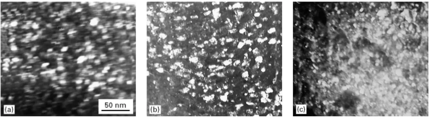
Figure 3 TEM dark-field images of A-films deposited at (a) 250 °C, (b) 400 °C and (c) 700 °C.
Figure 2 TEM electron diffraction patterns of A-films deposited at (a) 200 °C, (b) 250 °C and (c) 500 °C. Figure 1 XRD spectra of A-films grown at various deposition
temperatures.
Crystallinity of the grown films was examined by X-ray diffraction (XRD) and transmission electron microscopy (TEM). The film thickness was deter-mined from cross-sectional TEM images. The refrac-tive index of the film was measured by an ellipsometer using the 632.8 nm line of an He—Ne laser. The dielec-tric properties were studied by 1 MHz capacitance— voltage (C—») measurement using the Keithley model-82 CV measuring system, and the leakage current by HP4145B.
3. Results and discussion
3.1. Structural properties
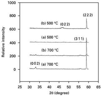
The structure of as-deposited films was examined as a function of deposition temperature. Fig. 1 shows XRD spectra of the A-films grown at various depo-sition temperatures. The A-films deposited at low tem-peratures ((300 °C) are mainly (2 2 2) oriented and those deposited above 500 °C appear to have extra (0 0 2) and (3 1 1) diffraction peaks in their spectra. Generally speaking, the intensity of the (2 2 2) peak does not tend to decrease as the temperature is in-creased. The appearance of extra diffraction peaks indicates that the films grown at higher temperatures exhibit more random orientation. Yoshimoto et al. have shown that CeO2 films grown on oxide-free (1 1 1) Si had (1 1 1) preferred orientation [16]. In this study the as-deposited films were polycrystalline and had (2 2 2) preferred orientation, like those reported previously. The minor grains with other orientations on the film are ascribed to grown SiO2. It is well known that a fresh Si surface would be easily covered by silicon oxide on exposure to the air. This as-grown amorphous SiO2 generally inhibits the epitaxial growth of any following layer.
Fig. 2 shows TEM electron diffraction patterns of the A-films grown at various deposition temperatures. The film deposited at 200 °C shows the coexistence of amorphous halo diffraction and obscure polycrystal-line rings. The film deposited at 250 °C is crystallized (Fig. 2b) and those grown at a temperature of 500 °C or higher are polycrystalline (Fig. 2c). Overlap of Si diffraction spots on the polycrystalline rings reveals that the films exhibit an exact fluorite structure be-cause CeO2 is lattice-matched with Si.
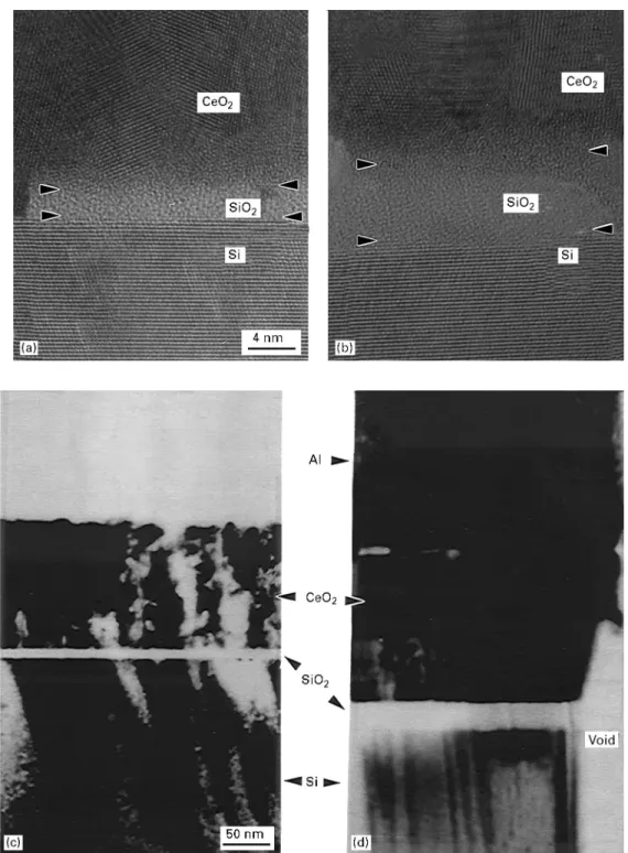
Figure 4 Cross-sectional TEM images for A-films deposited at (a) 300 °C (b) 700 °C and for B-films deposited at (c) 500 °C and (d) 700 °C. An
amorphous SiO2 layer is formed between the film and the Si substrate. Fig. 3 shows TEM dark-field images on (0 0 2) rings of the A-films grown at 250 °C, 400 °C and 700 °C, respectively. Although XRD spectra of the A-films grown at higher temperatures show stronger polycrys-tallinity, the sizes of (0 0 2) oriented grains on TEM images do not become larger as the deposition tem-perature increases. Calculations based on XRD peak broadening indicate the grain size in the film is about 26 nm, consistent with Fig. 3.
Fig. 4 shows the cross-sectional TEM images of the A-films deposited at 300 °C and 700 °C. Notice the amorphous SiO2 layer underneath the as-deposited film. This was generally observed during deposition or post-annealing of oxide film on Si [17, 18]. The vari-ation of SiO2 thickness with deposition temperature is illustrated in Fig. 5. The SiO2 thickness is around
2.6—3.6 nm up to a deposition temperature of 600 °C. Compared to the 100 nm thick CeO2 film, the SiO2 layer with thickness less than 4.0 nm is thin, which is not considered an effective insulator if an electric field is applied across the MIS capacitor. The fresh Si wafer is considered to grow SiO2 of no more than 1.0 nm in thickness before thin film growth based on the results of Fenner et al. [19]. All SiO2 layers in our study are thicker than 1.0 nm, so additional SiO2 grows during the deposition of CeO2 films. Fig. 4 indicates that the SiO2—Si interface is atomically sharp and clear but the CeO2—SiO2 interface is somehow not as clear. The CeO2—SiO2 interface is even more ambiguous; this is because the A-film grows at higher temperature (Fig. 4b). The ambiguous interface may be attributed to the increased interdiffusion between CeO2 and Si.
TA B LE I Dielectric constant (e3), flatband voltage (»FB), density of fixed oxide charge (N&), density of interface trapped charge (D*5), flatband voltage shift (*»FB) (evaluated from C—» curves) and leakage current density (at 0.4MVcm~1) for A-films and B-films prepared at various deposition temperatures
Growth condition e3 »FB (V) N& (cm~2) D*5 (eV~1cm~2) *»FB (V) J (A cm~2)
A, 700 °C 8.32 !3.25 1.15]1012 3.3 ]1012 0.12 1.3]10~8 A, 600 °C 7.2 !2.39 0.37]1012 0.72]1012 0.30 6.0]10~7 A, 500 °C 7.7 !1.55 0.22]1012 0.29]1012 1.18 1.1]10~6 A, 400 °C 6.9 !1.54 0.19]1012 0.27]1012 1.34 4.6]10~7 A, 300 °C 4.7 !1.43 0.17]1012 0.22]1012 1.92 1.1]10~7 A, 200 °C 5.9 !1.38 0.15]1012 1.22]1012 3.50 3.8]10~8 B, 500 °C, 30/1! 22.9 !7.5 3.72]1012 2.55]1012 0.28 2.0]10~7 B, 500 °C, 3/1! 22.8 !7.9 5.03]1012 8.98]1012 0.23 2.3]10~8 B, 700 °C, 30/1! 18.8 !2.98 1.29]1012 16.0 ]1012 0.37 2.5]10~8 B, 700 °C, 3/1! 24.6 !3.55 1.32]1012 7.99]1012 0.12 2.3]10~8
! Argon/oxygen flow rate ratio.
Figure 5 (d)Thickness of the SiO2 layer and (s) refractive index of
A-films as a function of deposition temperature.
Figure 6 XRD spectra of B-films deposited with argon/oxygen flow
rates in the ratios (a) 30/1 and (b) 3/1. Fig. 6 shows that the B-films grown at 500 °C and
700 °C also reveal (2 2 2) dominant diffraction in their XRD spectra and other diffraction peaks, e.g. (0 0 2), (3 1 1) and (0 2 2), are not greatly enhanced compared with Fig. 1. Therefore, the introduction of oxygen dur-ing deposition does not change the crystal orientation of as-grown B-films. One feature of the grown B-films is a drastic thickness increase of the SiO2 layers com-pared with the A-films (Fig. 4c and d). SiO2 layers with thicknesses of 11.0 nm and 32.0 nm are observed be-neath the B-films.
3.2. Refractive index
Variation of the refractive index with deposition tem-perature is shown in Fig. 5. The refractive index of CeO2 is not affected by the interfacial SiO2 layer, which is too thin compared with the thickness of CeO2 film deposited up to 600 °C. The refractive index approximately follows a monotone increase with de-position temperatures lower than 500 °C, remains at 2.46 in the range 500—650 °C and has fallen to below 2.38 at a deposition temperature of 700 °C. The refrac-tive index of the thin film depended significantly on the measuring wavelength [2, 3]. It might also have
been influenced by any change in the film crystallinity, the refractive index of the films presumably improved with a higher degree of structural ordering [20]. How-ever, only a small change in the refractive index was observed within the deposition temperature range, from 2.32 at 250 °C to 2.46 at 500 °C. XRD spectra reveal more diffraction peaks for films grown at higher deposition temperature (Fig. 1). Thus the small increase in the refractive index of A-films with increas-ing deposition temperature seems to be related to the polycrystallinity of the films. The slight decrease of the refractive index at 700 °C can be ascribed to the thickened SiO2 layer, as shown in Fig. 5.
3.3. Current—voltage characteristics
The leakage current was measured by the change of negative bias on the top Al electrode such that p-type Si substrate was in accumulation and there was elec-tron injection from the Al gate into the CeO2. The leakage current density in those as-deposited films is generally high and it tends to increase with increasing deposition temperature, as shown in Table I. The lower leakage current of the A films grown at above 600 °C can be ascribed to the thickened SiO2 layer, as
Figure 7 Leakage current as a function of inverse temperature and
bias voltage for A-films deposited at 500 °C: (s) bias voltage"2 V, (h) 4 V, (n) 6 V, (£) 8 V, (e) 10 V.
Figure 9 The I—» curves of Fig. 8 replotted using ln » as the
hori-zontal axis: (h) negative bias and (s) positive bias.
Figure 8 I—» curves with (h) negative and (s) positive bias
volt-ages for A-films deposited at 300 °C. shown in Fig. 5. A good insulator, the SiO2 layer
compensates for the relatively high leakage current of many high dielectric constant MIS gate oxides such as Ta2O5 and Y2O3 [21, 22]. Since the formation of SiO2 on silicon is generally observed in a conventional sputter system, thickness control of the SiO2 layer is important to maintain the overall dielectric constant above a suitable high value. Fig. 7 shows an Arrhenius plot of current through an MIS diode with CeO2 gate oxide (A-film) grown at 500 °C. The current density (JS) is independent of the measurement temperature below 200 K; this implies tunnelling or field emission conduction for current transport through the oxide. The current density follows an exponential relation-ship with measurement temperature above 200 K,
JSJexp(!E!/k¹) , where E!"0.32eV is the
activa-tion energy estimated from the data. This value agrees with those reported by others, confirming electrons as the charge carriers through CeO2 [4, 7].
Fig. 8 shows both the negative and positive biased
I—» characteristics for the A-films deposited at 500 °C.
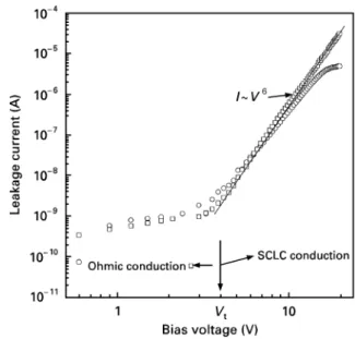
The I—» curves at low applied voltage show an ohmic-like characteristic. The positive bias current saturates above 16 V and the negative bias current does not saturate at the highest applied voltage of 20 V (corres-ponding to 2 MV cm~1). All the films show rapidly increasing leakage current at applied negative volt-ages of around 5—10 V followed by more slowly increasing leakage current at voltages above 10 V. Fig. 9 takes the I—» curves of Fig. 8 and replots them using lnV as the horizontal axis. The best fit to the curve is a power-law relation, IJ»`g whereg"6.
Among the commoner basic electrical conduction mechanisms, the only one that appears to match this empirical formula is space-charge-limited current (SCLC) conduction [23, 24]. The space charge is built up when the rate of carrier injection from the contact exceeds the rate at which the carriers can be trans-ported across the film. For SCLC conduction to oc-cur, at least one contact must be ohmic. Thus Ohm’s law is obeyed at very low densities of the injected
carrier, but the relationship between current and volt-age is non-linear at higher field and the SCLC conduc-tion follows a square law, IJ»2. The I—» curve transfers from ohmic conduction to SCLC conduction at a transfer voltage (»5) as shown in Fig. 9. However, if many sets of traps are distributed throughout the energy gap of the oxide, the injected carriers are re-moved by empty traps, so the SCLC is reduced.
Mark and Helfrich have shown that SCLC conduc-tion limited by exponentially distributed traps satisfies the I—» relation IJ»n`1 where n"¹#/¹ and ¹# is the characteristic temperature of the trap distribution [25]. The transfer voltage »5 is given by »5"
qk¹#N/d2/e, where d is the oxide thickness [26]. Thus
in a space charge region with an exponential distri-bution of traps, the transfer voltage should vary with the square of d. In this study a distribution of trap levels is expected because a large amount of structural disorders exists in the polycrystalline film, as shown in
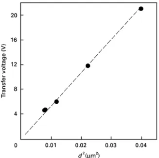
Figure 10 Transfer voltage as a function of the squared film
thick-ness.
Fig. 4, and it is reasonable to assume the I—» curve will not follow the simple square law. Fig. 10 shows that the transfer voltage varies linearly with the square of the A-film thickness up to 0.2lm. The results are consistent with SCLC conduction behaviour. Thus, it is concluded that I—» curves obey ohmic conduction at low voltages ((5 V) and exhibit SCLC conduction at high voltages ('5 V) as g"6. At even higher applied voltages ('16 V) , the current reaches satura-tion for a positive bias voltage. This saturasatura-tion arises from the limited number of electrons supplied by the p-Si to the insulator.
Current—voltage curves of B-films exhibit SCLC conduction similar to that for A-films (the curves are omitted for brevity). The leakage current for B-films is generally lower than for A-films, presumably due to the thicker SiO2 layers beneath the B-films. The only exception is the film deposited at 700 °C, which is yet to be explained.
3.4. Capacitance—voltage characteristics
The results of C—» measurements show that all the films exhibit typical MIS behaviour where regions of accumulation, depletion and inversion are present. Oxide capacitance of the films, i.e. MIS capacitance in accumulation, increases slightly with increasing de-position temperature. Table I lists related dielectric constants of the films calculated from the C—» measurements. The dielectric constants of CeO2 films given in Table I were obtained by deleting a serial SiO2 capacitor having a lower dielectric constant of 3.9. The variation of dielectric constant for A-films is similar to the change in refractive index (Fig. 5). The highest dielectric constant obtained for the A-films deposited at 500 °C is lower than the value for bulk CeO2. Introduction of oxygen during deposition dra-matically improves the dielectric constant of the grown films; the highest dielectric constant of B-films approaches the value of bulk CeO2.
The flatband voltage »FB corresponds to the flat-band capacitance (CFB) on the C—» curve; »FB exhibits a negative shift with increased deposition temperatures for A-films, as shown in Table I. This indicates that positive oxide charges in the A-films increase with increasing deposition temperature. The crystallinity of the A-film is improved by increasing the deposition temperature, so an increase of oxide charge in CeO2 films is not expected. Therefore, we relate the change of »FB to a thickness change of the interfacial amorphous SiO2 layer with increasing de-position temperature. It appears the oxide charges dominating »FB are mainly contributed by the amorphous SiO2 layer. »FB is readily related to the fixed oxide charge density (N&) by the relation »FB"/.4!qN&/C0, where /.4 is the work function difference between the Al gate and silicon and C0 is the oxide capacitance in accumulation [27]. As shown in Table I, N& increases with increasing deposition tem-peratures for the A-films. Thin film deposited at 200 °C with amorphous phase in the majority does not have higher N&.
It has been reported that SiO2 layers grown on Si at higher deposition temperatures exhibit lower N& [28]. Our B-films are consistent with this tendency, perhaps due to a thicker SiO2 layer, but our A-films appear to differ. Since N& is obtained from »FB, which relates to properties of the SiO2 layer, the different tendency in
N& varied with increasing deposition temperature and
may be attributed to the different properties of the SiO2 layer grown under the two different conditions, A and B. It is probable that N& in SiO2 is increased by the enhanced interdiffusion between CeO2 and SiO2 at high deposition temperatures. Note that N& for the B-films is apparently larger than for the A-films, as shown in Table I, due to the introduction of oxygen during sputtering. Similar results have been clearly observed for thermally grown SiO2 on Si [27, p. 245], thus it is reasonable to suggest that interfacial SiO2 dominates the variation of »FB and N& in our films.
At the flatband voltage, the interface-trapped charge density D*5 is given by
D*5"(C0!CFB) CFB[3qk¹A(dC/d»)]~1
!C20[Aq2(C0!CFB)]~1
where dC/d» is the slope at »FB, and A is the electrode area. D*5 at »FB is listed in Table I. It is found that for A-films an increase in deposition temperature leads to higher D*5, like N&. It has been observed in RF sput-tered strontium titanate thin films on Si that an in-creasing D*5 depends on the promoted formation of an interfacial SiO2 layer during the deposition [29]. The existence of an SiO2 layer would increase defect densi-ties along with trapping centres and surface states at the interface regions. The A-film deposited at 200 °C somehow shows a remarkably higher D*5 than the others deposited at the higher temperatures, except 700 °C. This high D*5 might be ascribed to the crystal-linity of the film because the film deposited at 200 °C is partly amorphous.
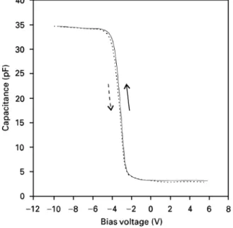
Fig. 11 shows 1 MHz C—» plots for MIS capacitors with gate oxides (A-film) deposited at 700 °C in which
Figure 11 Hysteresis in the 1 MHz C—» behaviour of the
Al—CeO2—p-Si MIS structure for A-films grown at 700 °C. the voltage is swept continuously as the arrows indi-cate. Films on p-type silicon show a carrier-injection-type hysteresis (counterclockwise rotation), where charges are injected from the silicon surface to trap-ping centres in the deposited film. A higher defect concentration in the film of lower crystallization is expected to create a large number of trapping centres, which may accommodate more electrons (trapped charge) injected from the electrode, causing a greater shift of the flatband voltage (*»FB) in hysteresis curves of C—» measurements. Table I shows that *»FB is more relevant for A-films deposited at lower temper-atures. A-films deposited at higher temperatures seem to exhibit lower amounts of trapped charge injected into the films during the bias cycle. This implies better crystallinity in the films grown at higher temperatures. B-films have lower*»FB than most A-films as illus-trated in Table I. This can be ascribed to their better crystallinity (higher dielectric constant) and their thick SiO2 layer [30].
Although the dielectric constant of CeO2 films can be increased to over 20 by introducing oxygen into the plasma, this does cause the formation of thick SiO2 layers, which lower the overall dielectric constant of CeO2—SiO2 composite layers. The dielectric constant for B-films including SiO2 layers is around 17. This lowering of the dielectric constant is unfavourable for DRAM capacitors. Methods to grow CeO2 films with high dielectric constant, while suppressing SiO2 growth are therefore expected. A high oxygen diffu-sion resistance bottom electrode on Si is more feasible for growing high dielectric constant CeO2 films with thin SiO2 layers. On the other hand, perhaps due to the polycrystallinity of the films, the leakage current of our CeO2 films is two orders of magnitude higher than for epitaxial CeO2 films grown by Tye et al. [31]. However, with respect to their application in gigabit DRAM dielectrics, a leakage current density of less than 1]10~7 A cm~2 at 1 V is required [32], thus our films are quite satisfactory.
4. Summary
CeO2 film deposited by RF magnetron sputtering above 250 °C is polycrystalline whereas film deposited below 200 °C is partly amorphous. An amorphous SiO2 layer is observed between CeO2 film and silicon. When the film is grown without oxygen flow and at higher temperatures, the dielectric constant increases up to 500 °C, but it remains as low as 6—8 in compari-son with 26 for bulk CeO2. When the film is grown under oxygen flow, its dielectric constant can be dras-tically improved to over 20. Results of C—» measure-ments show that the densities of interface-trapped charge and fixed oxide charge in the films increase with increasing deposition temperature. These two charge densities appear to be dominated by the as-grown SiO2 layer. I—» measurements indicate that the electrical conduction is well fitted by a power-law relation; this can be explained by SCLC conduction with distributed traps in the energy gap of the oxide.
Acknowledgement
The authors gratefully acknowledge financial support from the National Science Council of China under contract NSC 85-2112-M009-037.
References
1. W. J. C O LE MAN ,Appl. Opt. 13 (1974) 946.
2. R . P . N E T T E R F IE L D , W . G . S A I N T Y , P . J . M A R T I Nand S. H . SI E ,ibid. 24 (1985) 2267.
3. K. B . S U N DA R A M , P . F . W A H I DandP . J . S I S K ,¹hin Solid
Films 221 (1992) 13.
4. G. B O U R E A U , O . M A S MO U D IandR . T E T O T ,Solid State Commun. 79 (1991) 299.
5. H. L . T U L L E RandA . S . N O WI C K ,J. Electrochem. Soc. 126
(1979) 209.
6. A . M A R T I N E Z - A R I A S , J . S O R I A , J . C . C O N E S A , X . L . SE O A N E , A . A R C O Y AandR . C A T A L U N3 A,J. Chem. Soc. Faraday ¹rans. 91 (1995) 1679.
7. H. - J. B E I Eand A . G N O® R I C H ,Sensors and Actuators B4
(1991) 393.
8. M. W. D E N H O F FandJ . P . M c C A F F R E Y ,J. Appl. Phys. 70
(1991) 3986.
9. S. S . L E EandD . Y O UM ,Physica C 211 (1993) 205.
10. W . L . H O L S T E I N , L . A . P A R I SI , D . W. F A C E , X . D . WU , S. R . F O L T Y Nand R . E . M U E N C H A U S E N ,Appl. Phys.
¸ett. 61 (1992) 982. 11. T . N A K A Z A W A , T . I N OU E , M . S A T O Hand Y . Y A M A -MO T O ,Jpn. J. Appl. Phys. 34 (1995) 548. 12. T . H I R A I , K . T E R A M O T O , K . N A G A S H IM A , H. K O I K E andY . T A R U I,ibid. 34 (1995) 4163. 13. A . G . F R A N GO U L , K . B . SU N D A R A MandP . F . W A H I D ,
J. »ac. Sci. ¹echnol. B 9 (1991) 181.
14. W. C . T S A I H , C . K . H U A N GandT . Y . T SE N G ,J. Amer. Ceram. Soc. 78 (1995) 1969.
15. B . W I N D O W and N . SA V V I D E S , J. »ac. Sci. ¹echnol. A 4 (1986) 196.
16. M. Y O SH I M OT O , H . N A G A T A , T . T S U K A H A R Aand H. K O IN U M A ,Jpn. J. Appl. Phys. 29 (1990) L1199.
17. T . C H I K Y O W , S . M . B E D A I R , L . T Y Eand N . A . E L -MA S R Y ,Appl. Phys. ¸ett. 65 (1994) 1030.
18. T . I NO U E , T . OH S U N A , Y . O B A R A , Y . Y A MA MO T O , M. S A T O HandY . S A K U R A I ,Jpn. J. Appl. Phys. 32 (1993)
1765.
19. D. B . F E N N E R , D . K . B I E G E L S E NandR . D . B R I N G A N S,
J. Appl. Phys. 66 (1989) 419.
20. D. A . C H A N G , P . L I NandT . Y . T S E N G ,J. Appl. Phys. 78
21. S. B A N E R J E E , B . S H E N , I . C H E N , J . B O H L M A N , G. B R O W NandR . D O E R I N G ,J. Appl. Phys. 65 (1989) 1140.
22. A . C . R A ST O G IandR . N. S H A R M A ,J. Appl. Phys. 71 (1992)
5041.
23. S. M . S Z E ,‘‘Physics of Semiconductor Devices’’ (Wiley, New York, 1981) p. 403.
24. A . R O S E ,Phys. Rev. 97 (1955) 1538.
25. P . M A R KandW . H E L F R I C H ,J. Appl. Phys. 33 (1962) 205.
26. J . G . SI M M ON S ,in ‘‘Handbook of Thin Film Technology’’, edited by L. I. Maissel and R. Glang (McGraw-Hill, New York, 1970), p. 14.
27. D. K . S C H R O DE R , ‘‘Semiconductor Material and Device Characterization’’ (Wiley, New York, 1990) p. 225.
28. E . H . S N O W ,J. Electrochem. Soc. 114 (1967) 266.
29. J . R . B E L S I C KandS . B . KR U P A N I D H I,J. Appl. Phys. 74
(1993) 6851.
30. K. L E HO V E C ,Solid-state Elec. 11 (1968) 135.
31. L . T Y E , N . A . E L - M A S R Y , T . C H IK Y O W , P . M C L A R T Y andS. M . B E D A IR ,Appl. Phys. ¸ett. 65 (1994) 3081.
32. T . Y . T S E N G ,IEDMS, C2-5 (1996) 89.
Received 11 October 1996 and accepted 10 January 1997