國 立 交 通 大 學
應 用 化 學 研 究 所
博 士 論 文
以蒽為主體之非晶態材料雙極性載子傳輸特性與摻雜電性
研究及其在有機電激發光元件之應用
Study of Bipolar Charge Transport and Electrical Doping
Characteristics of Amorphous Anthracene-based Materials and Their
Applications in Organic Electroluminescence Devices
研 究 生:何孟寰
指導教授:陳金鑫 博士
陳登銘 博士
以蒽為主體之非晶態材料雙極性載子傳輸特性與摻雜電性研究及
其在有機電激發光元件之應用
Study of Bipolar Charge Transport and Electrical Doping
Characteristics of Amorphous Anthracene-based Materials and Their
Applications in Organic Electroluminescence Devices
研 究 生:何孟寰 Student:Meng-Huan Ho 指導教授:陳金鑫 博士 Advisor:Dr. Chin H. Chen 陳登銘 博士 Dr. Teng-Ming Chen
國 立 交 通 大 學 應 用 化 學 研 究 所
博 士 論 文
A Thesis
Submitted to Institute of Applied Chemistry College of Science
National Chiao Tung University in Partial Fulfillment of the Requirements
for the Degree of Doctor of Philosophy
in
Applied Chemistry August 2010
Hsinchu, Taiwan, Republic of China
I
以蒽為主體之非晶態材料雙極性載子傳輸特性與摻雜電性
研究及其在有機電激發光元件之應用
研究生:何孟寰 指導教授:陳金鑫 博士 陳登銘 博士 國立交通大學應用化學研究所 摘 要 將 p 型與 n 型有機摻雜層引入由 2-methyl-9,10-di(2-naphthyl)anthracene (MADN) 天藍光系統與黃光材料 rubrene 所組成的雙波段白光有機電激發 光元件結構中,並有效控制載子再結合區域於薄層發光層中,在亮度 1000 cd/m2下可得到高發光效率 10 cd/A 和 9.3 lm/W。利用有機摻雜層的 p-n 接 面作為連接層,也可以製作出高亮度的串聯式雙波段白光有機電激發光元 件。 但雙波段白光元件的色域與演色性無法達到全彩顯示器與固態照明應 用 的 需 求 。 於 是 我 們 開 發 出 以 2-methyl-9,10-di(1-naphthyl)anthracene (,-MADN) 為主發光體材料的高效率且穩定的深藍色發光系統並應用於II 三波段白光有機電激發光元件中,可得到高發光效率 8 cd/A 和寬廣的發光 頻譜,CIE 色度座標為(0.34, 0.35),色域及演色性也提升到 73.2 %和 87。 我們也利用飛行時間量測法來量測一系列以蒽(anthracene)為主體的材 料的載子傳輸特性,量測結果顯示這些材料具有極快的電洞載子遷移率, 其數值介於 2 × 10⁻³ to 9 × 10⁻³ cm2/Vs 之間。同時也發現能將 C60 應用於飛 行時間技術中作為電荷生成層,可大幅減少樣品中待測材料的厚度。 另一方面, 根據導納量測理論與有機材料高阻抗的特性,我們提出了 雙異質介面有機元件的導納等效電路模型,並用以研究 MADN 的 p 型與 n 型薄膜摻雜層電性。其結果顯示將氧化鎢(WO3) 與 氟 化銫 (CsF)摻雜於 MADN 中,可降低載子的注入能障以及元件的操作電壓。 最後,根據飛行時間量測法與導納分析的結果,我們設計出第一個以 MADN 為單一主體材料的高效率且穩定的有機電激發光元件。
III
Study of Bipolar Charge Transport and Electrical Doping
Characteristics of Amorphous Anthracene-based Materials and Their
Applications in Organic Electroluminescence Devices
Student:Meng Huan Ho Advisor:Dr. Chin H. Chen Dr. Teng-Ming Chen
Department of Applied Chemistry National Chiao Tung University
ABSTRACT
We demonstrated highly power-efficient di-chromatic white organic light-emitting diode (WOLED) devices composed of a sky blue doped emitter of 2-methyl-9,10-di(2-naphthyl) anthracene (MADN) and a yellow emitter of rubrene. By introducing p-doped and n-doped organic layers into the device architecture along with carefully controlling the carrier recombination zone in a thin layer thickness, the high efficiency of 10 cd/A and 9.3 lm/W at 1000 cd/m2 can be achieved. A high-brightness tandem di-chromatic WOLED device with a connecting layer of organic p-n junction was also fabricated.
But the color gamut and color rendering index (CRI) of di-chromatic WOLEDs are not adequate for full-color display and solid state lighting
IV
applications. Hence we developed an efficient and stable deep blue fluorescent system based on a host material of 2-methyl-9,10-di(1-naphthyl) anthracene (,-MADN) and adopted it to tri-chromatic WOLED devices. The color gamut and CRI of tri-chromatic WOLED device can be improved to 73.2% and 87, respectively, with high efficiency of 8.0 cd/A and a white CIEx,y coordinates of
(0.34, 0.35).
The hole mobilities of ADN-type material were also measured by time-of-flight technique, and it is found that ADN-type materials have high hole mobilities in the ranges of 2 × 10⁻³ to 9 × 10⁻³ cm2/Vs. C60 was also shown to be a useful charge generation layer and effectively reduces the layer thickness of test material for TOF measurements of hole mobilities of ADN-type materials.
We further investigated the electrical characteristics of MADN-based p-doped and n-doped organic layers by measuring current-voltage curves and temperature-dependent admittance spectroscopy. It was found that the conductive-doping can reduce the injection barrier and drive voltage when they are adopted in OLED devices.
Finally, according to all results disclosed in this thesis, an efficient and stable OLED device with simplified architecture based on a single common host of MADN was demonstrated for the first time with excellent performance.
V
Acknowledgements
自從 2001 年升大三的暑假專題研究接觸到 OLED 後,變和這個迷人 的技術結下了不解之緣。在研讀碩士與博士的這七年,最要感謝的是指導 教授陳金鑫博士的耐心指導,無論是實驗上或是生活上的啟發,都讓我獲 益良多,也感謝老師提供我多次參加國際會議的機會,尤其是在 SID 會議 上 oral 的經驗,更是大大拓展了我的視野及信心來迎接國際化的挑戰,謹 此致以最衷心之敬意與感激。也很感謝共同指導教授陳登銘博士在我博士 班期間的指導與鼓勵。此外,感謝口試委員謝宗雍教授、陳方中教授、吳 忠幟教授、李重君博士以及湯舜鈞博士對本論文所提出的建議以及指導, 使學生在研究的方向及態度上更臻成熟。 加入OLED實驗室已九年,期間認識了許多同甘共苦的好夥伴,無論在 學術上或生活上都有豐碩的收穫。首先要特別好夥伴士峯學長、曜杉學長、 班如曼(Dr. B. Banumathy),你們的支持是我面對挑戰的勇氣來源。感謝電 子物理所的謝明達博士對本論文中導納圖譜的量測、等效電路模型的建立 和實驗結果的討論。另外感謝學長孝文、榮安、世文、世男、孟庭、在我 遇到困難時給我的建議和鼓勵。也感謝實驗室的其他伙伴們的互相扶持, 沒有大家實驗成果的分享以及討論,也不會有後續的進步。另外,還要感 謝實驗室助理美貞、克瑜在行政事務方面的熱心幫忙。VI
最後最感謝我的家人讓我無後顧之憂,可以專心地學習,也謝謝你們的 陪伴,有你們在背後支持,是激勵我前進的原動力,我會更加的努力,謹 以此論文獻給我最愛的你們。
In addition, I was really lucky to be a visiting student in University of Rochester, NY, USA, under the supervision of Prof. Ching W. Tang for one year, who is the inventor of OLED technology. I appreciate Prof. Ching W. Tang for his insightful advice on both an academic and personal level. Prof. Tang’s example of diligence, persistence, and insight has inspired me, and his guidance has also enabled me to understand the attitude for pursuing the truth. I would also like to thank Dr. David Weiss, Dr. Jason U. Wallace, Matthew J. Smith, Thomas Yung-Hsin Lee for their help of TOF experiments and discussions. I also would like to extend my thanks to my fellow graduate students who were always helpful in life and experiments. This includes Wei Xia, Sunny Hsiang-Ning Wu, Hao Lin, Hui Wang, Min-Lu Zhang, Sang-Min Lee, Lichang Zhen, Jonathan Welt, Eric Glowacki, and Mark Hsu.
VII
Table of Contents
Chinese Abstract……….…I English Abstract………...III Acknowledgements………..………V Table of Contents……..……….……VII List of Figures...XIII List of Table...………..XXIIChapter 1 Introduction of Organic Light-Emitting Diodes……….1
1.1 General overview of Organic Light-Emitting Diodes...1
1.2 Full-color techniques for OLED display………..3
1.2.1 RGB side-by-side pixilation………...3
1.2.2 WOLED backlight with color filter…………...……….4
1.2.3 Blue OLED backlight with color-changing medium………..5
1.3 WOLEDs for lighting applications………...………6
1.4 p-i-n OLEDs………...8
1.5 Tandem OLEDs………..11
1.6 Thesis organization……….13
References………..………..14
Chapter 2 Experimental Details and Analytical Methods……….18
2.1 Overview………18
2.2 Materials used in this thesis………18
VIII
2.3.1 UV absorption and photoluminescence spectra………21
2.3.2 Thermal properties………21
2.3.3 Electrochemical properties and HOMO/LUMO energy levels…21 2.3.4 Fluorescence quantum yield……….22
2.4 Fabrication process of OLED devices………22
2.4.1 Cleaning procedure of ITO-glass substrate………..22
2.4.2 Vacuum thermal evaporation of patterned films………...23
2.4.3 Characterization of device performance………...24
2.4.4 Encapsulation and stability measurement……….24
2.5 Charge transport mechanism in disordered organic materials…………25
2.6 TOF measurement...28
2.7 Non-dispersive and dispersive transit signals……….31
2.8 Experiments of TOF measurement……….…32
2.9 Introduction of impedance spectroscopy and admittance spectroscopy.33 2.10 Model for thermal admittance spectroscopy study………...36
2.11 Experiments of temperature-dependent AS measurement………..…..38
References…………..………..39
Chapter 3 Development of Di-Chromatic White Organic Light-Emitting Diodes………..…..…42
3.1 Introduction………42
3.2 Characteristics of white light………..43
3.2.1 CIE 1931 chromaticity diagram………43
3.2.2 Color Temperature………44
IX
3.3 Performances of state-of-the-art WOLEDs………45
3.4 Conventional di-chromatic WOLED device………...……...47
3.5 Development of p-i-n di-chromatic WOLED device………....….50
3.6 Development of tandem p-i-n di-chromatic WOLED device………….57
3.7 Summary……….62
References………..………..64
Chapter 4 Development of Fluorescence Deep Blue System and Tri- Chromatic White Organic Light-Emitting Diodes………...67
4.1 Introduction………67
4.2 Prominent blue fluorescence OLED materials based on anthracene core structure………...69
4.3 Development of host material for deep blue emitter………..76
4.4 Energy transfer between blue host-guest materials………80
4.5 Device performances of deep blue OLED devices……….83
4.6 Development of tri-chromatic WOLED device……….87
4.7 Summary………...93
References………..………..………96
Chapter 5 Carrier Transport Properties of Anthracne-Based Materials...100
5.1 Bipolar nature of anthracene-based materials………..100
5.2 Mobility measurements of anthracene-based materials in literatures..106
5.3 Mobility measurements of anthracene-based materials by TOF technique………..………..111
X
5.3.2 TOF results of MADN………113
5.3.3 TOF results of TBADN………..116
5.3.4 TOF results of ADN………117
5.3.5 Discussions……….118
5.4 Using buckminsterfullerene (C60) as charge generation layer……….121
5.4.1 TOF results of MADN with C60 as CGL………...123
5.4.1 TOF results of TBADN with C60 as CGL……….124
5.4.3 Discussions……….124
5.5 Summary………...126
References………..………126
Chapter 6 Admittance Spectroscopy Measurements for Conductive-Doped Organic layers………130
6.1 Introduction………..130
6.2 n-type doped system composed of PAK2-doped BPhen………..131
6.2.1 Admittance measurements of PAK2-doped BPhen layer…..….143
6.2.2 Elucidation of the mechanism of thermal-evaporated PAK2 layer….………..141
6.2.3 Device performances of using n-doped layer composed of PAK2-doped BPhen..……….148
6.3 p-type doped system composed of WO3-doped MADN……...151
6.3.1 Admittance measurements of WO3-doped MADN layer………152
6.3.2 Device performances of using p-doped layer composed of WO3-doped MADN………...………...157
XI
6.4.1 Admittance measurements of CsF-doped MADN layer…...159
6.4.2 Device performances of using n-doped layer composed of CsF-doped MADN………162
6.5 Summary………...163
References..………164
Chapter 7 Organic Light-Emitting Diodes based on one Multifunctional Bipolar Material………167
7.1 Introduction………..167
7.2 Review of anthracene-based materials used in HTL of OLED devices………...……….169
7.3 Using MADN as HTL...171
7.3.1 Admittance measurements of MADN/Alq3 bilayer structure….171 7.3.2 Device performances of using MADN as HTL...174
7.4 Review of anthracene-based materials used in ETL of OLED devices………...……….178
7.5 Using MADN as ETL…………...……….181
7.5.1 Electrical characteristics of electron-only devices………..181
7.5.2 Device performances of using MADN as ETL...…………...183
7.6 Single-layer OLED devices based on multifunctional bipolar MADN……….183
7.7 Stable and efficient p-i-n OLED devices with a single common host of MADN……….186
7.7.1 p-i-n blue OLED device based on MADN……….186
XII
7.8 Summary………...189
References...………190
Chapter 8 Conclusions and Future Works…...194
8.1 Conclusions………..194
8.2 Future works………...……….195
References...………196
Curriculum Vitae………...198
XIII
List of Figures
Figure 1-1 Schematic representation of RGB side by side pixilation…...………4
Figure 1-2 Full-color OLED techiniques………...………...5
Figure 1-3 Lighting Co’s announced WOLED mass production…………...…...6
Figure 1-4 UV-VIS-NIR absorption spectra of pure and WO3 doped 2-TNATA thin films……….………...9
Figure 1-5 (a) Configuration of OLED with Cs2CO3 as electron injection layer and J-V characteristics. (b) Configuration of OLED with co- evaporated EIL and J-V characteristics……….10
Figure 1-6 Common p-i-n OLED device structure and energy diagram……...11
Figure 1-7 Comparison of single-unit device and tandem device…………...…11
Figure 1-8 (a) Calculated luminance enhancement vs the number of emitting units. (b) Calculated power efficiency (lm/W, normalized to that of the reference device) for both noncavity and cavity tandem device.13 Figure 2-1 Schematic representation of device pattern……...………23
Figure 2-2 Schematic diagram of vacuum thermal coater……….………..24
Figure 2-3 Schematic diagram of an encapsulated OLED device………...25
Figure 2-4 Schematic diagram of device lifetime measurement……….25
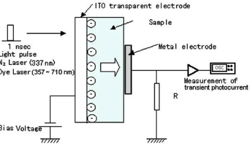
Figure 2-5 Typical TOF configuration………29
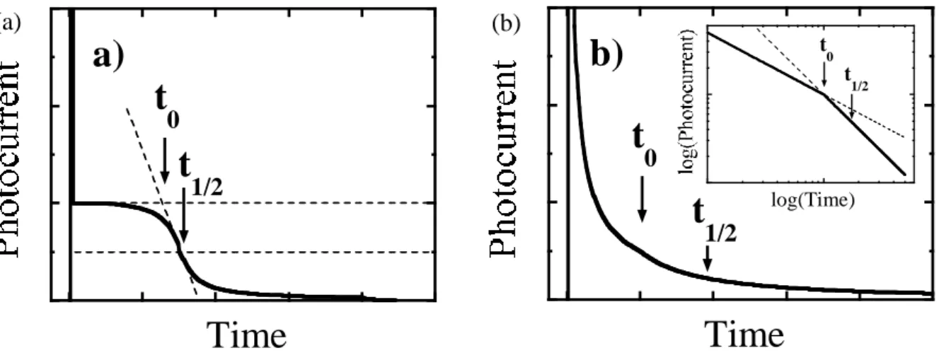
Figure 2-6 Example TOF transit signals for (a) non-dispersive curve, and (b) dispersive curve with an inset of a log-log scale………..……...….32
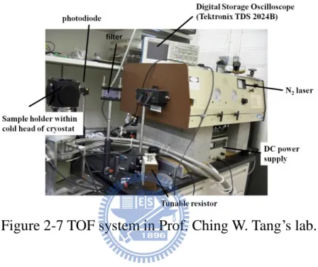
Figure 2-7 TOF system in Prof. Ching W. Tang’s lab………...33
Figure 2-8 Graphical representation of the complex impedance plane………...34 Figure 3-1 CIEx,y chromaticity diagram. All the colors in the visible spectrum lie
XIV
within or on the boundary of this diagram. The internal arc is the Planckian locus, which is the plot of the coordinates of black body radiation at the temperatures shown, described as color-correlated temperatures………..………44 Figure 3-2 Conventional WOLED device architecture and molecular structures
of key materials………...………47 Figure 3-3 (a) EL spectrum at 20 mA/cm2 and (b) CIEx,y coordinates vs current
density characteristics of conventional WOLED device.……...48 Figure 3-4 (a) The transmittance of RGB color filters and EL spectrum of
conventional WOLED device. (b) Spectra of RGB colors after attaching color filters. (c) The color gamut of NTSC standard and
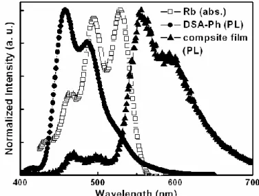
conventional WOLED device………49 Figure 3-5 Schematic device architecture of p-i-n WOLEDs……….51 Figure 3-6 Absorption spectrum of Rb and solid PL spectra of DSA-Ph and composite thin film………52 Figure 3-7 (a) Solid PL spectrum of composite film and EL spectra of device I at 20 mA/cm2. (b) CIEx,y coordinates vs current density characteristics
of device I………..53 Figure 3-8 (a) J-V characteristics of devices I and II. (b) Solid PL spectrum of composite thin film and EL spectra of device I and II at 20 mA/cm2. (c) CIEx,y coordinates vs current density characteristics of device I
and II………..55 Figure 3-9 (a) EL spectra at 20 mA/cm2. (b) CIEx,y coordinates vs current
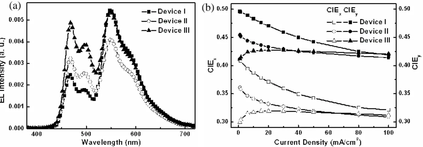
density characteristics of devices I, II, and III………...56 Figure 3-10 L-J-V characteristics of conventional white device and device III..59
XV
Figure 3-11 Device architecture of devices III and IV………59 Figure 3-12 Transmittance spectrum of BPhen: Cs2CO3 (20 nm) /NPB: WO3 (70
nm) thin film………60 Figure 3-13 (a) L-J-V and (b) current efficiency and external quantum efficiency vs current density characteristics of devices III and IV…………...60 Figure 3-14 (a) EL spectra at 20 mA/cm2 and (b) CIEx,y coordinates vs
luminance characteristics of devices III and IV………..61 Figure 3-15 (a) Normalized EL intensity vs viewing angle characteristics of devices III and IV. (b) EL spectra of device IV under viewing angles
of 0°, 30°, and 60° off the surface normal………...62 Figure 4-1 Structures of anthrecene-based blue host materials………...71 Figure 4-2 AFM imagines of (a) ADN and (b) MADN after annealing at 95 0C for 1 hr...74 Figure 4-3 (a) EL efficiency and (b) device stability comparisons of ADN,
TBADN, and MADN...75 Figure 4-4 AFM topographic images of -MADN thin film deposited on
silicon wafers (50 nm) after heating at 95 °C for 1 hr………...78 Figure 4-5 Normalized absorption and fluorescence spectra of MADN and
-MADN in toluene………...79 Figure 4-6 Cyclic voltammograms of MADN and -MADN……….80 Figure 4-7 Absorption spectrum of SA-BiPh and emission spectra of MADN
and ,-MADN in toluene………82 Figure 4-8 Thin-film solid PL spectra of SA-BiPh doped MADN and ,-
MADN in PMMA………..82 Figure 4-9 Energy diagrams of (a) electron-only and (b) hole-only devices…..85
XVI
Figure 4-10 J-V characteristics of (a) electron-only devices and (b) hole-only devices……….85 Figure 4-11 Device operational stability of the blue devices………..86 Figure 4-12 EL spectrum of 2BpSA-BiPh doped deep blue device at 20
mA/cm2………88 Figure 4-13 (a) EL spectrum of B/G/R device at different current density. (b) CIEx,y coordinates vs current density characteristics of B/G/R
device………..………...89 Figure 4-14 Energy diagram of B/G/R device………...90 Figure 4-15 (a) EL spectrum of R/B/G device at different current densities. (b) CIEx,y coordinates vs current density characteristics of R/B/G
device………...91 Figure 4-16 EL spectra of tri-chromatic white devices at 20 mA/cm2………....92 Figure 4-17 Device operational lifetime of B/G/R and p-i-n R/G/B devices…..93 Figure 4-18 (a) The transmittance of RGB color filters and EL spectra of
di-chromatic and tri-chromatic WOLEDs. (b) Spectra of RGB colors after attaching color filters. (c) The color gamut of
di-chromatic and tri-chromatic WOLEDs……….…..95 Figure 5-1 Calculation model of the reorganization energy………..102 Figure 5-2 Evolution of the internal reorganization energy in oligoacenes as a
function of the inverse number of rings, as calculated at the density functional theory level for holes (●) and electrons (■), and estimated as twice the relaxation energy extracted from gas-phase UV
photoelectron spectroscopy measurements (○) for holes...103 Figure 5-3 Chemical structures of aryl-substituted anthracene derivatives and
XVII
triphenylamine-substituted anthracene derivatives……….106 Figure 5-4 (a) TOF transient signals of ADN, TBADN and TTBADN at 290K
under applied field strengths of 0.56, 0.58, and 1.45 MV/cm, respectively. (b) field dependent electron and hole mobilities of ADN, TBADN, DTBADN and TTBADN at 290 K………...107 Figure 5-5 The frontier orbitals of (a) ADN and (b) TTBADN………108 Figure 5-6 (a) Chemical Structure of terfluorene. (b) Representative TOF
transients for holes of ADN at E = 3.3 × 10⁵ V/cm. (c) Hole
mobilities vs E1/2 of ADN………109 Figure 5-7 (a) Chemical Structure of ANF and ADF. (b) Steady-state EL
spectrum of a typical transient OLED. Inset: transient OLED device structure. (c) Frequency-dependent EL quenching upon application of 8 V square-wave DC voltage pulses of increasing frequency, 50% duty cycle; solid curves represent the best fits to polynomials…...110 Figure 5-8 Absorption spectra of MADN film………..112 Figure 5-9 The relationship of transmitted light intensity at 337 nm and
absorption depth of MADN film……….113 Figure 5-10 Representative TOF transient for holes of MADN at (a) E = 3.7 ×
105 V/cm (8.1 m). (b) E = 3.69 × 10⁵ V/cm (14.9 m). (c) Hole mobilities vs E1/2 of MADN………..114 Figure 5-11 Representative TOF transient for electrons of MADN (14.9 m) at
E = 2.01 × 10⁵ V/cm………..116 Figure 5-12 (a) Representative TOF transient for holes of ADN at E = 4.15 × 10⁵ V/cm. (b) Hole mobilities vs E1/2 of TBADN………..117
XVIII
Figure 5-13 (a) Picture of crystallized ADN sample. (b) Representative TOF transient for holes of ADN at E = 2.14 × 10⁵ V/cm……….118 Figure 5-14 Hole mobilities vs E1/2 of ,-MADN, MADN, and TBADN…..119 Figure 5-15 Absorption spectra of C60 film………..122 Figure 5-16 (a) Representative TOF transient for holes of MADN at E = 2.12 ×
105 V/cm. (b) Hole mobilities vs E1/2 of MADN………...123 Figure 5-17 (a) Representative TOF transient for holes of TBADN at E = 2.12 × 10⁵ V/cm. (b) Hole mobilities vs E1/2 of TBADN………...124 Figure 5-18 Hole mobilities vs E1/2 of MADN and TBADN………125 Figure 6-1 I-V characteristics of PAK2-doped electron-only devices………...134 Figure 6-2 (a) G/F-F spectrum and capacitance-frequency C-F spectrum of 5%
PAK2-doped device measured at 2 V and room temperature. (b) Schematic representation of equivalent circuit model……….135 Figure 6-3 G/F-F spectra of PAK2-doped electron-only devices at various
biases…………...………138 Figure 6-4 Temperature-dependent G/F-F spectra of 5% PAK2-doped devices
measured at various biases………..139 Figure 6-5 (a) Characteristics of ln(F) vs 1000/T of 5% PAK2-doped device at
various biases derived from the low-frequency peaks in Figure 6-4. (b) Relationship between Ea and applied bias of PAK2-doped
devices……….140 Figure 6-6 ∆f vs I characteristics of (a) NPB, (b) MADN, and (c) PAK2…….144 Figure 6-7 ∆f vs ∆M characteristics of NPB, MADN, and PAK2……….144
XIX
Figure 6-9 Relationship of mass change (∆m) vs time………..147 Figure 6-10 AFM topographic images of BPhen and 5% PAK2-doped BPhen
thin films deposited on silicon wafers (50 nm). (a) BPhen before heating; (b) BPhen after heating; (c) 5% PAK2-doped BPhen before heating; (d) 5% PAK2-doped BPhen after heating (scanned area: 5
m × 5 m).………...147 Figure 6-11 Power efficiency vs luminance characteristics of OLED devices.150 Figure 6-12 Device operational stability of devices C and D...150 Figure 6-13 Cyclic voltammogram of MADN by using 0.1M
tetrabutylammonium hexafluorophosphate as the supporting
electrolyte in dichloromethane………..151 Figure 6-14 I-V characteristics of WO3-doped hole-only devices……….153
Figure 6-15 G/F-F spectra at zero bias and room temperature of hole-only
Devices with various WO3 doping concentration………..154
Figure 6-16 Temperature-dependent G/F-F spectra at zero bias of hole-only devices with various doping concentration………...155 Figure 6-17 (a) Characteristic of ln(F) vs 1000/T of WO3-doped devices derived
from the low-frequency peaks in Figure 6-16. (b) Schematic energy diagram of ITO/p-doped MADN interface………155 Figure 6-18 L-J-V characteristics of the WO3-doped devices………...158
Figure 6-19 I-V characteristics of CsF-doped electron-only devices…………159 Figure 6-20 Temperature-dependent G/F-F spectra at zero bias of electron-only
devices with various doping concentration………...161 Figure 6-21 (a) Characteristic of ln(F) vs 1000/T of CsF-doped devices derived
XX
diagram of Al/n-doped MADN interface………..161 Figure 6-22 Device architecture of standard device and i-i-n devices………..162 Figure 6-23 Current efficiency vs current density characteristics of OLED
devices………...163 Figure 7-1 Chemical structures of anthracene-based HTLs...170 Figure 7-2 I-V characteristics of hole-only devices………...172 Figure 7-3 Temperature-dependent G/F-F spectra at zero bias of hole-only
devices (a) MADN and (b)NPB………..173 Figure 7-4 (a) Characteristic of ln(F) vs 1000/T of hole-only devices derived
from the low-frequency peaks in Figure 7-3. (b) Schematic energy diagram of ITO/MADN interface………174 Figure 7-5 Current efficiency vs current density characteristics of devices A, B,
F, and G………176 Figure 7-6 Absorption spectra of MADN and MADN radical cation in MeCN
solution………177 Figure 7-7 (a) Device operational stability of device G measured at different
current densities. (b) Extrapolated half life of device G………….178 Figure 7-8 Chemical structures of anthracene-based ETLs...180 Figure 7-9 I-V characteristics of electron-only devices……….182 Figure 7-10 L-J-V characteristics of green C545T-doped device utilizing MADN
as ETL………..……….183 Figure 7-11 Device architecture of green and blue OLED devices with MADN
as HTL and ETL………..………..185 Figure 7-12 (a) Device architecture and (b) energy diagram of p-i-n OLEDs with a single common host………..187
XXI
Figure 7-13 Device operational stability of standard p-i-n devices and common host p-i-n device………..188 Figure 7-14 (a) EL spectra at different current densities and (b) operational
XXII
List of Tables
Table 1-1 Comparisons of WOLED and other lighting sources…...….…………7 Table 2-1 Abbreviation, chemical structure and nomenclature of materials used in this thesis……….…18 Table 3-1 Performances of start-of-the-art WOLEDs……….46 Table 3-2 EL performances of p-i-n white OLED devices at 20 mA/cm2……...57 Table 3-3 EL performances of WOLED devices at 20 mA/cm2………..63 Table 4-1 PL and thermal properties of ADN derivatives………...75 Table 4-2 Thermal, optical, and electrochemical Properties of MADN and
-MADN……….78
Table 4-3 EL performances of blue devices at 20 mA/cm2……….83 Table 4-4 EL performances of tri-chromatic WOLED devices at 20 mA/cm2...92 Table 4-5 EL performances of WOLED devices at 20 mA/cm2………..94 Table 5-1 Theoretical evaluation of the reorganization energies (, eV) for hole
and electron transport for anthracene-based materials………..104 Table 5-2 The reported mobility data of ADN-type derivatives………111 Table 5-3 The fitted values of zero-field hole mobility, Poole-Frenkel factor, and relative film density of MADN and TBADN………119 Table 5-4 The fitted values of zero-field hole mobility and Poole-Frenkel factor
of MADN and TBADN…………..……….………..125 Table 6-1 Parameters of the linear fitting(∆f = K∆M +B) from Figure 6-7 (r is
the linear correlation coefficient)………..145 Table 6-2 EL performances of OLED devices at 20 mA/cm2………..….149 Table 6-3 EL performances of OLED devices at 20 mA/cm2………..….158
XXIII
Table 6-4 EL performances of OLED devices at 20 mA/cm2………..….163 Table 7-1 EL performances of OLED devices at 20 mA/cm2………..….175 Table 7-2 EL performances of OLED devices at 20 mA/cm2………..….186 Table 7-3 EL performances of OLED devices at 20 mA/cm2………..….188
1
Chapter 1
Introduction of Organic Light-Emitting Diodes
1.1 General overview of organic light-emitting diodes
The electroluminescence (EL) phenomenon was first discovered in a piece of carborundum (SiC) crystal by H. J. Round in 1907 [1]. Commercial research into light-emitting diodes (LEDs) technology started in early 1962, when Nick Holonyak Jr. created the first inorganic LED [2,3]. In 1950s, Bernanose first observed EL in organic materials by applying a high-voltage alternating current (AC) field to crystalline thin films of arcidine orange and quinacrine [4,5].
The direct current (DC) driven EL cell using single crystals of anthracene was first demonstrated by Pope and his co-workers following the discovery of LEDs made with III-V compound semiconductors [6]. Although the quantum efficiency of this device could reach 8%, the high drive voltage limited its practical application. In 1975, the first organic EL devices made with a polymer poly(N-vinyl carbazole) (PVK) were demonstrated [7]. In 1982, Vincett et al. [8] demonstrated the light-emitting devices fabricated by thermal evaporation of polycrystalline anthracene. The required voltage to generate light was significantly reduced due to the much thinner organic layer. However, in this device, carrier recombination zone was too close to one of the electrodes which limited its quantum efficiency to less than 0.1%.
In 1987, Tang and Van Slyke at Kodak introduced a double layered organic light-emitting device (OLED), which combined modern thin film deposition techniques with suitable materials and device structure to produce EL with moderately low bias voltages and significantly better luminance efficiency
2
[9,10]. Their research eventually led to the discovery of the first efficient multi-layered organic EL device based on the concept of the heterojunction architecture [10,11] which was followed by the discovery of the doped emitter using the highly fluorescent organic dyes for color tuning, efficiency and stability enhancement [12,13]. Shortly afterwards, in 1990 the Cambridge group led by Friend announced a conducting polymer-based PLED [14,15]. The polymeric thin films are fabricated by convenient wet-coating technology and permit deposition on various substrates [16,17,18,19,20].
Although the flat panel display (FPD) industry is currently dominated by liquid crystal technology (LCDs), there have been increasing interests and research activities in OLEDs, and enormous progress has been made in the improvements of color gamut, luminance as well as power efficiency and device reliability. OLED devices offer many advantages over LCDs for FPD applications:
Thin solid-state device (less than 300 nm thick) Light weight
High luminous power efficiency Fast response time
Wide viewing angle Self-emitting
High contrast, color tuning throughout the entire visible spectrum for full-color displays
Mechanical flexibility for rollable display
The development of OLED technology provides a great story on how scientific concepts and discoveries can be transformed into practical
3
technologies and eventually impact human life in different ways. With less than 25 years, the field of OLEDs has come through concept demonstration, single device performance improvement, industrial improvement in matrix formation, color pixel formation, display architecture, and system integration. Products in both passive-matrix OLEDs (PMOLEDs) and active-matrix OLEDS (AMOLEDs) have been in commercial markets for several years, and the OLED display market is expected to be enormous in the future.
1.2 Full-color techniques for OLED Display
Since Pioneer Corporation demonstrated the first passive matrix OLED display as a character broadcasting display for car stereo in 1997, growing interest is largely motivated by the promise of the use of OLED technology in next generation FPDs. As a consequence, various OLED displays like portable smart phones, digital cameras, photo frames, small to medium size TVs have been demonstrated and some of which have already been introduced in the marketplace by Samsung, LG, Sony, AUO, CMEL and Lumiotec. In this section, some of the methods to fabricate full-color OLEDs are discussed.
1.2.1 RGB side-by-side pixelation
One common method for full-color OLED display is the separate deposition of RGB pixels [21] as shown in Figure 1-1. The basic principle is the RGB subpixels are separately patterned by means of precision shadow mask and high-accuracy mask. This method can take the full advantage of saturate emission color and luminous efficiency of organic RGB emitters. The disadvantage is the degradation situation of RGB pixels is different, therefore, color shift of display would be an issue after long-term driving. Furthermore, for pursuing of high-resolution display, it is important to make the size of each
4
subpixel and the distance between each of them as small as possible. Therefore, the accuracy requirements for the mask alignment and RGB subpixel pattern will restrict the yield of mass production.
Figure 1-1 Scheme of RGB side by side pixelation.
1.2.2 WOLED backlight with color filter
One of the approaches is to use a white OLED (WOLED) cell as a backlight (see Figure 1-2). Color filters on the glass substrate, such as those used for LCDs, could be employed to filter the RGB subpixels from the white backlight. Several techniques to make white OLEDs have been proposed. Kido et al. [22] used RGB dyes dispersed in the polymer PVK. Sato [23] developed devices with multiple layers of blue-green-and orange-emitting materials. The filters can be patterned on a separate plate using photolithography, and the WOLED is directly fabricated on the substrate.
Use of color filter on the glass substrate is conventionally practiced in the LCD industry. There is no need to pattern each of the pixels other than the OLED white backlight. However, one disadvantage of this type of patterned RGB OLED display is the poor luminous power efficiency due to absorption of the light by the color filters.
5
1.2.3 Blue OLED backlight with color-changing medium
As shown in Figure 1-2, this method uses a blue OLED cell as backlight to change blue light into red or green photoluminescence (PL) [24]. The red and green color-changing medium (CCM) are fluorescent layers that effectively absorb blue EL. The CCM filters can be patterned independently on a glass substrate using photolithography, and then the blue OLEDs alone are fabricated on the substrate without patterning the pixels. The display using blue OLEDs with CCMs has higher quantum efficiencies than that using white OLED because the former displays directly convert from backlight to the CCM fluorescent light.
This method only needs a blue OLED as backlight, therefore, the fabrication process is simplest among all full-color OLEDs techniques. However, the requirement for efficiency and stability of blue OLEDs is also much higher than those of the other methods. Moreover, the PL quantum efficiencies of CCMs are still poor and CCMs are potentially subject to excitation by ambient light which may impact on resolution.
6
1.3 WOLEDs for lighting applications
In addition to information display and handset products, WOLEDs for lighting application emerge as one of the hottest pursuits of OLED research in recent years. According to a Display Search Report of March, 2009, the OLED lighting market is to take off in 2011 [25], with OLED lighting revenues forecast to surpass PMOLED displays in the 2013 or 2014 timeframe, reaching US$6 billion by 2018 (Figure 1-3). It is not surprising that most of the big companies such as GE, OSRAM, Philips, Konica-Minolta in the lighting business including a new company, Lumiotec, led by Prof. Kido of Japan have announced plans for WOLED mass production.
Figure 1-3 Lighting Co’s announced WOLED mass production.
Although OLEDs used in lighting applications are not expected to become popular in the next few years and will initially target niche markets, the technology has several advantages over that of conventional lighting. Table 1-1 shows the comparisons of WOLEDs and several lighting sources. The major advantage is slimness. The thickness of OLED panels for lighting applications could reach less than 1 mm. Such a characteristic could allow OLED lighting placed directly on ceilings rather than hang from them. In addition, flexibility is
7
another advantage, which may allow OLED lighting to be used when designing for spaces with limited conditions.
Table 1-1 Comparisons of WOLED and other lighting sources.
OLEDs are a flat light source, emitting diffuse light from a potentially large active area [26]. They do not need light distribution elements, thus reducing the cost for the whole lighting panel. In contrast, LEDs as main competitor are a point source technology which needs light distribution elements to achieve flat panel lighting. Additionally, OLEDs use low peak brightness on large area, LEDs provide very high brightness on small area. Due to this fact, LEDs are optimal for point-like light sources, OLEDs are more suitable for large area flat light sources. Using large-area OLED with higher efficiency will allow complete lighting solutions based on OLED technology. OLED will substitute existing lighting technologies, but will mainly generate new applications, owing to the unique properties of large-area diffuse light generating with adjustable color. Starting in the near future, OLED lighting will boost the OLED fabrication worldwide. The market research company IDTechEx expects already for 2011 a
8 billion dollar market.
1.4 p-i-n OLEDs
Conductive doping of organic semiconductors is achieved by dispersing strong donors and acceptors into intrinsic organic layers to improve conductivity. The operating voltage can be considerably reduced by introducing conductivity doped transport layers to OLED devices. Conducive doping has been demonstrated to be effective in increasing carrier concentrations [27], raising the conductivity of intrinsic organic layers [28,29], as well as reducing the injection barrier at electrode interfaces [30].
Similar to doping techniques developed in inorganic semiconductors, there are p-type and n-type doping for organic systems. For example, the p-doping hole transport layer (HTL) is typically made by co-evaporating the HTL with a strong electron acceptor such as tetrafluro-tetracyanoquinodimethane (F4-TCNQ)
[31], However, the use of highly volatile F4-TCNQ as p-type dopant in thermal
evaporation under high vacuum has raised serious concerns over issues of cross contamination, chamber pollution, and the thermal stability of OLEDs. Therefore, there are also some reports using inorganic metal oxide as p-type dopant, such as V2O5 [32], MoO3 [33], and WO3 [34]. Figure 1-4 Shows the
UV-VIS-NIR absorption spectra of 200 nm thick 2-TNATA, WO3, and
2-TNATA:WO3 films on the quartz substrates. The absorptions of pure
2-TNATA and WO3 film are all located at the wavelength less than 400 nm,
while the 2-TNATA:WO3 film revealed absorption peaks at around 800 and
1400 nm, which is attributed to that WO3 can accept electron from 2-TNATA to
form charge-transfer complex (WO3 −
/2-TNATA+) [35,36]. The NIR absorption demonstrates that the WO3 is also capable of accepting electron from 2-TNATA
9 to generate free holes in these doped films.
Figure 1-4 UV-VIS-NIR absorption spectra of pure and WO3 doped 2-TNATA
thin films [34].
The most widely investigated n-type dopants for the electron transoirt layer (ETL) are alkali metals, such as cesium (Cs) [37] and lithium (Li) [38]. However, they suffer from the necessity of a high doping ratio often of the order of 50% to achieve high conductivity, which often alters the host matrix properties. These methods require special equipments and care in handling reactive metals; they are thus not convenient for fabrication. In 2004, Canon Inc. reported that cesium carbonate (Cs2CO3) [39], either vacuum deposited as an
individual layer over the organic electron transport material or co-deposited with the organic electron transport material, facilitates electron injection from a wide range of metal electrodes as shown in Figure 1-5.
10
Figure 1-5 (a) Configuration of OLED with Cs2CO3 as electron injection layer
and J-V characteristics. (b) Configuration of OLED with co-evaporated EIL and J-V characteristics [39].
Figure 1-6 depicts the common structure and energy diagram of p-i-n OLEDs. OLED devices with p-doped and n-doped layers can achieve low drive voltage, it is also necessary to keep high efficiency by preventing from the formation and non-radiative recombination of interface excitons. As a result, it is possible to solve this problem by the insertion of a thin undoped interlayer of a suitable material [40]. Moreover, the interlayer can also improve the carrier recombination in emission layer due to their carrier blocking ability.
(a)
11
Figure 1-6 Common p-i-n OLED device structure and energy diagram.
1.5 Tandem OLEDs
OLED cells with stacked or so-called tandem structures have aroused much attention in recent years [41,42,43]. As shown in Figure 1-7, tandem OLEDs consist of multiple EL units electrically connected in series by connecting layer, and the luminance at a fixed current density increases linearly with the number of stacked and independent EL units. This can lead to a significant improvement in lifetime by reducing the degradation that accompanies the high drive currents required to achieve similarly high brightness in a single-unit device [44].
12
The major challenge in tandem OLEDs in general is to prepare the effective connecting layer between emitting units so that the current can smoothly flow through without facing substantial barriers. Several effective connecting layers have been reported, such as Mg:Ag/indium zinc oxide (IZO) [45], Ag or Al/MoO3 [46], n-doped organic layer/ITO, V2O5, WO3 or Li2O [47,48], and
n-doped organic layer/p-doped organic layer [49]. A stable connecting layer is also an important factor for device lifetime. Liao et al. [49] found the drive voltage of their tandem device with Alq3: Li/NPB: FeCl3 as connecting layer
would increase with operational duration. This phenomenon is caused by the n-type (Li) and p-type (FeCl3) dopants inter-diffuse at the interface of organic
p-n junction, which can be alleviated by inserting an additional thin metal or metal oxide layer [44].
In addition to the electrical properties of connecting layer, optical design of tandem OLED structure is also an important issue. A good connecting layer should also have high transmittance and low reflectance, thus the device performance would not be reduced due to undesirable light absorption by connecting layer. Furthermore, Wu et al. investigated theoretically and experimentally the characteristics of noncavity and microcavity tandem OLEDs as shown in Figure 1-8 [50]. They found the maximum efficiency of noncavity tandem device is 2.6 times higher than that of single-unit device. When incorporating a well-designed microcavity structure in tandem OLEDs, a fivefold enhancement in luminance could be achieved. A very high efficiency of 200 cd/A is also demonstrated with a phosphorescent microcavity two-unit green device.
13
Figure 1-8 (a) Calculated luminance enhancement vs the number of emitting units. (b) Calculated power efficiency (lm/W, normalized to that of the reference device) for both noncavity and cavity tandem devices [50].
1.6 Thesis organization
In this thesis, one anthracene-based material, 2-methyl-9,10-di(2-naphthyl) anthracene (MADN) developed at the OLED lab of NCTU, has been multifunctionally adopted into several OLED architectures. By taking the advantages of its large bandgap, stable thin-film morphology, reversible electrochemical properties, and bipolar charge transport nature of MADN, the OLED device structure can be further simplified by a common host of MADN for p-doped and n-doped layers as well as the emission layer.
In chapter 2, we describe the research methods and experimental details of this thesis, and also review the charge transport mechanism of disordered organic system, principle of time-of-flight transient photocurrent technique, fundamental theory of temperature-dependent admittance spectroscopy.
In chapter 3, we demonstrate a high power-efficient di-chromatic WOLED device by introducing p-doped (WO3-doped NPB) and n-doped (Cs2CO3-doped
14
the carrier recombination zone in a thin layer thickness. A high-brightness tandem di-chromatic WOLED device with a connecting layer of organic p-n junction has also been fabricated.
In chapter 4, we develop an efficient and stable fluorescent deep blue host-guest system, and also adopt this deep blue system into tri-chromatic WOLED device architecture. The tri-chromatic WOLED device shows a high efficiency as well as high color gamut, and high color rendering index.
In chapter 5, we measure the carrier mobilities of anthracene-based materials by TOF technique and also demonstrate the use of C60 as a useful charge generation layer of TOF technique for hole mobilities of anthracene-based materials.
In chapter 6, we study the electrical characteristics of p-doped and n-doped organic layers by measuring current-voltage curves and temperature-dependent AS. The result shows that conductive-doping technique can greatly reduce the energy barrier and the drive voltage can also be reduced by adopting them into OLED devices.
In chapter 7, we demonstrate stable and efficient p-i-n OLED devices with a simplified architecture based on a single common host of MADN.
In chapter 8, we summarize all results and our contributions in this thesis and also propose the future works for OLED technique development.
References
[1] H. J. Round, Electron. World 19, 309 (1907).
[2] N. Holonyak Jr., S. F. Bevacqua, Appl. Phys. Lett. 1, 82 (1962). [3] T. S. Perry, IEEE Spectrum, June 3 (2003).
15
[4] A. Bernanose, M. Comte, P. Vouaux, J. Chim. Phys. 50, 64 (1953). [5] A. Bernanose, J. Chem. Phys. 52, 396 (1955).
[6] M. Pope, H. Kallman, P. Magnate, J. Chem. Phys. 38, 2042 (1963). [7] R. H. Partridge, U. S. Patent 3995299 (1976).
[8] P. S. Vincett, W. A. Barlow, R. A. Hann, G. G. Roberts, Thin Solid films 94, 171 (1982).
[9] C. W. Tang, US Patent 4356429 (1982).
[10] C. W. Tang, S. A. VanSlyke, Appl. Phys. Lett. 51, 913 (1987). [11] S. A.VanSlyke, C. W. Tang, US Patent 4539507 (1985).
[12] C. W. Tang, C. H. Chen, R. Goswami, US Patent 4769292 (1988).
[13] C. W. Tang, S. A. VanSlyke, C. H. Chen, J. Appl. Phys. 65, 3610 (1989). [14] R. Friend, J. Burroughes, D. Bradley, WO Patent 9013148 (1990).
[15] R. Friend, J. Burroughes, D. Bradley, US Patent 5247190 (1993).
[16] G. Gustafsson, Y. Gao, G. M. Treacy, F. Klavetter, A. J. Heeger, Nature 357, 477 (1992).
[17] E. Westerweele, P. Smith. A. J. Heeger, Adv. Mater. 7, 788 (1995). [18] G. Yu, K. Pakbaz, A. J. Heeger, J. Electron. Mater. 23, 925 (1994). [19] G. Yu, C. Zhang, A. J. Heeger, Appl. Phys. Lett. 64, 1540 (1994). [20] A. J. Heeger, J. Long Jr., Optics & Photonic News 23, August (1996).
[21] S. Miyaguchi, et al., Extended Abstracts 9th Int. Workshop on Inorganic and Organic Electroluminescence, 137 (1998).
[22] J. Kido, K. Hongawa, K. Okuyama, K. Nagai, Appl. Phys. Lett. 64, 815 (1994).
[23] Y. Sato, T. Ogata, S. Ichinosawa, Y. Murata, Synth. Met. 91, 103 (1997). [24] C. Hosokawa, E. Eida, M. Matuura, F. Fukuoka, H. Nakamura, T.
16
Kusumoto, Proceedings of SID1997, p. 1037 (1997). [25] http://www.displaysearch.com.tw/
[26] A. H. Tullo, Chem. Eng. News 86, 20 (2008).
[27] M. Pfeiffer, A. Beyer, T. Fritz, K. Leo, Appl. Phys. Lett. 73, 3202 (1998). [28] J. Huang, M. Pfeiffer, A. Werner, J. Blochwitz, S. Liu, K. Leo, Appl. Phys. Lett. 80, 139 (2002).
[29] M. Pfeiffer, S. R. Forrest, K. Leo, M. E. Thompson, Adv. Mater. 14, 1633 (2002).
[30] M. Pfeiffer, K. Leo, X. Zhou, J. S. Huang, M. Hofmann, A. Werner, J. Blochwitz, Org. Electron. 4, 89 (2003).
[31] J. Blochwitz, M. Pfeiffer, T. Fritz, K. Leo, Appl. Phys. Lett. 73, 729 (1998). [32] T. Matsumoto, T. Nakada, J. Endo, K. Mori, N. Kawamura, A. Yokoi, J. Kido, Proceedings of IDMC’03, p. 413, Feb. 18-21 (2003), Taipei, Taiwan. [33] C. T. Lin, G. R. Lee, C. I. Wu, T. Y. Cho, C. C. Wu, T. W. Pi, Proceedings of IDMC’07, p. 179, July 3-6 (2007), Taipei, Taiwan.
[34] C. C. Chang, M. T. Hsieh, J. F. Chen, S. W. Hwang, C. H. Chen, Appl. Phys. Lett., 89, 253504 (2006).
[35] C. Ganzorig, M. Fujihira, Appl. Phys. Lett. 77, 4211 (2000).
[36] J. Endio, T. Matsumoto, and J. Kido, Jpn. J. Appl. Phys. Part 2 41, L358 (2002).
[37] J. H. Lee, M. H. Wu, C. C. Chao, H. L. Chen, and M.K. Leung, Cem. Phys. Lett. 416, 234 (2005).
[38] J. Kido, T. Matsumoto, Appl. Phys. Lett. 73, 2866 (1998).
[39] T. Hasegawa, S. Miura, T. Moriyama, T. Kimura, I. Takaya, Y. Osato, H. Mizutani, Proceedings of SID’04, p. 154, May 23-28 (2004), Seattle,
17 Washington, USA.
[40] X. Zhou, M. Pfeiffer, J. Blochwitz, A. Werner, A. Nollau, T. Fritz, K. Leo, Appl. Phys. Lett. 78, 410 (2001).
[41] V. Bulovic, G. Gu, P. E. Burrows, M. E. Thompson, S. R. Forrest, Nature
380, 29 (1996).
[42] G. Gu, G. Parthasarathy, P. Tian, P. E. Burrows, S. R. Forrest, J. Appl. Phys.
86, 4076 (1999).
[43] T. Matsumoto, T. Nakada, J. Endo, K. Mori, N. Kawamura, A. Yokoi, J. Kido, Proceedings of IDMC’03, p. 413, Feb. 18-21 (2003), Taipei, Taiwan. [44] L. S. Liao, K. P. Klubek, D. L. Comfort, C. W. Tang, US Patent 6717358B1 (2004).
[45] S. Tanaka, C. Hosakawa, US Patent 6107734 (2000).
[46] C. W. Chen, Y. J. Lu, C. C. Wu, E. H. E. Wu, C. W. Chu, Y. Yang, Appl. Phys. Lett. 87, 241121 (2005).
[47] C. C. Chang, S. W. Hwang, C. H. Chen, J. F. Chen, Jpn. J. Appl. Phys. 43, 6418 (2004).
[48] H. Kanno, Y. Hamada, K. Nishimura, K. Okumoto, N. Saito, H. Ishida, H. Takahashi, K. Shibata, K. Mameno, Jpn. J. Appl. Phys. 45, 9219 (2006).
[49] L. S. Liao, K. P. Klubek, C. W. Tang, Appl. Phys. Lett. 84, 167 (2004). [50] T. Y. Cho, C. L. Lin, C. C. Wu, Appl. Phys. Lett. 88, 111106 (2006).
18
Chapter 2
Experimental Details and Analytical Methods
2.1 Overview
The research methods and experimental details of this thesis are described in this chapter, including (1) materials used in this thesis, (2) characterizations of material properties, (3) fabrication process and performance characterization of OLED devices. The charge transport mechanisms of disordered organic system and principles of time-of-flight (TOF) transient photocurrent technique are also reviewed in Sections 2.6 and 2.7. At last, a brief introduction of impedance spectroscopy (IS) and fundamental theory of thermal admittance spectroscopy (AS) are presented in Sections 2.9 and 2.10.
2.2 Materials used in this thesis
Table 2-1 Abbreviation, chemical structure and nomenclature of materials used in this thesis.
Abbreviation Chemical Structure Chemical Nomenclature Source
2BpSA-BiPh N di(4,4’-biphenyl) [4-(2-[1,1’;4’,1”]terphe nyl-4-yl-vinyl)phenyl] amine synthesized in lab [1] ,-MADN 2-methyl-9,10-di(1-nap hthyl) anthracene synthesized in lab [2]
19
Abbreviation Material Structure Chemical Nomenclature Source
Alq3 N O N O N O Al tris-(8-hydroxyquinolin e) aluminum purchased from e-Ray BPhen N N 4,7-diphenyl-1,10-phen anthroline purchased from Lumtec BUBD-1 N N p-bis(4-(N,N-(2-methyl-6-ethylphenyl)(phenyl)a minostryl)benzene synthesized in lab [3] C545T N O O N S 10-(2-benzothiazolyl)-1, 1,7,7-tetramethyl-2,3,6, 7-tetrahydro-1H,5H,11 H-benzo[l]-pyrano[6,7,8 -ij]quinolizin-11-one purchased from e-Ray
C60 buckminsterfullerene purchased from
Lumtec
Cs2CO3 cesium carbonate
purchased from Alfa Aesar
CsF cesium fluoride purchased from
Sigma-Aldrich DCJTB N O NC CN 4-(dicyanomethylene)-2 -t-butyl-6-(1,1,7,7-tetra methyljulolidyl-9-enyl)-4H-pyran purchased from e-Ray DSA-Ph N N p-bis(p-N,N-diphenyl-a mino-styryl) benzene synthesized in lab [4]
EY-53 (yellow dopant) purchased from
20
Abbreviation Material Structure Chemical Nomenclature Source
ITO indium-tin-oxide provided by
AUO
LiF lithium fluoride purchased from
Sigma-Aldrich MADN 2-methyl-9,10-di(2-nap hthyl) anthracene synthesized in lab [5] NPB (-NPD) N N N,N'-Bis(naphthalen-1-y l)-N,N'-bis (phenyl)-benzidine purchased from e-Ray PAK2 COOK COOK
dipotassium phthalate purchased from Sigma-Aldrich
Rb Rubrene purchased from
e-Ray SA-BiPh N diphenyl-[4-(2-[1,1’;4’, 1”]terphenyl-4-yl-vinyl) phenyl] amine synthesized in lab [1] TAPC N N 1,1-bis[N,N-di(p-tolyl)a minophenyl]cyclohexan e purchased from TCI TBADN 2-(t-butyl)-9,10-di(2-na phthyl)anthracene synthesized in lab [6] WO3 tungsten oxide purchased from CERAC
21
2.3 Characterizations of material properties
2.3.1 UV absorption and photoluminescence spectra
The UV-vis absorption and PL spectra were measured by Hewlett Packard 8453 and Acton Research Spectra Pro-150, respectively.
2.3.2 Thermal properties
The thermal properties of glass transition temperature (Tg) and thermal decomposition temperature (Td) were measured by differential scanning calorimetry (DSC) and thermogravimetric analysis (TGA), respectively. DSC was performed using Seiko SSC 5200 operated at heating and cooling rates of 10 and 30 °C/min, respectively. Samples were scanned from 30 to 400 °C, cooled to 30 °C, and then scanned again from 30 to 400 °C; Tg was determined from the second heating scan. TGA was undertaken on Seiko TG/DTA 200 under a nitrogen atmosphere, by measuring weight loss while heating at a rate of 10 °C/min. Td was determined as the temperature with 5% weight loss.
2.3.3 Electrochemical properties and HOMO/LUMO energy levels
The electrochemical properties were probed by cyclic voltammetry (CV). CV was undertaken on a CHINSTRUMENT CHI 604A instrument by using 0.1 M tetrabutylammonium hexafluorophosphat as the supporting electrolyte and ferrocene as the internal standard in dichloromethane solution.
On the basis of the onset potential for the oxidation and the band gap, HOMO and LUMO energy levels can be estimated with regard to the energy level of the ferrocene reference (4.8 eV below the vacuum level) [7]. The HOMO energy level can also be directly measured by the UV photoelectron spectroscopy (Riken Keiki Model AC-2).
22
2.3.4 Fluorescence quantum yield
The fluorescence quantum yield (f) of the solid samples were measured in
a HORIBA Jobin Yvon FluoroLog-3 spectrofluorometer equipped with a Xe lamp of 450 W as the excitation source, and an iHR320-FSS spectrometer equipped with a Hamamatsu R0928 PMT detector and an F-3018 integrating sphere.
2.4 Fabrication process of OLED devices
2.4.1 Cleaning procedure of ITO-glass substrate
Patterned ITO-coated glasses are provide by AU Optronics with a size of 4 cm × 4 cm, and the ITO pattern is illustrated in Figure 2-1. The thickness and sheet resistance of ITO are 75 nm and 70 Ω/□. Before the thermal evaporation of organic materials, an ultrasonic cleaning with organic solvents was used to clean the ITO-glass substrate in an effort to clean the ITO surface. The cleaning procedures are described as below: (1) ultrasonic cleaning in acetone for 5 min; (2) rinsed in deionized (DI) water for 5 min; (3) ultrasonic cleaning in detergent (purchased from Alconox): DI water (~1: 10 volume) for 5 min; (4) rinsed in DI water for 5 min; (5) washed by isopropyl alcohol (HPLC grade); (6) ultrasonic cleaning in methanol (HPLC grade) for 5 min; (7) blown by nitrogen gas flow and then baked in oven at 110 0C for 30 min.
23
Figure 2-1 Schematic representation of device pattern.
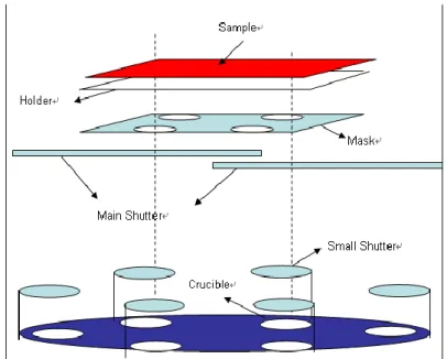
2.4.2 Vacuum thermal evaporation of patterned films
After the routine cleaning procedure, the ITO-coated glasses were loaded on the grounded electrode of a parallel-plate plasma reactor, pretreated by oxygen plasma at 600 W for 20 sec, and then coated with a polymerized fluorocarbon film by trifluoromethane (CHF3) plasma at 100 W for 5 sec, which can improve
the hole injection from ITO anode [8]. Then organic materials were deposited by thermal evaporation at a rate of 0.1 nm/s under the base vacuum of about 10-6 torr in ULVAC SOLCIET coater following a published protocol [9] as illustrated in Figure 2-2. Figure 2-1 also depicts the patterns of organic layers, metal electrode, and active area. In the evaporation of emission layer, the fluorescent dopant was co-deposited with host molecule at its optimal molar ratio. After the thermal deposition of the organic layers and without a vacuum break, 150 nm of aluminum (Al) was deposited through a patterned shadow mask on top of the organic layers using separately controlled sources to complete the cathode. The active area of the OLED device is 9 mm2, which is defined by the overlap of the ITO anode and the metal cathode.
24
Figure 2-2 Schematic diagram of ULVAC SOLCIET coater for thermal deposition of organic materials.
2.4.3 Characterization of device performance
The luminance-current density-voltage (L-J-V) characteristics of the devices were measured with a diode array rapid scan system using Photo Research PR650 spectrophotometer and a DC power supply (Keithley 2400), which are controlled by a computer with a programmable software (Labview v5.1). The color rendering index of white OLED devices were measured by JETI spectroradiometer specbos 1201.
2.4.4 Encapsulation and stability measurement
All devices were sealed prior to testing as illustrated in Figure 2-3. The device lifetime was tested in glove box or in the ambient at a constant drive current density controlled by a DC power supply (Keithley 2400) and the luminance decay was detected by a photodiode connected to data acquisition instruments and a computer with a programmable software (Labview v5.1) as
25 shown in Figure 2-4.
Figure 2-3 Schematic diagram of an encapsulated OLED device.
Figure 2-4 Schematic diagram of device lifetime measurement.
2.5 Charge transport mechanism in disordered organic materials
The transport of charges in disordered organic materials is described as hopping, as they quantum mechanically tunnel to other molecules in the material, sometimes even to nonadjacent ones. This hopping is like a series of redox chemical reactions. The excess electrons and holes are isolated anions and cations, respectively. These ionized species transfer this excess charge to a nearby neutral molecule, thus moving the charge through the material under the
26
influence of the external field even as the molecules themselves remain stationary [10]
To a certain extent theorists borrowed some equations from typical semiconductor theories while tailoring equations to account for the energetic disorder associated arrangement of organic materials. Although there are still some problems for molecular-level simulations, there are a number of characteristics of transport in organic charge transport materials that can be modeled and fit. Usually there are three main dependences of the charge carrier mobility in organics are discussed, they are namely field-dependence, temperature-dependence, and trap-concentration-dependence.
First, the charge mobility in disorder organic materials is known to be dependent on the applied field. The Poole-Frenkel conduction formalism has been shown to be applicable to organic charge transport materials for field dependence within the range of 104 to 106 V/cm [11,12,13], despite some theoretical concerns about its applicability [13]. The Poole-Frenkel dependence of the mobility () is given by the following equation,
) exp( ) (E
0
E
(2.1) where 0 is the zero-field mobility, E is the applied field electric field, and isthe Poole-Frenkel factor.
Secondly, the carrier mobility in these materials depends on temperature. Hopping transport is thermally activated and that means the mobility increases with increasing temperatures, as additional thermal energy is provided to overcome the barriers resulting from energetic disorder. Temperature-dependence in disordered organics can first addresses by formulating a relationship based on the modified Arrhenius equation [14,15]:
27
exp( ) T k T B
(2.2) where ∞ is the mobility at infinite temperature and ∆ is the activation energy.However, as the experimentally accessible temperature ranges are limited for this kind of measurements, other theoretically simulations with different temperature dependence have also been shown to fit well.
The most prominent model for fitting both the field and temperature dependence is Bässler’s disorder formalism [16] as shown below:
2 1/2 2 2 exp 3 2 exp E T k C T k T E, B B σ σ (2.3) where the disorders in both position (including orientational effects) and energy are considered to be Gaussian distributions with widths of Σ and σ , respectively, and C is an empirical constant. The ∞ again represents the infinitetemperature mobility and can be determined by the following equation:
2 0 exp T T T 0 (2.4)The final effect on mobility that must be considered is a compositional change made to the material by altering the concentration of traps within the bulk. Extensive works have been done on molecularly doped polymers and on how the mobility increases with higher content of the active species [17]. Trap-controlled transport has also been studied, with higher concentrations and energetically deeper traps in another transport material causing greater reductions in mobility [18,19,20], as carriers are trapper more frequently and for longer amounts of time before being released (if released at all). The
28
Hoesterey-Letson formalism [21] is a well-known and classic equation to describe the effects on the mobility of a material with a certain relative concentration of traps, as shown below:
T k c c c B t 0 exp 1 1 0 (2.5)in which c is represents the concentration of dopant, (c0) is the trap-free
mobility, and t is the trap energy below the energy level (HOMO or LUMO as
relevant) of majority material.
However, there is a transition to trap-to-trap transport as the concentration of traps rises, where some charge carriers will flow primarily in hops between traps and through the material. This is the case in many mixed transport materials, with two or more charge transport compounds in nearly equal proportions. The transport in such systems is infrequently studied, but a recent theoretical treatment has covered such cases in detail with an extension of the effective medium approximation theory [22].
2.6 TOF measurement
In the field of organic electronics, the measurement of charge carrier mobility is invaluable in understanding how fast a device can respond. Over many years of research, there have been numerous methods developed to test charge transport properties of organic materials with relatively low mobility, such as steady-state space-charge-limited-current (ss-SCLC) [23] and analysis of organic field-effect transistors [24]. Besides, pulsed-radiolysis time-resolved microwave conductivity (PR-TRMC) [25,26] is an indirect method, it only measures the sum of electron and hole mobilities and cannot distinguish which