Effects of Process Temperature on Polysilicon
Thin Film Transistors with Liquid-Phase Deposited
Oxides as Gate Insulators
Ching-Fa Yeh, Tai-Ju Chen,* and Jyh-Nan JengDepartmentof Electronics Engineering and Institute of Electronics, National Chiao-Tung University, Hsinchu 300, Taiwan
ABSTRACT
Liquid-phase deposited (LPD) oxide has previously been successfully applied to low temperature processed polysil-icon thin film transistors (poly-Si TFTs) as a gate insulator. This paper shows the feasibility of applying room tempera-ture deposited LPD oxide to high temperatempera-ture processed devices. The thermal effects of high temperatempera-ture processing on poly-Si TFTs including postoxide annealing and dopant activation have been investigated. These high temperature treat-ments show excellent improvement in device characteristics. In addition, the novel devices also show considerably more efficient hydrogenation during NH3-plasma treatment, and their reliability under dc electrical stress appears similar to that of conventional poly-Si TFTs.
Infroduction
To
develop active matrix liquid crystal displays
(AMLCDs), polysilicon thin film transistors (poly-Si TFTs) in peripheral device circuits must be fabricated either on quartz or on large area glass substrates.1 In addition, in the application of three-dimensional integrated circuits, par-ticularly to static random access memories (SRAM5), poly-Si TFTs are stacked on the top of active elements.2 To date, several gate insulator growth methods have been devel-oped to obtain high performance poly-Si TFTs using either high temperature or low temperature processes.36 Re-cently, great interest has been shown in liquid phase deposited (LPD) oxide films because of their excellent film properties and successful application as gate insulators to low temperature processed (LTP) poly-Si TFTs.6In the application of high temperature-processed (HTP) poly-Si TFTs to SRAMs and quartz based LCDs, thermal oxidation is one of key technologies and can grow high quality gate oxides to bring excellent device characteris-tics. However, thermal oxidation at high temperature (>850°C) has been found to degrade the mobility of poly-Si TFTs.91 The low temperature deposited oxide is an alter-native method for forming gate insulator. Various chemi-cal vapor deposition (CVD) methods have been used to fabricate the gate oxide.3'4 But all of these CVD methods require expensive equipment and the processes involved are very complex. Therefore, we have developed the LPD method to fabricate gate oxide at room temperature. The LPD apparatus used is simple and inexpensive.6-1 LPD oxide technology is thus an economical candidate for replacing high cost CVD technologies. To assess the feasi-bility of applying LPD oxide to HTP poly-Si TFTs, the thermal effects of high temperature processing on TFT performance have to be clarified. In this paper, we focus on the thermal effects of gate oxide annealing and dopant activation of poly-Si TFTs with LPD oxide gate insulators.
In addition, in the poly-Si film there still exists lots of grain boundary defects as well as intragrain defects. It is generally necessary to passivate these defects with
hydro-*ElectrochemicalSociety Student Member.
gen plasma to improve poly-Si TFT performance.'2'13 In this paper, investigation into the effects of NH3-plasma passivation6 on high temperature treated poly-Si TFTs is reported. Moreover, the stability of the novel poly-Si TFTs is of significant importance from the standpoint of long-term operation, so the effects of dc electrical stress on TFT performance are also clarified.
Experimental
The four groups of conventional top gate N-channel poly-Si TFTs shown in Table I were prepared at different temperatures for gate oxide annealing and dopant activa-tion. They are labeled group L-L, group H-L, group L-H, and control. L-L means low gate oxide annealing temper-ature (600°C) and low dopant activation tempertemper-ature (600°C). H—L means high gate oxide annealing temperature (900°C) and low dopant activation temperature (600°C). L-H means low gate oxide annealing temperature (600°C) and high dopant activation temperature (900°C). Group L-L was the conventional LTP poly-Si TFT. Group H-L evaluated the thermal effects of gate oxide annealing on TFTs, while group L-H evaluated the thermal effects of dopant activation. The control sample was the conven-tional HTP poly-Si TFT. The inset in Fig. 1 shows the cross-sectional structure of poly-Si TFTs.
Group L-L, group H-L, and group L-H were prepared according to the following procedures. A 100 nm thick LPCVD amorphous Si layer was deposited on thermal oxide using SiH4 gas at 550°C, and recrystallized at 600°C for 24 h using the solid-phase crystallization (SPC) meth-od. After the SPC poly-Si layer was patterned to the active region, a 47 nm thick gate oxide layer was grown on the active layer using the LPD method at 18°C. 14 For groups L-L and L-H, gate oxide annealing was performed at 600°C for 1 h in N2 ambient. For groups H-L, gate oxide annealing was performed at 900°C for 1 h in N2 ambient. Then, the 300 nm thick poly-Si gates were deposited using the LPCVD method at 620°C. After the poly-Si gates were patterned, the source/drain and gate regions were doped using phosphorus self-aligned ion implantation with an energy of 40 keV and a dose of 5 x 1015 cm2. The LPD oxide upon source/drain regions was not removed, and Table I. Processing conditions for four TFT samples labeled groups [-I, H-I, I-H, and control.
Samples Group L-L Group H-L Group L-H Control Gate insulator LPD oxide ((18°C) LPD oxide (18°C) LPD oxide (18°C) Dry 0 (900°C) Gate-oxide annealing 600°C, 1 h (L) 900°C, 1 h (H) 600°C, 1 h (L) None Dopant activation 600°C, 24 h (L) 600°C, 24 h (L) 900°C, 30 mm (H) 900°C, 30 mm (H)
J. Electrochem. Soc., Vol. 144, No. 10, October 1997 The Electrochemical Society, Inc. 3645 NH5-Plasma treatment
300°C,
3646 J. frlectrocflem. SOC., vol. 144, No. 10, October 1997 ( The Electrochemical Society, Inc. -4 ,—'
w
'S., () I'.) — in-6— lu
io-7L) 108
.
io-9 -5Gate Voltage Vgs (V)
Fig. 1.Transfer characteristics (Id, — Vg,) of poly-Si TFTs (W/L =
20 p.m/5 p.m) at V,,, = 5 V for groups I-I and H-I without hydro-genation. The inset shows the cross-sectional structure of poly-Si
TFTs.
then acts as the screen oxide for ion implantation. For groups L-L and H-L, dopant activation was performed at 600°C for 24 h in N2 ambient. For group L-H, dopant acti-vation was performed at 900°C for 30 mm in N2 ambient. Then, the 500 nm thick oxide interlayer was formed using the PECVD method at 300°C. After the contact holes were opened, 500 nm thick aluminum electrodes were deposited and patterned. Finally, sintering was performed at 400°C for 30 mm in N, ambient.
For the control poly-Si TF'Ts, 47 nm thick gate oxides were prepared using dry oxidation at 900°C without post-oxidation annealing, while dopant activation was per-formed at 900°C for 30 mm in N2 ambient. Other proce-dures are the same as those of group L-L, group H-L, and group L-H.
To passivate the trap states in the poly-Si channel, NH3-plasma hydrogenation was performed for all four groups in a parallel plate reactor at 3 00°C with a power density of 0.7 W/cm2.
Resultsand Discussion
Effectsof processing tern perature.—Figure 1 shows the typical transfer characteristics at V,,,, =5V for groups L-L
and H-L without NH3-plasma treatment. The detailed key device characteristic parameters including threshold volt-age (V,6), subthreshold swing (S.S.), field-effect mobility
(),
and ON/OFF current ratio (I,,,,/4,,,) are shown and analyzed in Table II. We can see that the characteristics of TFTs with high temperature annealed gate oxides (group H-L) are superior to those of conventional LTP devices (group L-L). These improved characteristics, especially their V,,, and S.S., can be attributed to restructuring in the LPD gate oxide and reduction in trap states in the poly-Si film due to postoxide high temperature annealing.As previously reported,'5 essential Si-OH and Si-F bonds exist in as-deposited LPD oxides and greatly affect oxide properties and device characteristics. In the case of gate oxide annealing at 600°C, SiO-H bonds can break,
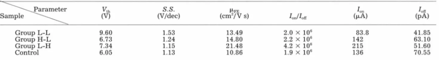
forming large numbers of negatively charged SiO These charges may be the main cause of the high V,6 in group L-L. While annealing at 900°C, in addition to SiO gener-ation, the Si-F bonds even break. The resulting positive Si charges will electrically neutralize many of the nega-tively charged SiO; this is shown by the low V,6 in group H-L. A decrease in Si-F bonds in LPD oxide film during high temperature annealing was observed in FI'IR spectra. Figure 2 shows typical FIR spectra in the region of 700 — 1500
cm' for the as-deposited and the annealed LPD
oxides. In samples annealed at 900°C, the Si-F stretching vibration band (located at 930 cm') has completely disap-peared, and the annealed LPD oxide has come to resemble thermal oxide.'5 Changes in oxide charges due toanneal-ing were also confirmed by the flatband voltage (VFB) shifts in MOS capacitors made from them. MOS capacitors with aluminum gates are not sintered. MOS capacitors 20 made from LPD oxide annealed at 600°C show a VFB of—0.19 V, while those made from LPD oxide annealed at 900°C show a VFB of —1.05 V. The significant negative shift in V implies that lots of positive charges are generated in LPD oxides due to annealing at 900°C.
In addition, the difference in S.S. between group L-L and group H-L is also correlative with fluorine (F) con-centrations in LPD oxides. After 900°C annealing, the diminution in F concentrations causes increases in the dielectric constant of LPD oxide and resultantly in the capacitance.'6'7 This is also a reason for the lower S.S. in group H-L samples.'8
As shown above, high temperature postoxide annealing is effective in enhancing the quality of LPD oxide and in improving the characteristics of poly-Si TFTs. However, in fabricating HTP poly-Si TFrs, dopant activation also needs high temperature annealing. Whether the high tem-perature annealing for dopant activation can availably replace postoxide annealing to improve oxide quality is an interesting issue. We next discuss the effects of annealing for dopant activation on TFT performance.
Figure 3 shows a comparison of typical transfer charac-teristics at Vd. = 5 V for groups H-L, L-H, and control
samples without NH3-plasma treatment. The key device characteristic parameters are also presented and analyzed in Table II. As shown in Fig. 3 and in Table II, group L-H samples showed excellent characteristics including a low V,,, of 7.34 V, a low S.S. of 1.15 V/dec, a high PFE of 21.48 cm2/V s and a high ON-current (I,) of 215 A. The increases in P.FE and I,,, can be attributed to the decrease in drain/source sheet resistance,'9'2° which was 238 f1/E, but 478 hID for group H-L samples. Distinguishing features can be seen more clearly in the output characteristics (I,, — Vth). Figure 4 shows the typical output characteristics
(I, — V,,)of poly-Si TFTs for groups H-L and L-H with V6, as a parameter. High temperature dopant activation in-deed achieves a lower sheet resistance and overwhelming-ly enhances the on-state performance. In addition, com-pared with group L-L, group L-H also exhibits a lower V,6. This indicates that high temperature annealing for dopant activation can also restructure the LPD gate oxide. In total, for group L-H the high temperature treatment effec-tively acts not only as a dopant activator, but also as a gate oxide annealant.
In comparison with the control HTP TFTs, all perfor-mance indexes for group L-H appear favorable; especially the P'FE of 21.48 cm2/V s is excellent. It appears that TF'Ts with LPD gate oxides can have perfect SiO2/poly-Si
inter-Table II. Device characteristic parameters before hydrogenation for groups I-I, H-I, I-H, and control.
0 5 10 15
Vth
(V)
S.S.
(V/dec) (cm2/V s)PFE 'on/loS (p.A)1=
'off (pA) Group L-L Group H-L Group L-H Control 9.60 6.73 7.34 6.05 1.53 1.24 1.15 1.13 13.49 14.80 21.48 10.86 2.0 X 2.2 X 4.2 x 1.9 x 106 106 106 106 83.8 142 215 136 41.85 63.10 51.60 70.55
J. Electrochem. Soc., Vol. 144, No. 10, October 1997 The Electrechemical Seciety, Inc. 3647 (/D
•1
0
CtI
1500 1300 iiOO 900 0 5 10 15Drain Voltage Vds (V)
Wavenumber (cm-1)
700Fig. 2. Changes in FuR spectra in the range of 700 — 1500 cm
for as-deposited and annealed LPD oxides.
faces, while the control TFTs are quite prone to serious roughness problems at Si02/poly-Si interfaces owing to thermal oxidation.9-1'
From the above comparisons among all samples, it can be concluded that as long as high temperature annealing for dopant activation is performed for poly-Si TFTs with LPD gate oxides, more satisfactory device characteristics can be achieved as compared to those exhibited by con-ventional HTP TFTs with thermal gate oxides.
250
a 200
z
t
j
150100
C50
0 20Fig.4. Output characteristics ('d, — VdJ of poly-Si TFTs (W/L = 20pm/S ILm) with Vs,, as a parameter for groups H-I and I-H with-out hydrogenation.
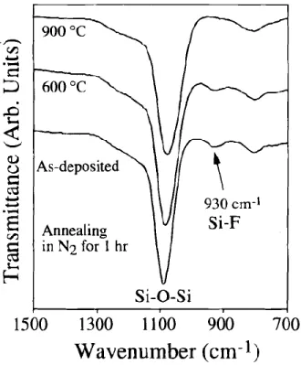
showthe variations in V,handFLFE with NH3-plasma treat-ment time, respectively, for groups L-L, H-L, L-H, and control. For group L-L, the improvement in V,h and PFE wasslight compared with that of the other groups. It has been reported that V,h is mainly influenced by dangling bond midgap states, while IFE is influenced by band tail states in poly-Si TFTs.2' In other words, in high tempera-ture treated devices, the two kinds of trap states are effi-ciently passivated by NH3-plasma treatment. The varia-tions in trap state density (N,) with NH,-plasma treatment time for four groups are shown in Fig. 8. The trap state density (N,) existed in the poly-Si channel is calculated by extracting a straight line on the plot of ln [I/(Vg, —
vs. l/(Vgs — VFB)2at low VdS and high Vgs based on the
fol-lowing equation22
'ds =
(J COXV1FEVgS exp
8CkTCoxVgs
[11
where C0,. is the gate oxide capacitance, q is the electron charge, k is Boltzmann's constant, €s,isthe silicon dielec-tric constant, and T is the temperature. L0 is the channel thickness23
io
i-4
S—, r15t
l0'
V 5U 10
,J I-10-10 1011 Effects of NH3-plasma treetment.—Figure 5 shows thetypical transfer characteristics of groups L-L and L-H at VdS = 5 V before and after 5 h plasma treatment. NH,-plasma treatment improved the performance of both groups. However the improvement in group L-H is more evident. To further investigate the effects of NH,-plasma passivation, the device characteristics were evaluated as a function of NH,-plasma treatment time. Figures 6 and 7
b-3
I
Fig. 3. Transfer characteristics (Id, — V,) of poly-Si TFTs (WilL =
20 pm/S pm), at V, = 5 V for groups 4-i, I-H, and control
with-out hydrogenation.
-7
5 10 Is
Gate
Voltage Vgs (V)
Gate 10 15Voltage Vgs (V)
Fig. 5. Transfer characteristics (Id, — V9J of poly-Si TFTs (WIlL = 20
psm/5 pm) at Vd, = 5 V for groups I-I and I-H before and after S h
3648 J Electrochem. Soc., Vol. 144, No. 10, October 1997 The Electrochemical Society, Inc.
Fig. 6. Variations in threshold voltage with NH3-plasmo
passiva-tion time for groups I-I, H-I, I-H, and control (W/L = 20 pmf5 gm).
8kTt
L =
'V€siOq(17s — VFB)
where t0,, is the gate oxide thickness, €2isthe dielectric constant of gate oxide, and VFB is the gate voltage at which minimum leakage current occurs. For groups H-L, L-H, and control, the N reduction rate caused by NH3 plasma was considerable, while that in group L-L was slight. This is consistent with the results shown in Fig. 6 and Fig. 7, and indicates that the passivation rates for both tail trap states and midgap trap states were significantly increased for high temperature treated poly-Si TFTs.
In our previous report, the shrinkage of LPD oxide after 300, 600, 900, and 1000°C annealing for 1 h in N3 is about 0.07, 1.58, 2.43, and 3.22%, respectively.2425 The quality of LPD oxide after 1000°C annealing is nearly the same as that of thermal oxide, and nearly unchanged under the subsequent annealing. Hence, the differences of LPD gate oxide thickness between LTP and HTP TFTs are small. We can also find that the change from thickness of LPD gate oxide has a small influence on mobility in the comparison
Fig. 8. Variations in trap-state density with NH3-plasma
passiva-tion time for groups I-I, H-I, I-H, and control (W/L =
20 m/5 pm).
between group L-L and group H-L as shown in Table II. Therefore, for high temperature treated TFTs, the fast
[21 changes in mobility during hydrogenation are not due tothe changes in LPD oxide thickness. In addition, the gate
oxides of the control TFTs are different from those of group H-L and L-H. However, group H-L, group L-H, and control TFTs exhibit the same hydrogenation efficiency We can neglect the influence of LPD gate oxide on
mobil-ity during NH3-plasma treatment.
In general, the effects of thermal annealing on poly-Si TFT characteristics are densification in gate oxide, reduc-tion in N of poly-Si channel, and efficient dopant activa-tion. Drain/source sheet resistance does not correlate with the hydrogenation efficiency,26 which can be found in the comparison between group H-L and group L-H. Densifi-cation in gate oxide will reduce the defects in oxide, which may slow the hydrogen diffusion. Hence, we believe that the higher hydrogenation efficiency is related to the reduc-tion in N7 of poly-Si channel for high temperature treated TFTs. It has been reported that midgap states have a faster response to hydrogenation, while tail states respond slow-er to hydrogenation. Only when the hydrogenation con-centration is so large as to fill both the midgap states and the tail states will a significant fraction of the tail states be passivated. Moreover, if the intertor of grains contains a large number of tail states, the passivation rate will be slow for this type of defects.27 For high temperature treat-ed TFTs in this research, both densities of the midgap states and the tail states were reduced by the high temper-ature annealing. Since the density of midgap states was lowered by annealing, this type of defects can be fast filled at the beginning of hydrogenation. Hence, other excess hydrogen atoms can then fast passivate the tail states. The tail states can also have a fast response to hydrogenation. Therefore, at the same hydrogenation condition, both the midgap states and the tail states can be passivated faster then those in group L-L.
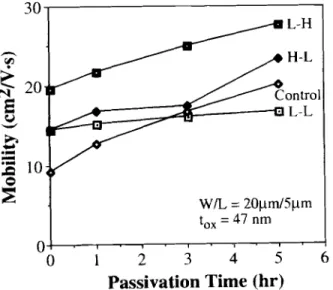
Reliabitity.—The reliability of high temperature treated poly-Si TFTs with LPD oxide gate insulators was investi-gated under dc electrical stress. Figure 9 shows the changes in Vth and S.S. for group L-H as a function of stress time during ON-state stressing with 174, = 17ds = 15V. Both the changes in tVth and ASS. are defined as A(%)=(after stress-before stress)/(bef ore stress) x 100%. Devices with W/L = 5/5 sm had been treated in NH3 plasma for 7 h
before stressing. Both 177h and 5.5. increased with stress time. However, the changes in PFEandminimum OFF-cur-rent after stressing were slight. The stress results for the forward and reverse modes are nearly the same. Hence, the 10 8
6
4
r16
Et. 14
I-C
x12
ct 10 Ga St St2
0
12
34
5 6Passivation
Time (hr)
Passivation Time (hr)
0
1 23
4
5 6Passivation
Time (hr)
Fig- 7. Variations in field-effect mobility with NH3-plasma
passi-vation time for groups I-I, H-L, L-H, and contral (W/L = 20 tm/5 pm)
J. Electrochem. Soc., Vol. 144, No. 10, October 1997 The Electrochemical Society, Inc. 3649
Fig. 9. Degradation rates of threshold voltage (Vth) and sub-threshold swing (S.S.) for group 1-H as a function of stress time under the stress with V,, = = 15 V (W/L = 5/5 .sm).
degradation in group L-H is accounted for by the increase in midgap defects within the poly-Si channel caused by channel carriers.28 Since the LPD oxide was restructured by high temperature annealing and came to resemble ther-mal oxide, interface and bulk dielectric charge-trapping were not the dominant degradation mechanisms as they are in conventional HTP poly-Si TVrs.28
Conclusions
The thermal effects of high temperature processing, including postoxide annealing and dopant activation, on poly-Si TFTh with LPD gate insulators were investigated. The characteristics of TFTs with 900°C annealed LPD gate oxides were superior to those of conventional LTP devices because of densification in the LPD gate oxide and reduc-tion in trap state density. Poly-Si TFTs with only a high temperature dopant activation processing even exhibited more excellent characteristics than conventional HTP poly-Si TFTs with thermal gate oxides due to their perfect Si02/poly-Si interfaces, as well as their restructured LPD gate oxides and efficient dopant activation. For these high
temperature treated devices, both the dangling bond
midgap states and the band tail trap states were more effi-ciently passivated during NH3-plasma treatment. The instability mechanism of high temperature treated TFTs with LPD gate oxides is accounted for by the generation of carrier induced midgap states within the channel. In con-clusion, it has been shown feasible to apply the novel LPD gate oxides as gate insulators to }ITP poly-Si TFTs.Acknowledgment
This
study was supported by the National Science
Council, Republic of China, under Contract No. NSC 85-2215-E-009-036.
Manuscript submitted Jan. 27, 1997; revised manuscript received June 3, 1997.
National Chiao-Tung University assisted in meeting the publication costs of this article.
REFERENCES
1. A. G. Lewis, I.-W. Wu, T. Y. Huang, A. Chiang, and R. H. Bruce, Tech. Dig. mt. Electron Devices Meet., p. 843 (1990).
2. S. D. S. Maihi, H. Shichijo, S. K. Banerjee, R. Sun-daresan, M. Elehy, G. P. Pollack, W. F. Richardson, A. H. Shah, L. R. Hite, R. H. Womack, P. K.
Chat-terjee, and H. W. Lam, IEEE Trans. Electron
Devices, ED-32, 258 (1985).3. Y. S. Kim, K. Y. Choi, and M. K Han, Jpn. J. Appl. Phys., 34, 719 (1995).
4. T. Serikawa, S. Shirai, A. Okamoto, and S. Suyama, IEEE Trans. Electron Devices, ED-36, 1929 (1989). 5. F. S. Wang, M. J. Tsai, and H. C. Cheng, IEEE Electron
Device Lett., ED-16, 503 (1995).
6. C. F Yeh, S. S. Lin, T. Z. Yang, C. L. Chen, and Y. C. Yang, IEEE Trans. Electron Devices, ED-41, 173 (1994).
7. C. F Yeh, S. S. Lin, and C. L. Fan, IEEE Electron De-vice Lett., EDL-16, 473 (1995).
8. C. F Yeh, T. Z. Yang, and T. J. Chen, IEEE Trans. Elec-tron Devices, ED-42, 307 (1995).
9. M. K. Hatalis, J.-H. Kung, J. Kanicki, and A. A.
Bright, MRS Proc. 182, 375 (1990).10. D. N. Kouvatsos, and M. K. Hatalis, IEEE Trans. Elec-tron Devices, ED-43, 1448 (1996),
11. C. A. Dimitriadis, and P. A. Coxon, Appl. Phys. Lett., 54, 620 (1989).
12. T. I. Kamins, and P. J. Marcoux, IEEE Electron Device Lett., EDL-1, 159 (1980).
13. A. Mimura, K. Miyata, T. Suzuki, Y. Hosokawa, H. Kawakami, N. Konishi, Y. A. Ono, K. Ono, and J. Ohwada, IEEE Trans. Electron Devices, ED-36, 351 (1989).
14. C. F Yeh, S. S. Lin, C. L. Chen, and Y. C. Yang, ibid, ED-14,403 (1993).
15. C. F. Yeh, and C. L. Chen, This Journal, 142, 3579 (1995).
16. C. F. Yeh, S. S. Lin, and Water Lu, in 1996 IEEE VLSI Multilevel Interconnection Conference, p. 101, IEEE, Piscatawa, NJ (1996).
17. T. Homma, R. Yamaguchi, and Y. Murao, This Journal,
140,687(1993).
18. 5. M. Sze, Physics of Semiconductor Devices, p. 447, Wiley, New York (1981).
19. M. Matsuo, T. Nakazawa, and H. Ohshima, Jpn. J. Appi. Phys., 31, 4567 (1992).
20. L. Pichon, F Raoult, 0. Bonnaud, J. Pinel, and M. Sarret, IEEE Electron Device Lett., EDL-16, 376 (1995).
21. I-W. Wu, T.-Y. Huang, W. B. Jackson, A. G. Lewis, and A. Chiang, ibid., EDL-12, 181 (1991).
22. J. Levinson, F R. Shepherd, P J. Scanlon, W. D. West-wood, G. Este, and M. Rider, J. Appl. Phys., 53, 1193
(1982).
23. R. E. Proano, R. S. Misage, and D. G. Ast, IEEE Trans. Electron Devices, ED-36, 1915 (1989).
24. C. F Yeh, C. L. Chen, W. Lur, and P W. Yen, Appl. Phys. Lett., 66, 938 (1995).
25. C. L. Chen, Ph.D. Thesis, National Chiao-Tung Uni-versity, Taiwan, (1995).
26. I-W. Wu, A. G. Lewis, T.-Y. Huang, and A. Chiang, IEEE Electron Device Lett., EDL-10, 123 (1989). 27. I-W. Wu, W B. Jackson, T.-Y. Huang, A. G. Lewis, and
A. Chiang, ibid., EDL-11, 167 (1990).
Group L-H Stressed at Vgs =Vds ISV WIL= 5l1m/5tm 5.5 5.0 4.5 4.0