Enhancement of Charge-Storage Performance in Ni-Silicide
Nanocrystal Devices by Thermal Annealing a Ni–Si–N
Thin Film
Wei-Ren Chen,aTing-Chang Chang,b,
*
,zJui-Lung Yeh,a and Chun-Yen Changa aInstitute of Electronics, National Chiao Tung University, Hsin-Chu 300, Taiwan b
Department of Physics and Institute of Electro-Optical Engineering, Center for Nanoscience and Nanotechnology, National Sun Yat-set University, Kaohsiung 804, Taiwan
The stored charge characteristics of Ni-silicide nanocrystals embedded in nitride formed by annealing a Ni–Si–N thin film were studied in this paper. We used X–ray photoelectron spectroscopy, leakage current density, and X-ray diffraction to offer chemical material analysis of nanocrystals with surrounding dielectric and the crystallization of nanocrystals for different thermal annealing treatments. Transmission electron microscope analyses revealed nanocrystals embedded in the nitride layer. Nonvolatile Ni–Si nanocrystal memories with 600°C annealing revealed superior electrical characteristics for charge-storage capacity and reliability compared with the memories with 300 and 500°C annealing. In addition, we used energy-band diagrams to explain the signifi-cance of surrounding dielectric for reliability.
© 2008 The Electrochemical Society. 关DOI: 10.1149/1.2971189兴 All rights reserved.
Manuscript submitted May 27, 2008; revised manuscript received July 18, 2008. Published September 9, 2008.
In recent years, portable electronic products, such as digital cam-eras, notebook computers, MP3 walkmans, intelligent IC cards, USB flash storage disks, etc., have been widely applied daily and play important roles in the consumer market. These electronic prod-ucts are all embedded with flash memory devices. As the demand for flash memory devices grow increasingly, the device density and op-eration speed of flash memory as well as device reliability have also received much attention.1-4 For the development of a next-generation nonvolatile memory共NVM兲 technique, devices should be compatible with the current integrated circuit manufacture process. Therefore, the silicon-oxide-nitride-oxide-semiconductor 共SONOS兲 type and nanocrystals共NCs兲 memory structures have been proposed and demonstrated to lead to an improvement in reliability compared with conventional NVM because of employing discrete traps served as charge-storage media.5,6
In order to overcome the limitations of conventional NVM for the scaling-down process, we proposed memory structures that were combined with SONOS-type and metal NCs to obtain good charge-storage ability and strong coupling with conduction channel. In our work, we used a Ni–Si–N thin film to control the size and distribu-tion of NCs by the internal competidistribu-tion mechanism7and studied the stored charge characteristics of Ni-silicide NCs embedded in nitride under different temperature effects. It was found that the crystalli-zation of NCs and the quality of surrounding dielectric were distinct from the different temperature annealing; and thus that the annealing temperature was a key parameter for the charge-storage properties of NVMs.
Experimental
This memory cell was fabricated on a 4 in. p-type silicon共100兲 wafer with a resistivity of 10⍀ cm. After a standard clean process and native oxide removing, a 5 nm thick tunnel oxide was thermally grown by a dry oxidation process in an atmospheric-pressure chemi-cal vapor deposition furnace. Afterward, a 10 nm thick nitrogen-incorporated Ni0.3Si0.7layer serving as the charge-trapping layer was
deposited by sputtering a Ni0.3Si0.7 commixed target in Ar/N2 共24/10 sccm denotes cubic centimeter per minute at standard tem-perature and pressure兲 environment at room temperature, and the dc sputtering power was set to 80 W 共deposition pressure ⬃7.6 mTorr兲. Here, we could obtain a Ni–Si–N thin layer by X-ray photoelectron spectroscopy 共XPS兲 analysis 共not shown兲. Then, a 30 nm thick blocking oxide was deposited by plasma-enhanced chemical vapor deposition at 300°C. In this study, before blocking
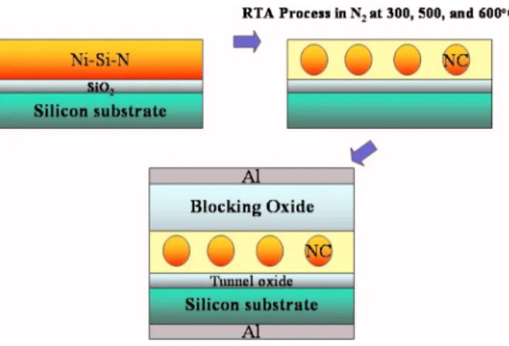
oxide deposition, the charge-trapping layer was annealed at 300°C 共sample A兲, 500°C 共sample B兲, and 600°C 共sample C兲 for 100 s using a rapid thermal annealing system to improve the shape and crystallization of NCs. Finally, Al gate electrodes on the back and front sides of the sample were deposited and patterned to form a metal/oxide/insulator/oxide/silicon共MOIOS兲 structure. The forma-tion flow of the memory cell structure is shown in Fig. 1. Electrical characteristics, including the capacitance–voltage共C-V兲 hysteresis, retention, and endurance characteristics were also performed. The
C-V characteristics were measured by an HP4284 Precision LCR
meter with a high frequency of 1 MHz. In addition, transmission electron microscopy 共TEM兲, XPS, and X-ray diffraction 共XRD兲 were adopted for the microstructure analysis, chemical material analysis, and crystallization of NCs.
Results and Discussion
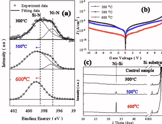
Figure 2 exhibits the material analyses of the charge-trapping layer under the annealing temperature conditions of 300, 500, and 600°C. Figure 2a shows the N 1s core-level spectra with different temperature annealing. Obviously, the spectra are composed of two peaks, SiN共396.8 eV兲 and Ni–N 共398.5 eV兲, for 300 and 500°C annealing.8,9The peak signal of Si–N bonding shifted toward higher binding energy, and the peak signal of Ni–N gradually decayed until it disappeared as the temperature increased. To further ascertain the crystallizations of NCs with different temperature annealing, XRD analyses were executed. As shown in Fig. 2c, the diffraction peak of
*Electrochemical Society Active Member.
z
E-mail: [email protected]
Figure 1. 共Color online兲 Formation flow of the MOIOS structure under
different annealing temperatures共300, 500, and 600°C兲. Journal of The Electrochemical Society, 155共11兲 H869-H872 共2008兲
0013-4651/2008/155共11兲/H869/4/$23.00 © The Electrochemical Society H869
) unless CC License in place (see abstract). ecsdl.org/site/terms_use
address. Redistribution subject to ECS terms of use (see 140.113.38.11
32.8° indicates the Ni–Si NCs are formed with an annealing tem-perature over 500°C.10共The control sample is only a structure of Si substrate with tunnel oxide.兲 From XPS analyses, we considered that the quality of the surrounding dielectric, SiNx, had been improved by a reducible reaction of Ni–N during the thermal annealing pro-cess. To verify this view point, the leakage current density J 共A/cm2兲 with gate voltage was measured 共as shown in Fig. 2b兲. It
was found that the leakage current after 600°C annealing was the lowest under 0 to ⫾10 V sweeping. Moreover, the compound of NCs could be changed from Ni–N to Ni–Si after the annealing pro-cess and also affect charge-storage characteristics for the NVM ap-plication.
In general, the forward 共from accumulation state to inversion state兲 and reverse C-V hysteresis was measured to investigate the
charge-storage abilities of nonvolatile NC memories. Figure 3 pre-sents the memory effect and TEM image 共inset兲 of Ni–N NCs 共sample A兲, and it is clearly observed that memory windows of 1.5 and 3.5 V can be obtained under⫾10 and ⫾12 V operations, re-spectively. When the annealing temperature increases from 300 to 500°C共sample B兲 and 600°C 共sample C兲, the memory win-dow raises to 5.0 V for sample B and 4.0 V for sample C under ⫾10 V sweeping operation. Moreover, these samples also show that the roundness and isolation of NCs are better than for sample A by TEM analyses, as shown in Fig. 4 and 5. These physical phenomena could be contributed by a thermal-enhanced congregation of Ni at-oms. According to a previous theoretical model about the probability of an electron escaping from the NC back to the channel, the spheri-cal NCs can reduce the Weinberg impact frequency, which is af-Figure 2. 共Color online兲 共a兲 N 1s XPS
analysis of NCs 共empty circles and straight line indicate experimental and fit-ting results, respectively兲. 共b兲 Leakage current density共A/cm2兲 with gate voltage
and共c兲 XRD analysis of NCs during dif-ferent thermal annealing temperatures.
Figure 3. C-V hysteresis and TEM image共inset兲 of nonvolatile Ni–N NC
memories共300°C兲. The memory window was 1.5 V under ⫾10 V opera-tion.
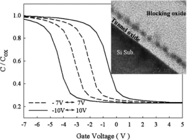
Figure 4. C-V hysteresis and TEM image共inset兲 of nonvolatile Ni–Si NC
memories共500°C兲. The memory window was 5.0 V under ⫾10 V opera-tion.
H870 Journal of The Electrochemical Society, 155共11兲 H869-H872 共2008兲
H870
) unless CC License in place (see abstract). ecsdl.org/site/terms_use
address. Redistribution subject to ECS terms of use (see 140.113.38.11
fected by the geometry effect.11The more-separated NCs could also restrain the electrons’ lateral migration effect under a retention test, because the electrons stored in the NC lift the energy level of the NC conduction band, resulting in the increase of the escaping probabil-ity. Therefore, the rotundity and severance of NCs are good for the sub-50 nm gate-length process application.
We further compared charge-storage characteristics of samples A–C such as the memory window, retention, and endurance. The results are listed in Table I. The memory window of sample B is three times larger than that of sample A. Because the resistivity of Ni–Si NCs 共14–20 ⍀ cm兲 is smaller than Ni–N NCs 共151.7 ⍀ cm兲 and the resistivity is inverse with the density of states, which is a property that affects the number of storage charges,12sample B has a superior memory window due to a lower amount of Ni–N NCs共as shown in Fig. 2兲. Hence, it is believed that the nonvolatile memory capacity was greatly influenced by the crys-tallizations characteristic of Ni–Si and Ni–N NCs. In addition, the initial memory window was fixed at the same value for the retention and endurance test. The memory window of retention was obtained by comparing the C-V curves from a charged state 共write/erase 共W/E兲 state兲 and the quasi-neutral state, for which we used an ex-trapolation共between 1–104s兲 to give a long-term predictable result
共10 years兲. Furthermore, the W/E biases for endurance were set at
VG-Vflatband= ⫾5 V for 0.1 ms 共this condition was enough to define
the data information for the current NVMs兲. Table I clearly indicates that the reliability of nonvolatile Ni–Si NCs memories 共sample B and sample C兲 is better than Ni–N NCs 共sample A兲. According to the
above-mentioned material analyses, we concluded that the annealing temperature had a great influence on the properties of NCs, and this factor also significantly affected the memory window.
Here, the conjectural energy-band diagrams were proposed to explain these physical phenomena of charge storage, as shown in Fig. 6. Because the density of traps in the nitride layer decreased as the annealing temperature increased, sample C 共600°C兲 had the least trap density, as shown in Fig. 6c. However, the reduction in trap density resulted in a memory window in sample C that was Figure 5. C-V hysteresis and TEM image共inset兲 of nonvolatile Ni–Si NC
memories共600°C兲. The memory window was 4.0 V under ⫾10 V opera-tion.
Table I. Comparison table for the memory window retention, and endurance. The initial memory window was fixed at the same value for the retention and endurance test.
Memory window under ⫾10 V Memory window after 10 years 共retention: electrons holding ratio兲 Memory window after 106W/E cycles共endurance兲 Sample A 共300°C兲 1.5 V 0.5 V共20%兲 1.0 V共degradation 50%兲 Sample B 共500°C兲 5.0 V 0.7 V共31%兲 2.1 V共degradation 0%兲 Sample C 共600°C兲 4.0 V 1.1 V共50%兲 2.1 V共degradation 0%兲
Figure 6. Energy-band diagrams of共a兲 Ni–N NCs 共300°C兲, 共b兲 Ni–Si NCs
共500°C兲, and 共c兲 Ni–Si NCs 共600°C兲 embedded in the nitride layer.
H871
Journal of The Electrochemical Society, 155共11兲 H869-H872 共2008兲 H871
) unless CC License in place (see abstract). ecsdl.org/site/terms_use
address. Redistribution subject to ECS terms of use (see 140.113.38.11
lower than that of sample B, because the traps of nitride could provide additional charge-storage nodes. Although the nitride traps can improve the memory window, electrons stored in these shallow traps of nitride easily escape to the substrate. In addition, the nitride traps surrounding the NCs also provide leakage paths for the stored carriers of NCs. Both the above drawbacks cause the retention of samples A and B to be worse than sample C. As shown in Table I, the electron holding ratio of 50% of sample C, estimated for 10 years, is much better than sample B共31%兲 and A 共20%兲. More-over, the endurance results reveal that samples B and C had excel-lent reliability after 106W/E cycles operation, because the stronger silicon–nitrogen bonding共as shown in Fig. 2a兲 could suppress the damage during W/E operation. Summarizing the above results, the nonvolatile Ni–Si NC memory after an annealing temperature of 600°C exhibits the best NVM performance, and this device can also be used on a low-temperature substrate 共⬍600°C兲 for next-generation applications.
Conclusion
In conclusion, the nonvolatile memory characteristics were influ-enced by the crystallizations of Ni–Si and Ni–N NCs. The nonvola-tile Ni–Si NC memory showed better charge storage ability and reliability than nonvolatile Ni–N NCs memory, because Ni–Si NCs have higher density of states and stronger surrounding dielectric than the others. Hence, the MOIOS structure needed a 600°C ther-mal annealing process to obtain a high-performance nonvolatile NC memory in this work. In addition, the proposed energy-band dia-grams could clearly explain the trap density of surrounding dielec-tric, SiNx, and how it affected the NVM characteristics.
Acknowledgments
This work was performed at the National Nano Device Labora-tory 共P-96-1A-062兲 and was supported by the National Science Council of the Republic of China共Taiwan兲 under contract no. NSC 96-2221-E-009-202-MY3, no. NSC 96-2120-M-110-001, no. NSC 95-2221-E-009-296-MY2, and no. NSC 96-2112-M-110-013.
National Sun Yat-Sen University assisted in meeting the publication costs of this article.
References
1. S. Tiwari, F. Rana, K. Chan, H. Hanafi, W. Chan, and D. Buchanan, Tech. Dig. -Int. Electron Devices Meet., 1995, 521.
2. W. R. Chen, T. C. Chang, P. T. Liu, P. S. Lin, C. H. Tu, and C. Y. Chang, Appl. Phys. Lett., 90, 112108共2007兲.
3. J. D. Blauwe, IEEE Trans. Nanotechnol., 1, 72共2002兲.
4. Z. Liu, C. Lee, V. Narayanan, G. Pei, and E. C. Kan, IEEE Trans. Electron Devices,
49, 9共2002兲.
5. C. H. Lee, S. H. Hur, Y. C. Shin, J. H. Choi, D. G. Park, and K. Kim, Appl. Phys. Lett., 86, 152908共2005兲.
6. T. C. Chang, P. T. Liu, S. T. Yan, and S. M. Sze, Electrochem. Solid-State Lett., 8, G71共2005兲.
7. W. R. Chen, T. C. Chang, P. T. Liu, J. L. Yeh, C. H. Tu, J. C. Lou, C. F. Yeh, and C. Y. Chang, Appl. Phys. Lett., 91, 082103共2007兲.
8. I. Crupi, D. Corso, G. Ammendola, S. Lombardo, C. Gerardi, B. DeSalvo, G. Ghibaudo, E. Rimini, and M. Melanotte, IEEE Trans. Nanotechnol., 2, 4共2003兲. 9. Y. Wang, Z. W. Fu, X. L. Yue, and Q. Z. Qin, J. Electrochem. Soc., 151, E162
共2004兲.
10. J. F. Liu, H. B. Chen, J. Y. Feng, and J. Zhu, Appl. Phys. Lett., 77, 2177共2000兲. 11. M. She and T. J. King, IEEE Trans. Electron Devices, 50, 9共2003兲.
12. N. S. Gajbhiye, R. S. Ningthoujam, and J. Weissmuller, Phys. Status Solidi A, 189, 691共2002兲.
H872 Journal of The Electrochemical Society, 155共11兲 H869-H872 共2008兲
H872
) unless CC License in place (see abstract). ecsdl.org/site/terms_use
address. Redistribution subject to ECS terms of use (see 140.113.38.11